# PCI-6202

16-bit High-Resolution

Voltage Output Card

User's Manual

Manual Rev. 2.00

Revision Date: March 17, 2008

Part No: 50-11235-1000

![The image displays a black circular icon containing the white universal recycling symbol. The symbol consists of three arrows arranged in a triangular loop, chasing each other in a clockwise direction. Each arrow is depicted with a stylized, three-dimensional appearance, featuring parallel lines along the right side of the arrow shaft.](.pci-6202-manual-4/cd51e387e2275e877f520510661ec71325650f5af15e8ccbb73d196c78d4afc0.jpg)
Recycled Paper

Copyright 2008 ADLINK TECHNOLOGY INC.

All Rights Reserved.

The information in this document is subject to change without prior notice in order to improve reliability, design, and function and does not represent a commitment on the part of the manufacturer.

In no event will the manufacturer be liable for direct, indirect, special, incidental, or consequential damages arising out of the use or inability to use the product or documentation, even if advised of the possibility of such damages.

This document contains proprietary information protected by copyright. All rights are reserved. No part of this manual may be reproduced by any mechanical, electronic, or other means in any form without prior written permission of the manufacturer.

# Trademarks

NuDAQ, NuIPC, DAQBench are registered trademarks of ADLINK TECHNOLOGY INC.

Product names mentioned herein are used for identification purposes only and may be trademarks and/or registered trademarks of their respective companies.

# Getting service

Customer satisfaction is our top priority. Contact us should you require any service or assistance.

# ADLINK TECHNOLOGY INC.

Web Site http://www.adlinktech.com

Sales & Service service@adlinktech.com

Telephone No. +886-2-8226-5877

Fax No. +886-2-8226-5717

Mailing Address 9F No. 166 Jian Yi Road, Chungho City,

Taipei Hsien 235, Taiwan, ROC

# ADLINK TECHNOLOGY AMERICA, INC.

Sales & Service info@adlinktech.com

Toll-Free +1-866-4-ADLINK (235465)

Fax No. +1-949-727-2099

Mailing Address 8900 Research Drive, Irvine,

CA 92618, USA

# ADLINK TECHNOLOGY EUROPEAN SALES OFFICE

Sales & Service emea@adlinktech.com

Toll-Free +49-211-4955552

Fax No. +49-211-4955557

Mailing Address Nord Carree 3, 40477 Düsseldorf, Germany

# ADLINK TECHNOLOGY SINGAPORE PTE LTD

Sales & Service singapore@adlinktech.com

Telephone No. +65-6844-2261

Fax No. +65-6844-2263

Mailing Address 84 Genting Lane #07-02A,

Cityneon Design Center, Singapore 349584

# ADLINK TECHNOLOGY INDIA LIAISON OFFICE

Sales & Service india@adlinktech.com

Telephone No. +91-80-57605817

Fax No. +91-80-26671806

Mailing Address No. 1357, Ground Floor, "Anupama",

Aurobindo Marg JP Nagar (Ph-1)

Bangalore - 560078

# ADLINK TECHNOLOGY KOREA

Sales & Service korea@adlinktech.com

Telephone No. +82-2-20570565

Fax No. +82-2-20570563

Mailing Address #402, Dongsung B/D, 60-12,

Nonhyeon-Dong Gangnam-gu,

Seoul, 135-010, South Korea

# ADLINK TECHNOLOGY BEIJING

Sales & Service market@adlinkchina.com.cn

Telephone No. +86-10-5885-8666

Fax No. +86-10-5885-8625

Mailing Address Room 801, Building E, Yingchuangdongli

Plaza, No.1 Shangdidonglu,

Haidian District, Beijing, China

# ADLINK TECHNOLOGY SHANGHAI

Sales & Service market@adlinkchina.com.cn

Telephone No. +86-21-6495-5210

Fax No. +86-21-5450-0414

Mailing Address Floor 4, Bldg. 39, Caoheting Science and

Technology Park, No.333 Qinjiang Road,

Shanghai, China

# ADLINK TECHNOLOGY SHENZHEN

Sales & Service market@adlinkchina.com.cn

Telephone No. +86-755-2643-4858

Fax No. +86-755-2664-6353

Mailing Address C Block, 2nd Floor, Building A1,

Cyber-tech Zone, Gaoxin Ave. 7.S,

High-tech Industrial Park S.,

Nanshan District, Shenzhen,

Guangdong Province, China

# Using this manual

# 1.1 Audience and scope

This manual guides you when using ADLINK multi-function data acquisition PCI card. The card's hardware, signal connections, and calibration information are provided for faster application building. This manual is intended for computer programmers and hardware engineers with advanced knowledge of data acquisition and high-level programming.

# 1.2 How this manual is organized

This manual is organized as follows:

Chapter 1 Introduction: This chapter introduces the ADLINK PCI-6202 card including its features, specifications, software support information, and package contents.

Chapter 2 Hardware Information: This chapter presents the card's layout and connector pin definition.

Chapter 3 Installation: This part describes the PCI-6202 installation, and configuration.

Chapter 4 Operation Theory: The operation theory of the PCI-6202 functions including D/A conversion, isolation DIO, and application function I/O are discussed in this chapter.

Chapter 5 Calibration: The chapter offers information on how to calibrate the PCI-6202 for accurate data acquisition and output.

Warranty Policy: This presents the ADLINK Warranty Policy terms and coverages.

# 1.3 Conventions

Take note of the following conventions used throughout the manual to make sure that you perform certain tasks and instructions properly.

NOTE Additional information, aids, and tips that help you perform particular tasks.

IMPORTANT Critical information and instructions that you MUST perform to complete a task.

WARNING Information that prevents physical injury, data loss, module damage, program corruption, and others when trying to complete a particular task.

# Table of Contents

# List of Tables...... iii

# List of Figures ...... iv

# 1 Introduction ...... 1

1.1 Features.... 2
1.2 Applications 2
1.3 Specifications.... 3
1.4 Unpacking Checklist 5
1.5 Software Support 6
Driver Support for Windows 7

# 2 Hardware Information 11

2.1 Card Layout 11
2.2 Connector Pin Assignment 11
CN1 Pin Assignment 12
CN2 Pin Assignment 13
Signal Descriptions 14

# 3 Installation 15

3.1 Before You Proceed 15
3.2 Installing the Card.... 15
3.3 Configuring the Card.... 16
Configuration 16
Troubleshooting 16

# 4 Operation Theory 17

4.1 Block Diagram 17
4.2 D/A Conversion.... 18
Software Update 20
Waveform Generation 21

4.3 General Purpose Digital D/O 28

General Purpose Timer/Counter 31

4.4 Isolation Encoder 38

4.5 Isolated Digital Output 43

4.6 Isolated Digital Input 43

# 4.7 Trigger Sources 44

Software Trigger 44

External Digital Trigger 44

# 5 Calibration 45

# Warranty Policy 47

# List of Tables

Table 2-1: CN1 Pin Assignment 12

Table 2-2: CN2 Pin Assignment 13

Table 2-3: I/O Signal Description 14

Table 4-1: Bipolar Output Codes 20

Table 4-2: Summary of Counters for Waveform Generation ... 21

Table 4-3: TTL DIO Pins in CN1 28

Table 4-4: AFI Functions 29

Table 4-5: Timer/Counter Mode Pins in CN1 31

Table 4-6: Encoder Pins in CN2 38

# List of Figures

Figure 1-1: ADLINK Software Support Overview 6

Figure 1-2: DAQPilot Main Interface 7

Figure 1-3: DAQMaster Device Manager....8

Figure 1-4: Legacy Software Support Overview 9

Figure 2-1: PCI-6202 Layout.... 11

Figure 4-1: PCI-6202 Block Diagram 17

Figure 4-2: Block Diagram of D/A Conversion Function ..... 18

Figure 4-3: FIFO Data In/Out Structure.... 19

Figure 4-4: Waveform Generation for Three Channels Update. 19

Figure 4-5: Typical D/A Timing of Waveform Generation ..... 22

Figure 4-6: Post-Trigger Generation 23

Figure 4-7: Delay-Trigger Generation 24

Figure 4-8: Post-Trigger with Retrigger Generation 25

Figure 4-9: Finite Iterative Waveform Generation with Post-trigger 26

Figure 4-10: Infinite Iterative Waveform Generation with Post-trigger 26

Figure 4-11: PWM Output Parameters.... 30

Figure 4-12: Mode 1 Operation.... 33

Figure 4-13: Mode 2 Operation.... 33

Figure 4-14: Mode 3 Operation.... 34

Figure 4-15: Mode 4 Operation.... 34

Figure 4-16: Mode 5 Operation 35

Figure 4-17: Mode 6 Operation 35

Figure 4-18: Mode 7 Operation 36

Figure 4-19: Mode 8 Operation 36

Figure 4-20: Mode 9 Operation.... 37

Figure 4-21: Mode 10 Operation.... 37

Figure 4-22: Encoder Isolation Input Module 39

Figure 4-23: Encoder OGRx Input 39

Figure 4-24: CW/CCW Encoder Timing 40

Figure 4-25: X1 Encoder Mode 40

Figure 4-26: X2 Encoder Mode 41

Figure 4-27: X4 Encoder Mode 41

Figure 4-28: Phase Z 42

Figure 4-29: Isolated Digital Output 43

Figure 4-30: Isolated Digital Input 43

Figure 4-31: External Digital Trigger 44

# 1 Introduction

The ADLINK PCI-6202 is a 4-channel, 16-bit high-resolution voltage output card with hardware timed waveform generation. It comes with four analog output channels that update simultaneously and support up to 1 MS/s update rate per channel. Delivering excellent linearity (DNL &lt;1 LSB), the PCI-6202 is suitable for dynamic signal simulation and control applications which require high accuracy through voltage output.

The PCI-6202 also provides additional I/O control lines for system integration, including 16-CH isolated digital input and 16-CH isolated output, 8-CH TTL DI and 8-CH TTL DO, 3-CH encoder inputs, and 4-CH PWM outputs. These high-performance I/O functionalities combined with a solid voltage output linearity and high accuracy, make the PCI-6202 the best single-board solution for both equipment manufacturers and laboratory research applications.

# 1.1 Features

The PCI-6202 comes with the following features:

▶ Supports a 32-bit 3.3 V or 5 V PCI bus
▶ PCI 2.3-compliant
▶ 4-CH single-ended analog output
▶ 1 MS/s with simultaneous update
▶ FIFO with 512 samples
▶ 8-CH TTL digital input and 8-CH TTL digital output
▶ 16-CH isolated digital input and 16-CH isolated digital output
▶ 2-CH 32-bit 40 MHz general purpose timer/counters
▶ 3-CH 4 MHz encoder input, supporting AB phase and CW/CCW
▶ 4-CH PWM output
▶ 3-CH digital application function interface with:
▷ Digital input and output
▷ External digital trigger in and out
▷ External analog output conversion clock source
▷ Encoder trigger out

# 1.2 Applications

The PCI-6202 is suitable for the following applications:

▶ Automotive testing
▶ Waveform generation

# 1.3 Specifications

&lt;table&gt;<tr><td colspan="2">Analog Output (AO)</td></tr><tr><td>Number of channels</td><td>4</td></tr><tr><td>D/A converter</td><td>Onboard converter</td></tr><tr><td>Maximum update range</td><td>1 MS/s per channel</td></tr><tr><td>Resolution</td><td>16-bit</td></tr><tr><td>Data transfers</td><td>Programmed I/O, DMA</td></tr><tr><td>Output range</td><td>±10 V</td></tr><tr><td>Settling time</td><td>3 μs (0.1% of full scale)</td></tr><tr><td>Slew range</td><td>20 V/μS</td></tr><tr><td>Rise time</td><td>0.67 V/μS (typical)</td></tr><tr><td>Fall time</td><td>20V/μS</td></tr><tr><td>Maximum DNL</td><td>±1 LSB</td></tr><tr><td>Output coupling</td><td>DC</td></tr><tr><td>Output impedance</td><td>0.01 Ω (maximum)</td></tr><tr><td>Output driving</td><td>±5 mA (maximum)</td></tr><tr><td>Stability</td><td>Any passive load, up to 1500 pF</td></tr><tr><td>Power-on state</td><td>0 V</td></tr><tr><td>Power-on glitch</td><td>6.25 mV/ms (maximum)</td></tr><tr><td>Offset error</td><td>After calibration: ±0.3 mV (typical)</td></tr><tr><td>Gain error</td><td>After calibration: ±0.06 mV (maximum)</td></tr><tr><td colspan="2">Isolated Digital Input</td></tr><tr><td>Number of channels</td><td>16</td></tr><tr><td>Photo isolator</td><td>PC3H410 or equivalent</td></tr><tr><td>Isolation voltage</td><td>2500 Vrms</td></tr><tr><td>Input voltage</td><td>Up to 24 VDC, non-polarity• Logic low: VIL = 0 to 3.0 V• Logic high: VIH = 3.2 V to 2.4 V</td></tr><tr><td>Input resistance</td><td>4.7 KΩ @ 0.12 W</td></tr></table>

Isolated Digital Output

<table><tr><td>Number of channels</td><td>16</td></tr><tr><td>Photo isolator</td><td>PC3H7 or equivalent</td></tr><tr><td>Isolation voltage</td><td>2500 Vrms</td></tr><tr><td>Output type</td><td>Photo-coupler transistors, open collector up to 24 VDC</td></tr><tr><td>Sink current</td><td>200 mA for each channel (maximum)</td></tr></table>

Digital I/O

<table><tr><td>Number of channels</td><td>8-CH TTL digital input8-CH TTL digital output3-CH Application Function Interface (AFI)</td></tr><tr><td>Input voltage</td><td>Logic low:  $VIL = 0.8V$  max;  $IIL = 0.2mA$  maxLogic high:  $VIH = 2.0V$  min;  $IIH = 0.2mA$  max</td></tr><tr><td>Output voltage</td><td>Logic low:  $VOL = 0.5V$  max;  $IOL = 10mA$  maxLogic high:  $VOH = 2.6V$  min;  $IIH = 10mA$  max</td></tr></table>

Timer/Counter

<table><tr><td>Type</td><td>2-CH 32-bit general-purpose timer/counters</td></tr><tr><td>Clock source</td><td>Internal or external</td></tr><tr><td>Maximum source frequency</td><td>• Internal: 80 MHz• External: 10 MHz</td></tr></table>

Encoder Inputs

<table><tr><td>Number of channels</td><td>3</td></tr><tr><td>Maximum input frequency</td><td>4 MHz</td></tr><tr><td>Encoder count</td><td>19-bit data width</td></tr><tr><td>Photo isolator</td><td>Photo isolator</td></tr><tr><td>Encoder modes</td><td>CW/CCWX1 AB phase encoderX2 AB phase encoderX4 AB phase encoder</td></tr></table>

PWM Outputs

<table><tr><td>Number of channels</td><td>4</td></tr><tr><td>Duty cycle</td><td>1 - 99%</td></tr><tr><td>Modulation frequency</td><td>20 MHz to 0.005 Hz</td></tr></table>

Specifications are subject to change without notice.
Isolated 5V Output

<table><tr><td>Driving current</td><td>350 mA (maximum)</td></tr><tr><td colspan="2">Physical, Power, and Operating Environment</td></tr><tr><td>Dimension</td><td>120 mm x 87 mm</td></tr><tr><td>I/O connector</td><td>2 x 68-pin SCSI-VHDCI connectors</td></tr><tr><td>Power Requirement(typical)</td><td>• +5 VDC: 500 mA• +12 VDC: 110 mA</td></tr><tr><td>Operating environment</td><td>• Ambient temperature: 0°C to 45°C• Relative humidity: 10% to 90%,non-condensing</td></tr><tr><td>Storage environment</td><td>• Ambient temperature: -20°C to 80°C• Relative humidity: 5% to 95% non-condensing</td></tr></table>

# 1.4 Unpacking Checklist

Before unpacking, check the shipping carton for any damage. If the shipping carton and/or contents are damaged, inform your dealer immediately. Retain the shipping carton and packing materials for inspection. Obtain authorization from your dealer before returning any product to ADLINK.

Check if the following items are included in the package.

▶ PCI-6202 multi-function DAQ card
▶ ADLINK All-in-One CD
▶ User's manual

If any of the items is damaged or missing, contact your dealer immediately.

# CAUTION

The card must be protected from static discharge and physical shock. Never remove any of the socketed parts except at a static-free workstation. Use the anti-static bag shipped with the product to handle the card. Wear a grounded wrist strap when servicing.

# 1.5 Software Support

ADLINK provides comprehensive software drivers and packages to suit various user approach to building a system. Aside from programming libraries, such as DLLs, for most Windows-based systems, ADLINK also provides drivers for other application environment such as LabVIEW $^{®}$ and MATLAB $^{®}$ . ADLINK also provides ActiveX component ware for measurement and SCADA/HMI, and breakthrough proprietary software applications.

All software options are included in the ADLINK All-in-One CD.

![The diagram presents a layered software and hardware stack for Data Acquisition (DAQ). From top to bottom, the labeled blocks and connections are:\n\n**Top Layer (Application/Development Environment):**\n*   **Label:** ADE\n*   **Block:** VB.NET/C#/NET/VC++/VB/Delphi/BCB etc.\n*   **Block:** LabVIEW\n*   **Block:** MATLAB\n*   **Block:** DAQMaster Configuration based System Manager For ADLINK DAQ Devices\n\n**Second Layer (Library):**\n*   **Label:** Library\n*   **Block:** DAQBench PCIS-/D2K/-WD-OCX ActiveX Control\n*   **Block:** DAQPilot ActiveX Control & .NET Assembly\n*   **Block:** ADLINK DAQ-VIEWPnP VI Library\n*   **Block:** ADLINK DAQ-MTLB DAQ Toolbox\n*   **Connection:** Two blue arrows point downwards from the 'Library' row blocks (specifically below DAQBench and DAQPilot) towards the 'Driver' row.\n\n**Third Layer (Driver):**\n*   **Label:** Driver\n*   **Block:** D2K-/PCIS/-WD-DASK\n*   **Block:** DAQPilot Drivers (Task-oriented)\n\n**Fourth Layer (Operating System):**\n*   **Label:** Operating System\n*   **Block:** Windows 98/NT/2K/XP/Vista x86\n*   **Block:** Windows XP x64/Server 2003 x64/Vista x64\n\n**Bottom Layer (Hardware):**\n*   **Label:** ADLINK DAQ Cards\n*   **Block:** (General-Purpose DAQ, Digital I/O, Analog Output, Performance DAQ, PXI, High-Speed Digital I/O, Digitizer)](.pci-6202-manual-4/f4592820b573aa95ec4bdba6a8f3925b60db8ddb29cf8447685ffaba0fe47dcf.jpg)

Figure 1-1: ADLINK Software Support Overview

# Driver Support for Windows

# DAQPilot

DAQPilot is a driver and SDK with a graphics-driven interface for various application development environments. DAQPilot comes as ADLINK's commitment to provide full support to its comprehensive line of data acquisition products and is designed for the novice to the most experienced programmer.

![DAQPilot\nANALOG INPUT\nANALOG OUTPUT\nDIGITAL INPUT\nDIGITAL OUTPUT\nTIMER/CTR\nYour pilot to\ndata acquisition world\nADLINK\nTECHNOLOGY INC.\nCopyright © 2007 ADLINK Technology Inc. All Rights Reserved.](.pci-6202-manual-4/ceeb4cf4895c31e9759c65a959bcf1cceffbecbadac70137c3ad7a98bdf26c77.jpg)

Figure 1-2: DAQPilot Main Interface

As a task-oriented DAQ driver, SDK and wizard for Windows systems, DAQPilot helps you shorten the development time while accelerating your learning curve for data acquisition programming.

You can download and install DAQPilot at http://www.adlinktech.com/TM/DAQPilot.html

# DAQMaster

The ADLINK DAQMaster is a smart device manager that opens up access to ADLINK data acquisition and test and measurement products. DAQMaster delivers all-in-one configurations and provides you with a full support matrix to properly and conveniently configure ADLINK Test and Measurement products.

![DAQMaster\nDevice Manager\nSoftware Manager\nTask Manager\nProducts\nADLINK Test & Measurement\nDevice Overview Support Matrix\n# Type Model Form Factor Driver ComponentWare\nPCI LPCI sPCI PCIe PS0 Windows Linux MD/Bench ComponentWare\n1 Analog Output Modules 62085216 v v PGS-DASK POS-DASK v POS-OCX\n2 6308 v PGS-DASK POS-DASK v POS-OCX\n3 7200 v PGS-DASK POS-DASK v POS-OCX\n4 7224 v PGS-DASK POS-DASK v POS-OCX\n5 7230 v PGS-DASK POS-DASK v POS-OCX\n6 7233 v PGS-DASK POS-DASK v POS-OCX\n7 7234 v PGS-DASK POS-DASK v POS-OCX\n8 7240 v PGS-DASK POS-DASK v POS-OCX\n9 7243 v PGS-DASK POS-DASK v POS-OCX\n10 7250 v PGS-DASK POS-DASK v POS-OCX\n11 7252 v PGS-DASK POS-DASK v POS-OCX\n12 7256 v PGS-DASK POS-DASK v\n13 Digital IO Modules 7258 v PGS-DASK POS-DASK v\n14 Digital IO Modules 7260 v PGS-DASK POS-DASK v\n15 7266 v PGS-DASK POS-DASK v POS-OCX\n16 7300 v PGS-DASK POS-DASK v POS-OCX\n17 7432 v PGS-DASK POS-DASK v POS-OCX\n18 7433 v PGS-DASK POS-DASK v POS-OCX\n19 7434 v PGS-DASK POS-DASK v POS-OCX\n20 7442 v PGS-DASK POS-DASK v\n21 7443 v PGS-DASK POS-DASK v\n22 7444 v PGS-DASK POS-DASK v\n23 7452 v PGS-DASK POS-DASK v\n24 7348 v PGS-DASK POS-DASK v POS-OCX\n25 7366 v PGS-DASK POS-DASK v POS-OCX\n26 Digitizer Modules 981059012 v PGS-DASK POS-DASK v POS-OCX\n27 Product Support Matrix Tied Party Support & Application\nDevice Manager(Installed) Drag the selected device item to subfunction button to launch\nCalibrates DAQ-2000 series modules](.pci-6202-manual-4/e53dab794064c6d8faaf938b51133c7759771d68fe47d519f8f89068b5f3cdda.jpg)

Figure 1-3: DAQMaster Device Manager

As a configuration-based device manager for ADLINK DAQ cards, DAQMaster enables you to manage ADLINK devices and interfaces, install and upgrade software applications, and manage ADLINK DAQPilot tasks.

# PCIS-DASK (Legacy Drivers and Support)

PCIS-DASK is composed of advanced 32-bit kernel drivers for customized DAQ application development. PCIS-DASK enables you to perform detailed operations and achieve superior performance and reliability from your data acquisition system. DASK kernel drivers now support the revolutionary Windows Vista® OS.

![This diagram illustrates a software architecture stack, divided into 'User Mode' and 'Kernel Mode'.\n\n**Labeled Blocks:**\n\n*   **Top Headers:** 'User Mode', 'Kernel Mode'\n*   **Left Column (User Mode Applications/Languages):**\n    *   'Delphi'\n    *   'BCB'\n    *   'VC++'\n    *   'VB'\n    *   'VB.NET'\n    *   'C#'\n*   **Blue Oval Blocks (User Mode):**\n    *   'PCIS-DASK'\n    *   'D2K-DASK'\n    *   'WD-DASK'\n*   **Kernel Mode Components:**\n    *   Vertical Blue Bar: 'System Service'\n    *   Grid Blocks:\n        *   'Process Structure'\n        *   'Object Manager'\n        *   'Memory Manager'\n        *   'Configuration Manager'\n        *   'I/O Manager'\n        *   'DASK Kernel Driver (.sys)' (Red text)\n        *   'Executive Support'\n        *   'Plug and Pay'\n        *   'Power Manager'\n        *   'File System'\n        *   'Lowest-level Driver'\n    *   Vertical Blue Bars (Right side):\n        *   'Hardware Abstraction Layer'\n        *   'Hardware'\n\n**Connections:**\n\n*   **Orange Arrows (User to Kernel):** Single-headed arrows pointing from the blue ovals ('PCIS-DASK', 'D2K-DASK', 'WD-DASK') to the 'System Service' bar.\n*   **Orange Arrows (Kernel to Hardware):**\n    *   A single-headed arrow pointing from 'Lowest-level Driver' to the 'Hardware Abstraction Layer'.\n    *   A double-headed arrow connecting the 'Hardware Abstraction Layer' and 'Hardware'.](.pci-6202-manual-4/073533dd1357a4744e4a205e92b3e24c53e164f19d57bb615d53a1453dab2cac.jpg)

Figure 1-4: Legacy Software Support Overview

# NOTE

ADLINK strongly recommends installing DAQPilot and avoid using legacy DASK drivers. For current DASK driver users or those who do not have Internet access, we offer an installation CD. Contact your ADLINK distributor for details.

PCIS-DASK drivers prepare legacy Windows users for Windows Vista and 64-bit editions of Windows. PCIS-DASK comes with the following features:

▶ Supports Windows Vista 32-bit or 64-bit editions
▶ Supports AMD64 and Intel x86-64 architectures
▶ Digitally-signed for Windows Vista 64-bit edition
▶ Utilizes WOW64 subsystem to ensure that 32-bit applications run normally on 64-bit editions of Windows XP, Windows 2003 Server, and Windows Vista without modification

For more information about Windows Vista support, visit http://www.adlinktech.com/TM/VistaSupport.html, or view the user's guide included in the ADLINK All-in-one CD.

# 2 Hardware Information

This chapter provides information on the PCI-6202 layout, connectors, and pin assignments.

# 2.1 Card Layout

Figure 2-1 shows the PCI-6202 board layout and dimensions.

![M230,4\n100,3\n45,96\n25,3\n104,46\n70,22\n105,4\n98,42\n105,68](.pci-6202-manual-4/7608f90e5d7ad19fb4c5c4c2389578682718693ae88026cf7f9cb015b556b3c8.jpg)

Figure 2-1: PCI-6202 Layout

# 2.2 Connector Pin Assignment

PCI-6202 comes with two VHDCI 68-pin SCSI-VHDCI connectors. The CN1 connector is for digital input/output, AFI, and analog output, while CN2 is for isolated DIO and encoder.

CN1 Pin Assignment

<table><tr><td>Definition</td><td colspan="2">Pin #</td><td>Definition</td></tr><tr><td>DO0</td><td>1</td><td>35</td><td>GPTC_OUT0</td></tr><tr><td>DO1</td><td>2</td><td>36</td><td>GPTC_GATE0</td></tr><tr><td>DO2</td><td>3</td><td>37</td><td>GPTC_UD0</td></tr><tr><td>DO3</td><td>4</td><td>38</td><td>GPTC_AUX0</td></tr><tr><td>DO4</td><td>5</td><td>39</td><td>GPTC_CLK0</td></tr><tr><td>DO5</td><td>6</td><td>40</td><td>GPTC_OUT1</td></tr><tr><td>DO6</td><td>7</td><td>41</td><td>GPTC_GATE1</td></tr><tr><td>DO7</td><td>8</td><td>42</td><td>GPTC_UD1</td></tr><tr><td>DGND</td><td>9</td><td>43</td><td>GPTC_AUX1</td></tr><tr><td>DGND</td><td>10</td><td>44</td><td>GPTC_CLK1</td></tr><tr><td>DI0</td><td>11</td><td>45</td><td>DGND</td></tr><tr><td>DI1</td><td>12</td><td>46</td><td>DGND</td></tr><tr><td>DI2</td><td>13</td><td>47</td><td>DGND</td></tr><tr><td>DI3</td><td>14</td><td>48</td><td>DGND</td></tr><tr><td>DI4</td><td>15</td><td>49</td><td>DGND</td></tr><tr><td>DI5</td><td>16</td><td>50</td><td>DGND</td></tr><tr><td>DI6</td><td>17</td><td>51</td><td>DGND</td></tr><tr><td>DI7</td><td>18</td><td>52</td><td>DGND</td></tr><tr><td>DGND</td><td>19</td><td>53</td><td>PWM_0</td></tr><tr><td>DGND</td><td>20</td><td>54</td><td>PWM_1</td></tr><tr><td>DGND</td><td>21</td><td>55</td><td>PWM_2</td></tr><tr><td>DGND</td><td>22</td><td>56</td><td>PWM_3</td></tr><tr><td>DGND</td><td>23</td><td>57</td><td>AFI0</td></tr><tr><td>AGND</td><td>24</td><td>58</td><td>AFI1</td></tr><tr><td>AGND</td><td>25</td><td>59</td><td>AFI2</td></tr><tr><td>AGND</td><td>26</td><td>60</td><td>AGND</td></tr><tr><td>AGND</td><td>27</td><td>61</td><td>AGND</td></tr><tr><td>AGND</td><td>28</td><td>62</td><td>AGND</td></tr><tr><td>AGND</td><td>29</td><td>63</td><td>AGND</td></tr><tr><td>AGND</td><td>30</td><td>64</td><td>AGND</td></tr><tr><td>AO_CH0</td><td>31</td><td>65</td><td>AGND</td></tr><tr><td>AO_CH1</td><td>32</td><td>66</td><td>AGND</td></tr><tr><td>AO_CH2</td><td>33</td><td>67</td><td>AGND</td></tr><tr><td>AO_CH3</td><td>34</td><td>68</td><td>AGND</td></tr></table>

Table 2-1: CN1 Pin Assignment

CN2 Pin Assignment

<table><tr><td>Definition</td><td colspan="2">Pin #</td><td>Definition</td></tr><tr><td>IDI_0</td><td>1</td><td>35</td><td>IDI_8</td></tr><tr><td>IDI_1</td><td>2</td><td>36</td><td>IDI_9</td></tr><tr><td>IDI_2</td><td>3</td><td>37</td><td>IDI_10</td></tr><tr><td>IDI_3</td><td>4</td><td>38</td><td>IDI_11</td></tr><tr><td>IDI_4</td><td>5</td><td>39</td><td>IDI_12</td></tr><tr><td>IDI_5</td><td>6</td><td>40</td><td>IDI_13</td></tr><tr><td>IDI_6</td><td>7</td><td>41</td><td>IDI_14</td></tr><tr><td>IDI_7</td><td>8</td><td>42</td><td>IDI_15</td></tr><tr><td>COM</td><td>9</td><td>43</td><td>COM</td></tr><tr><td>COM</td><td>10</td><td>44</td><td>COM</td></tr><tr><td>EA0+</td><td>11</td><td>45</td><td>EA1+</td></tr><tr><td>EA0-</td><td>12</td><td>46</td><td>EA1-</td></tr><tr><td>EB0+</td><td>13</td><td>47</td><td>EB1+</td></tr><tr><td>EB0-</td><td>14</td><td>48</td><td>EB1-</td></tr><tr><td>EZ0+</td><td>15</td><td>49</td><td>EZ1+</td></tr><tr><td>EZ0-</td><td>16</td><td>50</td><td>EZ1-</td></tr><tr><td>EORG0</td><td>17</td><td>51</td><td>EORG1</td></tr><tr><td>EA2+</td><td>18</td><td>52</td><td>EZ2+</td></tr><tr><td>EA2-</td><td>19</td><td>53</td><td>EZ2-</td></tr><tr><td>EB2+</td><td>20</td><td>54</td><td>EORG2</td></tr><tr><td>EB2-</td><td>21</td><td>55</td><td>Ext. +24V</td></tr><tr><td>Ext. GND</td><td>22</td><td>56</td><td>Ext. +24V</td></tr><tr><td>IGND</td><td>23</td><td>57</td><td>Ext. GND</td></tr><tr><td>IGND</td><td>24</td><td>58</td><td>IGND</td></tr><tr><td>VDD</td><td>25</td><td>59</td><td>IGND</td></tr><tr><td>VDD</td><td>26</td><td>60</td><td>ISO5V</td></tr><tr><td>IDO_0</td><td>27</td><td>61</td><td>IDO_8</td></tr><tr><td>IDO_1</td><td>28</td><td>62</td><td>IDO_9</td></tr><tr><td>IDO_2</td><td>29</td><td>63</td><td>IDO_10</td></tr><tr><td>IDO_3</td><td>30</td><td>64</td><td>IDO_11</td></tr><tr><td>IDO_4</td><td>31</td><td>65</td><td>IDO_12</td></tr><tr><td>IDO_5</td><td>32</td><td>66</td><td>IDO_13</td></tr><tr><td>IDO_6</td><td>33</td><td>67</td><td>IDO_14</td></tr><tr><td>IDO_7</td><td>34</td><td>68</td><td>IDO_15</td></tr></table>

Table 2-2: CN2 Pin Assignment

# Signal Descriptions

Below is the PCI-6202 I/O signal descriptions.

<table><tr><td>Signal Name</td><td>Reference</td><td>Direction</td><td>Description</td></tr><tr><td>AO_CH&lt;0..3&gt;</td><td>AGND</td><td>Output</td><td>AO channel &lt;0..3&gt;</td></tr><tr><td>AGND</td><td>—</td><td>—</td><td>Analog ground for AO</td></tr><tr><td>DI&lt;0..7&gt;</td><td>DGND</td><td>Input</td><td>Digital Input &lt;0..7&gt;</td></tr><tr><td>DO&lt;0..7&gt;</td><td>DGND</td><td>Output</td><td>Digital Output &lt;0..7&gt;</td></tr><tr><td>EA&lt;0, 1, 2&gt;</td><td>Ext. GND</td><td>Input</td><td>Encoder A Phase</td></tr><tr><td>EB&lt;0, 1, 2&gt;</td><td>Ext. GND</td><td>Input</td><td>Encoder B Phase</td></tr><tr><td>EZ&lt;0, 1, 2&gt;</td><td>Ext. GND</td><td>Input</td><td>Encoder Z Phase</td></tr><tr><td>ORG&lt;0, 2&gt;</td><td>Ext. GND</td><td>Input</td><td>Encoder Original Signal</td></tr><tr><td>Ext. 24V</td><td>Ext. GND</td><td>Input</td><td>Encoder voltage input pin</td></tr><tr><td>GPTC_CLK&lt;0, 1&gt;</td><td>DGND</td><td>Input</td><td>Clock source of GPTC&lt;0, 1&gt;</td></tr><tr><td>GPTC_GATE&lt;0, 1&gt;</td><td>DGND</td><td>Input</td><td>Gate of GPTC&lt;0, 1&gt;</td></tr><tr><td>GPTC_OUT&lt;0, 1&gt;</td><td>DGND</td><td>Output</td><td>Output of GPTC&lt;0, 1&gt;</td></tr><tr><td>GPTC_UD&lt;0, 1&gt;</td><td>DGND</td><td>Input</td><td>Up/Down of GPTC&lt;0, 1&gt;</td></tr><tr><td>IDI&lt;0..15&gt;</td><td>COM</td><td>Input</td><td>Isolation digital input&lt;0..15&gt;</td></tr><tr><td>IDO&lt;0, 15&gt;</td><td>IGND</td><td>Output</td><td>Isolation digital output&lt;0..15&gt;</td></tr><tr><td>ISO5V</td><td>IGND</td><td>Output</td><td>Isolation +5V power</td></tr><tr><td>NC</td><td>NC</td><td>NC</td><td>No connection</td></tr></table>

Table 2-3: I/O Signal Description

# 3 Installation

# 3.1 Before You Proceed

The PCI-6202 card has electro-static sensitive components that can be easily damaged by static electricity. The card must be handled on a grounded anti-static mat. The operator must wear an anti-static wristband, grounded at the same point as the anti-static mat.

Inspect the card module carton for damages. Shipping and handling could cause damage to the module. Make sure that the card has no damage before installing it.

After opening the card package, get the module and place it on a grounded anti-static surface with component side up, then carefully inspect the module for any damage. Press down all socketed ICs to make sure that they are properly seated. Do this only with the module placed on a firm flat surface.

WARNING Do not apply power to the card if it is damaged.

# 3.2 Installing the Card

# IMPORTANT

Install the card driver before you install the card into your computer system. Refer to section 1.5 for driver support information.

# To install the card:

1. Turn off the system/chassis and disconnect the power plug from the power source.
2. Remove the system/chassis cover.
3. Select the PCI slot that you intend to use, then remove the bracket opposite the slot, if any.
4. Align the card connectors (golden fingers) with the slot, then press the card firmly until the card is completely seated on the slot.
5. Secure the card to the chassis with a screw.

6. Replace the system/chassis cover.
7. Connect the power plug to a power source, then turn on the system.

# 3.3 Configuring the Card

As a plug and play component, the card requests an interrupt number through its PCI controller. The system BIOS responds with an interrupt assignment based on the card information and on known system parameters. These system parameters are determined by the installed drivers and the hardware load detected by the system.

# Configuration

The card configuration is done on a card-by-card basis for all PCI cards on your system. Because configuration is controlled by the system and the software, there is no jumper setting required for base address, DMA, and interrupt IRQ.

The configuration is subject to change with every boot of the system as new PCI cards are added or removed.

# Troubleshooting

If your system fails to boot or if you experience erratic operation with your PCI card in place, this is likely caused by an interrupt conflict (such as when the BIOS Setup is incorrectly configured). Refer to the BIOS documentation that came with the system for details.

# 4 Operation Theory

The operation theory of each PCI-6202 function is described in this chapter. These functions include D/A conversion, isolation DIO, application function I/O, and more. The operation theory can help you understand how to configure and program the PCI-6202.

# 4.1 Block Diagram

There are 4 single-ended channels of 16-bit D/A output available in the PCI-6202. Every two channels are generated by one DAC chip (TI DAC8812). The DAC controller and all timing control logics are implemented by FPGA. Combining FIFO design and synchronized update control logic, the PCI-6202 provides 4 channels simultaneous voltage output with waveform generation functionality.

For analog output, the PCI-6202 comes with a calibration circuit to provide high-accuracy voltage output with low temperature drift. The calibration data are saved in the EEPROM.

The isolated digital I/O, TTL digital I/O, encoder, and PWM output are controlled directly by the FPGA. Refer to Figure 4-1.

![Based on the provided flowchart, here are the labeled blocks and their connections:\n\n**Labeled Blocks:**\n*   **SCSI CONNECTOR X 2 INTERFACE** (Vertical blue arrow)\n*   **OP** (Four teal triangles inside a dashed box)\n*   **CH0 16Bit DAC**, **CH0 LATCH**\n*   **CH1 16Bit DAC**, **CH1 LATCH**\n*   **CH2 16Bit DAC**, **CH2 LATCH**\n*   **CH3 16Bit DAC**, **CH3 LATCH**\n*   **FPGA** (Central grid containing sub-blocks)\n    *   **AO DATA FLOW Control**\n    *   **FIFO Control**\n    *   **Calibration Data Storage**\n    *   **AO Control**\n    *   **Calibration Control**\n    *   **AFI, GPIO, GPTC, Decoder**\n    *   **SSI Control**\n    *   **PCI INTERFACE**\n*   **EEPROM** (Top right)\n*   **Calibration DAC 10Bit DAC** (Blue arrow)\n*   **REF VOLTAGE** (Blue circle)\n*   **DIGITAL IO FUNCTION** (Gold arrow)\n*   **PCI INTERFACE** (Right vertical blue arrow)\n*   **SSI INTERFACE** (Bottom right blue arrow)\n\n**Connections:**\n*   **SCSI CONNECTOR X 2 INTERFACE**: Connected bidirectionally (vertical double-headed arrow) to the four **OP** blocks via horizontal lines with arrowheads pointing towards the interface.\n*   **OP** blocks: Connected to the yellow DAC/Latch block via teal lines with arrowheads pointing towards the **OP** blocks.\n*   **Yellow Block (DACs/Latches)**:\n    *   Arrows point from each DAC to its corresponding Latch (e.g., **CH0 16Bit DAC** to **CH0 LATCH**).\n    *   Receives **DATA** (purple arrow) from **AO DATA FLOW Control** in the FPGA.\n    *   Receives control from **AO Control** (teal arrow).\n    *   Receives control from **Calibration Control** (teal arrow).\n*   **FPGA**:\n    *   **AO DATA FLOW Control** sends **DATA** (purple arrow) to the yellow block.\n    *   **AO Control** sends a signal to the yellow block.\n    *   **Calibration Control** sends a signal to the yellow block and to **Calibration DAC 10Bit DAC**.\n    *   **Calibration Data Storage** connects via purple arrow to **EEPROM**.\n    *   **AFI, GPIO, GPTC, Decoder** connects via gold arrow labeled **DIGITAL IO FUNCTION** pointing left.\n    *   **SSI Control** connects bidirectionally to **SSI INTERFACE**.\n    *   **PCI INTERFACE** connects bidirectionally to the right-side **PCI INTERFACE**.\n*   **Calibration DAC 10Bit DAC**: Receives input from **Calibration Control** and outputs via a blue arrow pointing left to the **OP** blocks.\n*   **REF VOLTAGE**: Outputs via teal arrow to **Calibration Control**.](.pci-6202-manual-4/085943dcbcc9c0a32ac58504770d08f49d4a3183f43490cdf2afdf1cf9bd60ff.jpg)

Figure 4-1: PCI-6202 Block Diagram

# 4.2 D/A Conversion

The PCI-6202 supports voltage output in two ways: software polling and DMA mode. This allows control of the D/A update rate by either software or hardware timer.

# Architecture

Figure 4-2 shows the PCI-6202 DAC structure. Two 16-bit D/A chips, each with two digital-to-analog converters, are available in the card. The FIFO module and timing control module are implemented in the FPGA. The FIFO module stores the D/A data that comes from DMA transfer or software polling.

The D/A data is then latched in the DAC internal register and waits for the data load command, while the timing control module handles all update time information. For example, the analog output updates data based on the update time interval parameter set by the user. The timing block counts down to this parameter. When the count down reaches zero, the timing block sends the update command to DAC to load data.

![Based on the provided block diagram, here are the labeled blocks and their connections:\n\n**Labeled Blocks:**\n*   **SCSI CONNECTOR X 2 INTERFACE** (Vertical arrow on the far left)\n*   **OP** (Four triangular blocks inside a dashed box)\n*   **CH0 16Bit DAC**\n*   **CH0 LATCH**\n*   **CH1 16Bit DAC**\n*   **CH1 LATCH**\n*   **CH2 16Bit DAC**\n*   **CH2 LATCH**\n*   **CH3 16Bit DAC**\n*   **CH3 LATCH**\n*   **FIFO** (Inside the FPGA block)\n*   **DATA1**\n*   **DATA2**\n*   **Timing Control Block** (Inside the FPGA block)\n*   **Update1**\n*   **Update2**\n*   **FPGA** (Large box containing FIFO and Timing Control Block)\n*   **PCI INTERFACE** (Vertical arrow on the far right)\n*   **Trigger Signal** (Vertical arrow at the bottom)\n\n**Connections:**\n*   **SCSI to OP:** Arrows connect the **SCSI CONNECTOR X 2 INTERFACE** to each of the four **OP** blocks.\n*   **OP to DAC:** Arrows connect each **OP** block to a corresponding **16Bit DAC** block (e.g., the top **OP** connects to **CH0 16Bit DAC**).\n*   **DAC to LATCH:** Green arrows connect each **16Bit DAC** block to its corresponding **LATCH** block (e.g., **CH0 16Bit DAC** connects to **CH0 LATCH**).\n*   **FIFO to LATCH:**\n    *   The **FIFO** block outputs **DATA1**, which splits to connect to **CH0 LATCH** and **CH1 LATCH**.\n    *   The **FIFO** block outputs **DATA2**, which splits to connect to **CH2 LATCH** and **CH3 LATCH**.\n*   **Trigger to Timing Control:** The **Trigger Signal** arrow points into the **Timing Control Block**.\n*   **Timing Control to DAC:**\n    *   The **Timing Control Block** outputs **Update1**, which splits to connect to **CH0 16Bit DAC** and **CH1 16Bit DAC**.\n    *   The **Timing Control Block** outputs **Update2**, which splits to connect to **CH2 16Bit DAC** and **CH3 16Bit DAC**.\n*   **PCI to FPGA:** A bidirectional arrow connects the **PCI INTERFACE** to the **FPGA** block.](.pci-6202-manual-4/5cca55c3fd757798a21e2d2b468f8a2c0e48992b35be2aa6938e1600755f42e6.jpg)

Figure 4-2: Block Diagram of D/A Conversion Function

# Hardware-controlled Waveform Generation

FIFO is a hardware first-in first-out data queue that holds temporary digital codes for D/A conversion. When PCI-6202 operates in waveform generation mode, the waveform patterns are stored in FIFO with 512 samples.

Waveform patterns larger than 512 samples are also supported using bus-mastering DMA transfer via the PCI controller. Data format in FIFO is shown in Figure 4-3.

![**Labeled Blocks:**\n\n*   **Main Container:** '512 Samples Data FIFO'\n*   **Internal Label:** '16 Bit Hex Data Format'\n*   **Hex Data Blocks:** 'FFFF', '0000', '0100', 'FFFE', '0001', '0101', '......', 'FF00', '00FF', '01FF'\n*   **Input/Output Labels:** 'Data Out', 'Data In'\n*   **Channel Label:** 'Destination Channel'\n*   **Channel Blocks:** 'CH0', 'CH1', 'CH3', 'CH0', 'CH1', 'CH3', '......', 'CH0', 'CH1', 'CH3'\n\n**Connections:**\n\n*   **Data Flow:** An arrow labeled 'Data In' points left into the '512 Samples Data FIFO' block. An arrow points left out of the '512 Samples Data FIFO' block labeled 'Data Out'.\n*   **Vertical Connections:** Vertical arrows connect the hex data blocks to the channel blocks directly below them in the following sequence:\n    *   'FFFF' connects to 'CH0'\n    *   '0000' connects to 'CH1'\n    *   '0100' connects to 'CH3'\n    *   'FFFE' connects to 'CH0'\n    *   '0001' connects to 'CH1'\n    *   '0101' connects to 'CH3'\n    *   'FF00' connects to 'CH0'\n    *   '00FF' connects to 'CH1'\n    *   '01FF' connects to 'CH3'](.pci-6202-manual-4/f4d12d2192ff760014b5ba5ed720cae1a0953310862ff353f8147c4dca062292.jpg)

Figure 4-3: FIFO Data In/Out Structure

DMA transfers data according to channel order. Figure 4-4 shows DA channel 0 to channel 3 data, while channel 2 is disabled.

![DA Channel 0\nFFFF FFFE FFFD ......\nDA Channel 1\n0000 0001 0002 ......\nDA Channel 2\nX X X Disable ......\nDA Channel 3\n0100 0101 0102 ......\n......\n0F00\n00FF\nX\n01FF](.pci-6202-manual-4/89178575c37994b25a2ffb50b9d37e51e4dfe6ad88a29739f4c489e371ad3bae.jpg)

Figure 4-4: Waveform Generation for Three Channels Update

With hardware-based waveform generation, D/A conversions are updated automatically by the FPGA rather than by the application software. Compare with the conventional software-based waveform generation, the precise hardware timing control guarantees non-distorted waveform generation even when the host CPU is under heavy loading.

# NOTE

When using waveform generation mode, all four DACs must be configured in a single mode. However, any individual DAC can be disabled.

# Output Switch

There is an onboard output switch between the DACs and DUC (device under control). Each DAC has an output switch. When DUC is ready but the controller PC is not or in start-up process, the PCI-6202 is in unknown status and the DAC output may not be stable. The DUC may malfunction or get damaged when it receives an unknown signal. In order to prevent this, the output switch isolates the DUC from the DAC signals.

![The diagram depicts a signal processing flow from left to right across four parallel channels.\n\n**Blocks and Connections:**\n\n1.  **Input Interface:** On the far left is a large vertical blue double-headed arrow labeled 'SCSI CONNECTOR X 2' and 'INTERFACE'. Four horizontal lines connect to the right side of this arrow.\n2.  **Switching Stage:** These four lines connect to a dashed rectangular box labeled at the top 'Photo-MOS switch'. Inside the box are four switches.\n3.  **Amplification/Operation:** From each switch, a line connects to a blue triangle labeled 'OP'.\n4.  **DAC Stage:** From each 'OP' triangle, a line connects to a light blue trapezoidal block. These blocks are labeled vertically:\n    *   Top: 'CH0' / '16Bit DAC'\n    *   Second: 'CH1' / '16Bit DAC'\n    *   Third: 'CH2' / '16Bit DAC'\n    *   Bottom: 'CH3' / '16Bit DAC'\n5.  **Latching Stage:** From each DAC block, a line connects to a square light blue block. These blocks are labeled vertically:\n    *   Top: 'CH0' / 'LATCH'\n    *   Second: 'CH1' / 'LATCH'\n    *   Third: 'CH2' / 'LATCH'\n    *   Bottom: 'CH3' / 'LATCH'](.pci-6202-manual-4/475cb6475d9d273bd7f86954bd0c5a27b647dd36ece6a0541abe8da4f3f9363d.jpg)

The default switch setting is OFF, but this can be programmed via the software application.

# Using the Multiplying Characteristic of DACs

The PCI-6202 supports a maximum $\pm10V$ voltage output. Table 4-1 illustrates the relationship of straight binary coding between the digital codes and output voltages.

<table><tr><td>Digital Code</td><td>Analog Output</td></tr><tr><td>0xFFFF</td><td>20V * (65535/65536) – 10V</td></tr><tr><td>0xC000</td><td>5V</td></tr><tr><td>0x8001</td><td>20V * (32769/65536) – 10V</td></tr><tr><td>0x8000</td><td>0V</td></tr><tr><td>0x4000</td><td>-5V</td></tr><tr><td>0x0000</td><td>-10V</td></tr></table>

Table 4-1: Bipolar Output Codes

# Software Update

This method is suitable for applications that need to generate D/A output controlled by user programs. In this mode, the D/A converter generates one output once the software command is issued. However, it would be difficult to determine the software update rate under a multitask OS such as Windows.

# Waveform Generation

This method is suitable for applications that need to generate waveforms at a precise and fixed rate. Various programmable counters will facilitate the generation of complex waveforms with great flexibility.

# Waveform Generation Timing

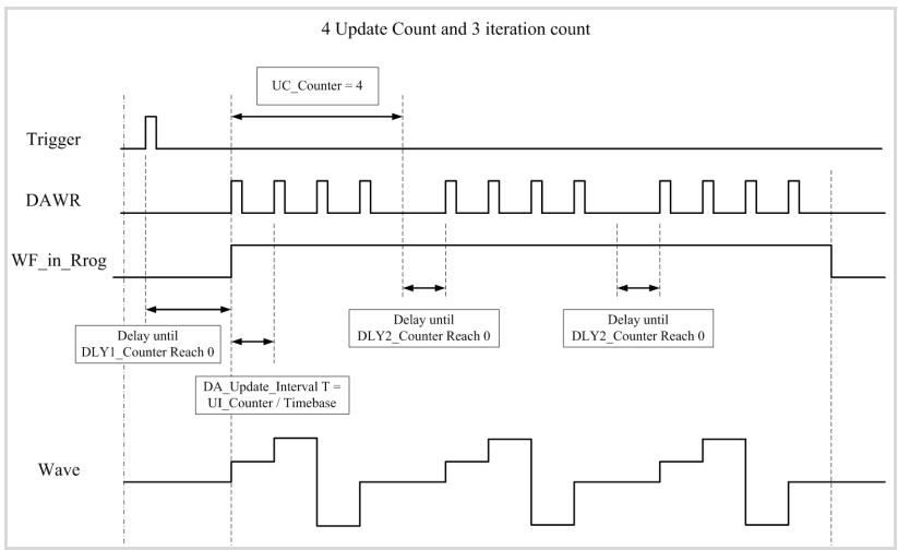
Six counters interact with the waveform to generate different DAWR timing to form various waveforms. These are described in Table 4-2 and illustrated in Figure 4-5.

<table><tr><td>Counter Name</td><td>Width</td><td>Description</td><td>Note</td></tr><tr><td>UI_counter</td><td>32-bit</td><td>Update Interval.Defines the update interval between each data output.</td><td>Update Interval = UI_counter / Timebase*.</td></tr><tr><td>UC_counter</td><td>32-bit</td><td>Update Counts.Defines the number of data in a waveform.</td><td>When value in UC_counter is smaller than the size of waveform patterns, the waveform is generated piece-wisely.</td></tr><tr><td>IC_counter</td><td>32-bit</td><td>Iteration Counts.Defines how many times the waveform is generated.</td><td></td></tr><tr><td>DLY1_counter</td><td>32-bit</td><td>Defines the delay time for waveform generation after the trigger signal.</td><td>Delay Time = (DLY1_counter / Clock Timebase)</td></tr><tr><td>DLY2_counter</td><td>32-bit</td><td>Defines the delay time to separate consecutive waveform generation. This is applicable only in Iterative Waveform Generation mode.</td><td>Delay Time = (DLY2_counter / Clock Timebase)</td></tr><tr><td>Trig_counter</td><td>32-bit</td><td>Defines the acceptable start trigger count when re-trigger function is enabled</td><td></td></tr></table>

Table 4-2: Summary of Counters for Waveform Generation

Timebase $^{*}$ = 80M

# NOTE

The maximum D/A update rate is 1 MHz, and the minimum setting of UI\_counter is 80.
![| Signal          | Event Description                     |\n|-----------------|----------------------------------------|\n| Trigger         | UC_Counter = 4 (Initial)             |\n| DAWR            | Delay until DLY1_Counter Reach 0    |\n| WF_in_Rrog      | Delay until DLY2_Counter Reach 0    |\n| Wave            | DA_Update_Interval T = UI_Counter / Timebase |\n| Transition     | UC_Counter = 4 (Initial)             |\n| Transition     | Delay until DLY1_Counter Reach 0    |\n| Transition     | Delay until DLY2_Counter Reach 0    |\n| Transition     | DA_Update_Interval T = UI_Counter / Timebase |](.pci-6202-manual-4/bfa7b9ed523efff8b1a59e634eb6bbc58c12c5c0d259312a3d76ba96e6f280d1.jpg)

Figure 4-5: Typical D/A Timing of Waveform Generation

# Trigger Modes

# Post-Trigger Generation

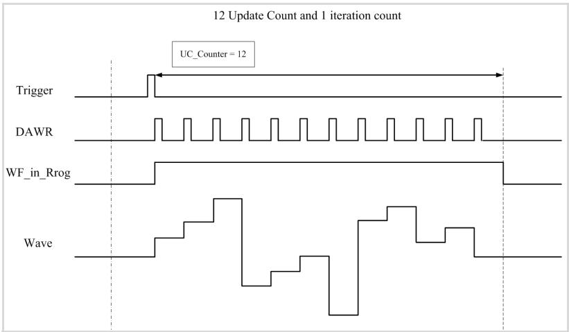
Use post-trigger generation when you want to generate a waveform right after a trigger signal. The number of patterns to be updated after the trigger signal is specified by UC\_counter\* IC\_counter and is illustrated in Figure 4-6.
![| Signal          | Value |\n|-----------------|-------|\n| Trigger         | 12    |\n| DAWR            | 12    |\n| WF_in_Rrog      | 12    |\n| Wave            | 12    |](.pci-6202-manual-4/3c5f6c4bafc1931df7e3dfd3922d8d2342f214afe68bed3a253f0cf3127ffb62.jpg)

Figure 4-6: Post-Trigger Generation

# Delay-Trigger Generation

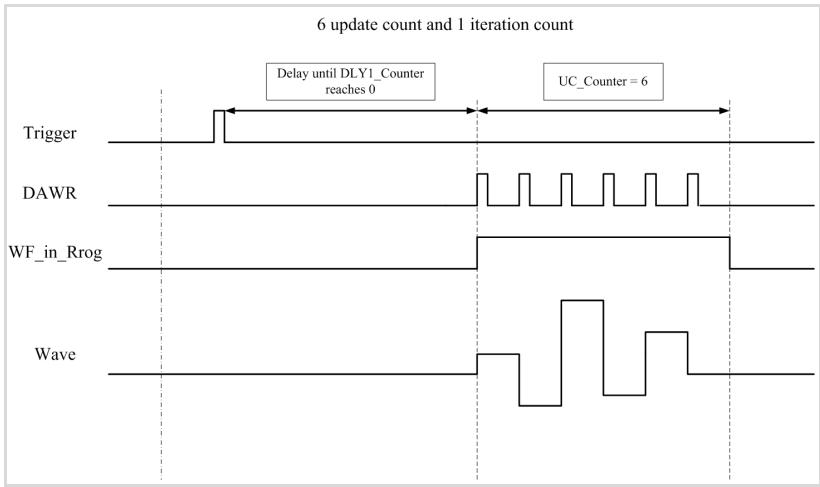
Use delay-trigger when you want to delay the waveform generation after the trigger signal. The delay time is determined by DLY1\_counter, as illustrated in Figure 4-7.

The counter counts down on the rising edges of DLY1\_counter clock source after the start trigger signal. When the count reaches zero, card will start to generate the waveform. The DLY1\_counter clock source can be selected via software application using the internal 80 MHz timebase.
![| Signal          | Value |\n|-----------------|-------|\n| Trigger         | Delay until DLY1 Counter reaches 0 |\n| DAWR            | Uc Counter = 6 |\n| WF_in_Rrog      | Uc Counter = 6 |\n| Wave            | Uc Counter = 6 |](.pci-6202-manual-4/7c902831f530f381da0941847968e120823d319859621cb9f9ff2a22816ea7f5.jpg)

Figure 4-7: Delay-Trigger Generation

# Post-Trigger or Delay-Trigger with Retrigger

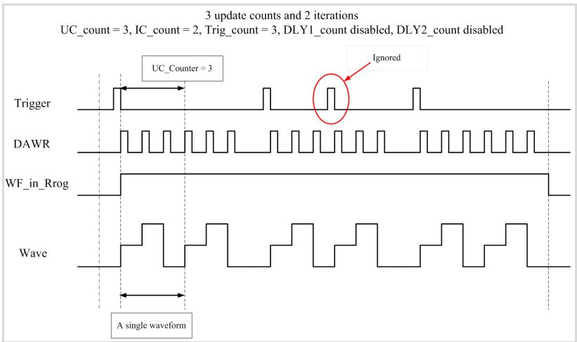
Use post-trigger or delay-trigger with retrigger when you want to generate multiple waveforms with respect to multiple incoming trigger signals. You can set Trig\_counter to specify the number of acceptable trigger signals. Refer to Figure 4-8.

In this example, two waveforms are generated after the first trigger signal. The board then waits for another trigger signal.

When the next trigger signal is asserted, the board generates two more waveforms.

After two trigger signals, as specified in Trig\_Counter, no more triggers signals will be accepted unless trigger reset command is executed. For more information on Iterative Waveform Generation that is used in this example, refer to the next section.
![| Signal          | Value |\n|-----------------|-------|\n| Trigger         | 3     |\n| DAWR            | 3     |\n| WF_in_Rrog      | 3     |\n| Wave            | 3     |](.pci-6202-manual-4/c944212b220db033bf6b6d8f628d048005158789c093aaacbfb04f4c75d27ae7.jpg)

Figure 4-8: Post-Trigger with Retrigger Generation

# NOTE

Start Trigger signals asserted during the waveform generation process will be ignored.

# Iterative Waveform Generation

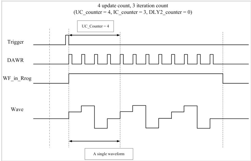
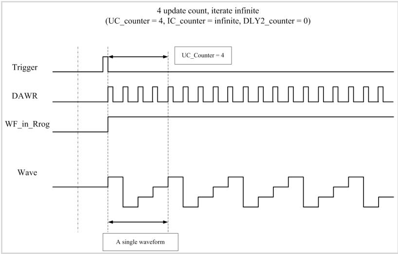
You can set the IC\_counter to generate iterative waveforms no matter which trigger mode is used. The IC\_counter stores the iteration number. Examples are shown in Figure 4-9 and Figure 4-10. When IC\_counter is enabled and set to 0, the waveform generation will not stop until IC\_counter is disabled.

An onboard data FIFO is used to buffer the waveform patterns for waveform generation. If the size of a single waveform is smaller than that of the FIFO, after initially loading the data from the host computer's memory, the data in FIFO will be reused when a single waveform generation is completed and will not occupy the PCI bandwidth afterwards.

However, if the size of a single waveform is larger than that of the FIFO, it needs to be intermittently loaded from the host computer's memory via DMA, and will occupy the PCI bandwidth.
![| Signal          | Value |\n|-----------------|-------|\n| Trigger         | 4     |\n| DAWR            | 4     |\n| WF_in_Rrog      | 4     |\n| Wave            | 4     |](.pci-6202-manual-4/14c8063b33a493fed5bbcbc824ce37d4071cb649653042866e61d966b1880dd9.jpg)

Figure 4-9: Finite Iterative Waveform Generation with Post-trigger

In conjunction with different trigger modes and counter setups, you can manipulate a single waveform to generate different and more complex waveforms.
![| Signal          | Value |\n|-----------------|-------|\n| Trigger         | 4     |\n| DAWR            | 4     |\n| WF_in_Rrog      | 4     |\n| Wave            | 4     |\n| A single waveform | 4     |](.pci-6202-manual-4/b54b4427a5fd969cc6b74ae1eefbea3655dff1b4372df0db71b5586d0ac7d33e.jpg)

Figure 4-10: Infinite Iterative Waveform Generation with Post-trigger

# DLY2 Counter in Iterative Waveform Generation

To expand the flexibility of iterative waveform generation, DLY2\_counter was implemented to separate consecutive waveform generations.

The DLY2\_counter starts counting down right after a single waveform generation is completed. When it reaches zero, the next iteration of waveform generation will start as shown in Figure 4-5. If you generate the waveform piece-wisely, the next piece of waveform will be generated.

# 4.3 General Purpose Digital D/O

The PCI-6202 offers comprehensive support to various digital I/O provided by an FPGA chip. These digital I/O include general purpose digital input and output, PWM, Timer/Counter, and Application Function Interface (AFI).

# General Purpose DIO

PCI-6202 provides 8 channel DI and 8 channel DO. All I/O are static TTL-compliant. You can read/write these I/O line by software polling. In this way, the sample and update rate is fully controlled by software timing.

<table><tr><td>Definition</td><td colspan="2">Pin #</td><td>Definition</td></tr><tr><td>DO0</td><td>1</td><td>35</td><td></td></tr><tr><td>DO1</td><td>2</td><td>36</td><td></td></tr><tr><td>DO2</td><td>3</td><td>37</td><td></td></tr><tr><td>DO3</td><td>4</td><td>38</td><td></td></tr><tr><td>DO4</td><td>5</td><td>39</td><td></td></tr><tr><td>DO5</td><td>6</td><td>40</td><td></td></tr><tr><td>DO6</td><td>7</td><td>41</td><td></td></tr><tr><td>DO7</td><td>8</td><td>42</td><td></td></tr><tr><td>DGND</td><td>9</td><td>43</td><td></td></tr><tr><td>DGND</td><td>10</td><td>44</td><td></td></tr><tr><td>DI0</td><td>11</td><td>45</td><td>DGND</td></tr><tr><td>DI1</td><td>12</td><td>46</td><td>DGND</td></tr><tr><td>DI2</td><td>13</td><td>47</td><td>DGND</td></tr><tr><td>DI3</td><td>14</td><td>48</td><td>DGND</td></tr><tr><td>DI4</td><td>15</td><td>49</td><td>DGND</td></tr><tr><td>DI5</td><td>16</td><td>50</td><td>DGND</td></tr><tr><td>DI6</td><td>17</td><td>51</td><td>DGND</td></tr><tr><td>DI7</td><td>18</td><td>52</td><td>DGND</td></tr><tr><td>DGND</td><td>19</td><td>53</td><td>PWM_0</td></tr><tr><td>DGND</td><td>20</td><td>54</td><td>PWM_1</td></tr><tr><td>DGND</td><td>21</td><td>55</td><td>PWM_2</td></tr><tr><td>DGND</td><td>22</td><td>56</td><td>PWM_3</td></tr><tr><td>DGND</td><td>23</td><td>57</td><td>AFI0</td></tr><tr><td></td><td>24</td><td>58</td><td>AFI1</td></tr><tr><td></td><td>25</td><td>59</td><td>AFI2</td></tr><tr><td></td><td>26</td><td>60</td><td></td></tr><tr><td></td><td>...</td><td>...</td><td></td></tr><tr><td></td><td>34</td><td>68</td><td></td></tr></table>

Table 4-3: TTL DIO Pins in CN1

# Application Function Interface (AFIx)

The application function interface can be used for special functions. The table below shows the available function for each dedicated AFI pin.

# NOTE

When AFlx is configured as one function, these pins may not be used for any other function.

<table><tr><td>Pin</td><td>Function</td><td>Note</td></tr><tr><td rowspan="4">AFI0</td><td>External convert signal out</td><td>Configured as a DA convert source.</td></tr><tr><td>External digital trigger in</td><td>Used for one of all DA output trigger source.</td></tr><tr><td>External digital trigger out</td><td>Export a digital trigger based on a software trigger.</td></tr><tr><td>Encoder position trigger out</td><td>This function is combined with encoder0 input. When encoder counts up for a specific value that you have set, AFI0 will export a digital high signal.</td></tr><tr><td rowspan="4">AFI1</td><td>External convert signal out</td><td>AFI1 can be configured as a DA convert source.</td></tr><tr><td>Digital trigger in</td><td>Used for one of all DA output trigger source.</td></tr><tr><td>Digital trigger out</td><td>Export a digital trigger based on software trigger.</td></tr><tr><td>Encoder position trigger out</td><td>This function is combined with encoder1 input. When encoder counts up for a specific value that you have set, AFI1 will export a digital high signal.</td></tr><tr><td>AFI2</td><td>Encoder position trigger out</td><td>This function is combined with encoder2 input. When encoder counts up for a specific value that you have set, AFI2 will export a digital high signal.</td></tr></table>

Table 4-4: AFI Functions

# PWM Output

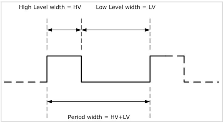
The PCI-6202 provides four dedicated PWM outputs, each consisting of two parameters: high level and low level width. These two parameters have a 24-bit count width that can be used. The PWM base clock is 80MHz.

Figure 4-11 shows the high and low level definition of the PWM output. HV is high level width count value while LV is low level count value.
![High Level width = HV\nLow Level width = LV\nPeriod width = HV+LV](.pci-6202-manual-4/7daeb63ed99831f50d6f2efbd7574ffd940e1c5b8089cb054ca3386dac3f61d9.jpg)

Figure 4-11: PWM Output Parameters

The period width time value is shown in this formula:

$$
P e r i o d \_ t i m e \_ v a l u e = \frac {H V + L V}{8 0 M H z}
$$

HV and LV can also set the PWM duty cycle:

$$
H i g h \_ l e v e l \_ d u t y c y c l e = \frac {H V}{H V + L V}
$$

$$
L o w \_ l e v e l \_ d u t y c y c l e = \frac {L V}{H V + L V}
$$

# General Purpose Timer/Counter

PCI-6202 comes with three general purpose timer/counter sets featuring:

▶ Count up/down controlled by hardware or software
▶ Programmable counter clock source (internal clock up to 80MHz, external clock up to 10MHz)
▶ Programmable gate selection (hardware or software control)
▶ Programmable input and output signal polarities (high active or low active)
▶ Initial Count can be loaded from a software application
▶ Current count value can be read-back by software without affecting circuit operation.

<table><tr><td>Definition</td><td colspan="2">Pin #</td><td>Definition</td></tr><tr><td></td><td>1</td><td>35</td><td>GPTC_OUT0</td></tr><tr><td></td><td>2</td><td>36</td><td>GPTC_GATE0</td></tr><tr><td></td><td>3</td><td>37</td><td>GPTC_UD0</td></tr><tr><td></td><td>4</td><td>38</td><td>GPTC_AUX0</td></tr><tr><td></td><td>5</td><td>39</td><td>GPTC_CLK0</td></tr><tr><td></td><td>6</td><td>40</td><td>GPTC_OUT1</td></tr><tr><td></td><td>7</td><td>41</td><td>GPTC_GATE1</td></tr><tr><td></td><td>8</td><td>42</td><td>GPTC_UD1</td></tr><tr><td>DGND</td><td>9</td><td>43</td><td>GPTC_AUX1</td></tr><tr><td>DGND</td><td>10</td><td>44</td><td>GPTC_CLK1</td></tr><tr><td></td><td>11</td><td>45</td><td>DGND</td></tr><tr><td></td><td>12</td><td>46</td><td>DGND</td></tr><tr><td></td><td>13</td><td>47</td><td>DGND</td></tr><tr><td></td><td>14</td><td>48</td><td>DGND</td></tr><tr><td></td><td>15</td><td>49</td><td>DGND</td></tr><tr><td></td><td>16</td><td>50</td><td>DGND</td></tr><tr><td></td><td>17</td><td>51</td><td>DGND</td></tr><tr><td></td><td>18</td><td>52</td><td>DGND</td></tr><tr><td>DGND</td><td>19</td><td>53</td><td></td></tr><tr><td>DGND</td><td>20</td><td>54</td><td></td></tr><tr><td>DGND</td><td>21</td><td>55</td><td></td></tr><tr><td>DGND</td><td>22</td><td>56</td><td></td></tr><tr><td>DGND</td><td>23</td><td>57</td><td></td></tr><tr><td>...</td><td>...</td><td>...</td><td>...</td></tr><tr><td></td><td>34</td><td>68</td><td></td></tr></table>

Table 4-5: Timer/Counter Mode Pins in CN1

# Basic Timer/Counter Functions

Each timer/counter has three inputs that can be controlled via hardware or software applications. They are clock input (GPTC\_CLK), gate input (GPTC\_GATE), and up/down control input (GPTC\_UD). The GPTC\_CLK input provides a clock source input to the timer/counter. Active edges on the GPTC\_CLK input make the counter increment or decrement. The GPTC\_UD input controls the counter to count up or down (high: count up; low: count down), while the GPTC\_GATE input is a control signal which acts as a counter enable or a counter trigger signal under different applications. The GPTC\_OUT will then generate a pulse signal based on which timer/counter mode you have set.

All input/output signals polarities can be programmed by software application. For brevity, all GPTC\_CLK, GPTC\_GATE, and GPTC\_OUT in the following illustrations are assumed to be active high or rising-edge triggered.

# General Purpose Timer/Counter modes

Ten programmable timer/counter modes are provided. All modes start operating following a software-start signal that is set by the software. The GPTC software reset initializes the status of the counter and reloads the initial value to the counter. The operation remains halted until the software-start is executed again. The operating theories under different modes are described in the following sections.

# Mode1: Simple Edge Counting

In this mode, the counter counts the number of pulses on the GPTC\_CLK after the software-start. Initial count can be loaded from the software application. Current count value can be read-back by software any time with no effect to the counting. GPTC\_GATE is used to enable/disable counting. When GPTC\_GATE is inactive, the counter halts the current count value. Figure 4-12 illustrates the operation with initial count = 5, count-down mode.

![| Signal | Value |\n|--------|-------|\n| Gate   | 5     |\n| CLK    | 5     |](.pci-6202-manual-4/2893a174498acb113b64f5cd6095fae286a5318e268cb49450103352bb68ec3b.jpg)

Figure 4-12: Mode 1 Operation

# Mode 2: Single Period Measurement

The counter counts the period of the signal on GPTC\_GATE in terms of GPTC\_CLK. Initial count can be loaded from the software application. After the software-start, the counter counts the number of active edges on GPTC\_CLK between two active edges of GPTC\_GATE. After the completion of the period interval on GPTC\_GATE, GPTC\_OUT outputs high and then current count value can be read-back by the software application. Figure 4-13 illustrates the operation where initial count = 0, count-up mode.

![Software start\nGate\nCLK\nCount value\n0 0 1 2 3 4 5 5 5](.pci-6202-manual-4/0d6574fcde92302af6a95158b16ac88d1ecc8d847a13baba78cd91c1fcfaaf28.jpg)

Figure 4-13: Mode 2 Operation

# Mode 3: Single Pulse-width Measurement

The counter counts the pulse-width of the signal on GPTC\_GATE in terms of GPTC\_CLK. Initial count can be loaded from the software application.

After the software-start, the counter counts the number of active edges on GPTC\_CLK when GPTC\_GATE is in its active state. After the completion of the pulse-width interval on

GPTC\_GATE, GPTC\_OUT outputs high and then current count value can be read-back by the software application. Figure 4-14 illustrates the operation where initial count = 0, count-up mode.

![Software start\nGate\nCLK\nCount value\n0 0 1 2 3 4 5 5 5](.pci-6202-manual-4/d779ca58ad1951ac201ae07623283c5a94d14304e5477be7c18f4bc55ddd14bf.jpg)

Figure 4-14: Mode 3 Operation

# Mode 4: Single Gated Pulse Generation

This generates a single pulse with programmable delay and programmable pulse-width following the software-start. The two programmable parameters can be specified in terms of periods of the GPTC\_CLK input by the software application. GPTC\_GATE is use to enable/disable counting. When GPTC\_GATE is inactive, the counter halts the current count value. Figure 4-15 illustrates the generation of a single pulse with a pulse delay of two and a pulse-width of four.

![| Signal     | Value |\n|------------|-------|\n| Gate       | High  |\n| CLK        | Low   |\n| Count value| 2     |\n| OUT        | 0     |](.pci-6202-manual-4/74dc7613e8048110f1a4e155a8e5321397b5600f93af7a81afc24623eeb5d7ec.jpg)

Figure 4-15: Mode 4 Operation

# Mode 5: Single Triggered Pulse Generation

This mode generates a single pulse with programmable delay and programmable pulse-width following an active GPTC\_GATE edge. You may specify these programmable parameters in terms of periods of the GPTC\_CLK input. When the first GPTC\_GATE edge triggers the single pulse, GPTC\_GATE makes no effect until the software-start is executed again. Figure 4-16 illustrates the generation of a single pulse with a pulse delay of two and a pulse-width of four.

![| Time | Gate | CLK | Count value |\n|------|------|-----|-------------|\n| 0    |      |     |             |\n| 1    |      |     |             |\n| 2    |      |     |             |\n| 3    |      |     |             |\n| 4    |      |     |             |](.pci-6202-manual-4/261dcd271a10ad56420a63e102db030949ceaf3428426c8a42c0c09701cc6482.jpg)

Figure 4-16: Mode 5 Operation

# Mode 6: Re-triggered Single Pulse Generation

This mode is similar to Mode 5 except that the counter generates a pulse following every active edge of GPTC\_GATE. After the software-start, every active GPTC\_GATE edge triggers a single pulse with programmable delay and pulse-width. Any GPTC\_GATE triggers that occur when the prior pulse is not completed is ignored. Figure 4-17 illustrates the generation of two pulses with a pulse delay of two and a pulse-width of four.

![| Signal | Value |\n|--------|-------|\n| Gate   | 0     |\n| CLK    | 0     |\n| Count value | 2 |\n| OUT    | 0     |](.pci-6202-manual-4/c5db3a3c74e023e4ed2fc9379a3a04482d7dc27937c74548b80d60f6860ea953.jpg)

Figure 4-17: Mode 6 Operation

# Mode 7: Single Triggered Continuous Pulse Generation

This mode is similar to Mode 5 except that the counter generates continuous periodic pulses with programmable pulse interval and pulse-width following the first active edge of GPTC\_GATE. When the first GPTC\_GATE edge triggers the counter, GPTC\_GATE makes no effect until the software-start is executed again. Figure 4-18 illustrates the generation of two pulses with a pulse delay of four and a pulse-width of three.

![Software start\nGate\nCLK\nCount value\nOUT](.pci-6202-manual-4/58ebe2083e9f8ecf40923a45a8311fdf34b947b87b096fe0e192fd3431c4ae3f.jpg)

Figure 4-18: Mode 7 Operation

# Mode 8: Continuous Gated Pulse Generation

This mode generates periodic pulses with programmable pulse interval and pulse-width following the software-start. GPTC\_GATE is use to enable/disable counting. When GPTC\_GATE is inactive, the counter halts the current count value. Figure 4-19 illustrates the generation of two pulses with a pulse delay of four and a pulse-width of three.

![Software start\nGate\nCLK\nCount value 4 1 1 1 1 0 3 1 0 1 1 1 0 2 1 1 0 1\nOUT](.pci-6202-manual-4/eabb27c8b49c771f391632bea510e9f7292784f9c8f08e27cc522b7be91e2dca.jpg)

Figure 4-19: Mode 8 Operation

# Mode 9: Edge Separation Measurement

Measures the time differentiation between two different pulse signals. The first pulse signal is connected to GPTC\_GATE and the second signal is connected to GPTC\_AUX. It counts the clocks that pass by between the rising edge signal of two different pulses through the 40MHz internal clock or external clock. You can calculate the time period via the known clock frequency. The maximum counting width is 32-bit. Figure 4-20 illustrates how the counter value decreases in Edge Separation Measurement mode.

![| Signal | Value |\n|--------|-------|\n| Gate   | 11    |\n| Gate   | 12    |\n| Gate   | 13    |\n| Gate   | 14    |\n| Gate   | 15    |\n| Gate   | 16    |\n| Gate   | 17    |\n| Gate   | 18    |\n| Gate   | 19    |\n| Gate   | 20    |\n| AUX    | 11    |\n| AUX    | 12    |\n| AUX    | 13    |\n| AUX    | 14    |\n| AUX    | 15    |\n| AUX    | 16    |\n| AUX    | 17    |\n| AUX    | 18    |\n| AUX    | 19    |\n| AUX    | 20    |\n| CLK    | 11    |\n| CLK    | 12    |\n| CLK    | 13    |\n| CLK    | 14    |\n| CLK    | 15    |\n| CLK    | 16    |\n| CLK    | 17    |\n| CLK    | 18    |\n| CLK    | 19    |\n| CLK    | 20    |\n| Count value | 11   |\n| Count value | 12   |\n| Count value | 13   |\n| Count value | 14   |\n| Count value | 15   |\n| Count value | 16   |\n| Count value | 17   |\n| Count value | 18   |\n| Count value | 19   |\n| Count value | 20   |](.pci-6202-manual-4/0324cff28f3911906b818c5d18a57c903ebc3fe2a8e0f2a5681ffe7cc695ebe8.jpg)

Figure 4-20: Mode 9 Operation

# Mode 10: PWM Output

Aside from the 4-CH dedicated PWM outputs, the card's powerful timer/counter can also simulate a PWM (Pulse Width Modulation) output. By setting varying number of Pulse\_initial\_cnt and Pulse\_length\_cnt, you can get varying pulse frequency (Fpwm) and duty cycle (Dutypwm). Figure 4-21 illustrates the PWM output and the formula showing how to calculate the PWM frequency and duty cycle.

![PWMOUT\nTIMEBASE\nPulse_Initial_cnt =0x7\nPulse_length_cnt =0x8](.pci-6202-manual-4/80bbd0bb8b9530c6b5fccd4160a0a3d852c768b803c6fcf2f9f36d15449f91ad.jpg)

Figure 4-21: Mode 10 Operation

$$
\begin{array}{l} F _ {P W M} = \frac {F _ {\text { Timebase }}}{\text { Pulse } \_ i n i t i a l \_ c n t + \text { Pulse } \_ l e n g t h \_ c n t} \\ D u t y _ {P W M} = \frac {\text { Pulse\_length\_cnt }}{\text { Pulse\_initial\_cnt } + \text { Pulse\_length\_cnt }} \\ \end{array}
$$

# 4.4 Isolation Encoder

PCI-6202 features a combination of data acquisition and simple motion control with support for three encoder input sets which provide an alternative for step motor or servo motor's position feedback. The internal isolation provides easy encoder connection. The encoder sets are assigned in CN2.

<table><tr><td>Definition</td><td colspan="2">Pin #</td><td>Definition</td></tr><tr><td></td><td>1</td><td>35</td><td></td></tr><tr><td></td><td>2</td><td>36</td><td></td></tr><tr><td></td><td>3</td><td>37</td><td></td></tr><tr><td></td><td>4</td><td>38</td><td></td></tr><tr><td></td><td>5</td><td>39</td><td></td></tr><tr><td></td><td>6</td><td>40</td><td></td></tr><tr><td></td><td>7</td><td>41</td><td></td></tr><tr><td></td><td>8</td><td>42</td><td></td></tr><tr><td>COM</td><td>9</td><td>43</td><td>COM</td></tr><tr><td>COM</td><td>10</td><td>44</td><td>COM</td></tr><tr><td>EA0+</td><td>11</td><td>45</td><td>EA1+</td></tr><tr><td>EA0-</td><td>12</td><td>46</td><td>EA1-</td></tr><tr><td>EB0+</td><td>13</td><td>47</td><td>EB1+</td></tr><tr><td>EB0-</td><td>14</td><td>48</td><td>EB1-</td></tr><tr><td>EZ0+</td><td>15</td><td>49</td><td>EZ1+</td></tr><tr><td>EZ0-</td><td>16</td><td>50</td><td>EZ1-</td></tr><tr><td>EORG0</td><td>17</td><td>51</td><td>EORG1</td></tr><tr><td>EA2+</td><td>18</td><td>52</td><td>EZ2+</td></tr><tr><td>EA2-</td><td>19</td><td>53</td><td>EZ2-</td></tr><tr><td>EB2+</td><td>20</td><td>54</td><td>EORG2</td></tr><tr><td>EB2-</td><td>21</td><td>55</td><td>Ext. 24V</td></tr><tr><td>Ext. GND</td><td>22</td><td>56</td><td>Ext. 24V</td></tr><tr><td>IGND</td><td>23</td><td>57</td><td>Ext. GND</td></tr><tr><td>IGND</td><td>24</td><td>58</td><td>IGND</td></tr><tr><td>VDD</td><td>25</td><td>59</td><td>IGND</td></tr><tr><td>VDD</td><td>26</td><td>60</td><td></td></tr><tr><td></td><td>27</td><td>61</td><td></td></tr><tr><td></td><td>28</td><td>62</td><td></td></tr><tr><td></td><td>29</td><td>63</td><td></td></tr><tr><td></td><td>30</td><td>64</td><td></td></tr><tr><td></td><td>31</td><td>65</td><td></td></tr><tr><td></td><td>32</td><td>66</td><td></td></tr><tr><td></td><td>33</td><td>67</td><td></td></tr><tr><td></td><td>34</td><td>68</td><td></td></tr></table>

Table 4-6: Encoder Pins in CN2

# Encoder Isolation Input Module

Figure 4-22 illustrates the encoder isolation phase A, phase B and phase Z inputs module with 2500 Vrms protection.

![Based on the provided flowchart/block diagram, here are the labeled blocks and their connections:\n\n**Labeled Blocks:**\n*   **Encoder phase A+, phase B+, phase Z+ Input**\n*   **470 ohm Resistor** (a light blue rectangle)\n*   **Central Rectangular Block** (containing a downward-pointing diode/LED symbol with arrows pointing right, and a right-pointing inverter symbol with a circle at the tip)\n*   **Internal logic Power** (connected via a circle terminal)\n*   **Internal Signal to FPGA**\n*   **Encoder phase A-, phase B-, phase Z- Input**\n*   **Internal Ground** (connected via a ground symbol)\n\n**Connections:**\n*   **Encoder phase A+, phase B+, phase Z+ Input** connects via a double arrow to the **470 ohm Resistor**.\n*   The **470 ohm Resistor** connects via a line to the top input of the central rectangular block.\n*   **Internal logic Power** connects via a line to the top wire of the central rectangular block.\n*   **Internal Signal to FPGA** is connected via an arrow to the output of the inverter symbol inside the central rectangular block.\n*   **Internal Ground** connects via a ground symbol to the bottom wire of the central rectangular block.\n*   **Encoder phase A-, phase B-, phase Z- Input** connects via a double arrow to the bottom input of the central rectangular block.](.pci-6202-manual-4/302daace6249fc23536b8ec199dea657ed728c97e84527deb52ba981c67c50a1.jpg)

Figure 4-22: Encoder Isolation Input Module

The Encoder OGRx input is different from the encoder phase input since you need to add an external +24V power to drive the photo-couple. Figure 4-23 shows the OGRx input.

![Based on the provided diagram, here are the labeled blocks and their connections:\n\n**Labeled Blocks:**\n*   External +24V power\n*   4.7K Resistor\n*   Encoder ORGx\n*   Internal logic Power\n*   Internal Signal to FPGA\n*   Internal Ground\n*   A central square block containing a diode symbol and an inverter symbol (triangle with a circle).\n\n**Connections:**\n*   **External +24V power** connects to the top of the **4.7K Resistor**.\n*   The bottom of the **4.7K Resistor** connects to the upper input terminal of the central square block.\n*   **Encoder ORGx** connects to the lower input terminal of the central square block.\n*   Inside the central block, optical arrows indicate a connection between the diode symbol and the inverter symbol.\n*   The top right corner of the central square block connects to **Internal logic Power**.\n*   The output of the inverter symbol (indicated by an arrow) connects to **Internal Signal to FPGA**.\n*   The bottom right corner of the central square block connects to **Internal Ground**.](.pci-6202-manual-4/86bb9fd8cfaac8bbccf5c3c27fb0806aa747598a0fb3b6677721a610f4bcc3e0.jpg)

Figure 4-23: Encoder OGRx Input

# CW/CCW Encoder Mode

When GPTC is set to CW/CCW encoder mode and when the input EAx is connected to CW source signal and EBx is connected to CCW source signal, pulses from EAx will cause the counter to counter up and spin the motor clockwise. Otherwise, pulses from EBx will cause the counter to counter down and spin the motor counterclockwise. Figure 4-24 shows the increase/decrease of counter value in CW or CCW encoder mode.

![CW\nCCW\nEA0/EA1\nEB0/EB1\nCount Value 0 1 2 3 4 5 6 7 8 9 7 6 5 4 3 2](.pci-6202-manual-4/c77c0ff77f3024514ed61cab4a5b117e2ef06d30fbef86d91367d363a9922a1e.jpg)

Figure 4-24: CW/CCW Encoder Timing

# X1 Encoder Mode

In X1 encoder mode, if phase A (EA0/EA1) is advanced of phase B (EB0/EB1) in a quadrature cycle, the increment of counter value will be 1. Otherwise, if phase B is advanced of phase A in a quadrature cycle, the decrement of counter value will also be 1.

Figure 4-25 shows a quadrature cycle and the increment and decrement of counter value in X1 encoder mode. When phase A leads phase B, the counter value increases on the first rising edge of CLK after phase A goes high. When phase B leads phase A, the counter value decreases on the first rising edge of CLK after phase A goes low.

![Phase A\nPhase B\nCLK\nCount Value 0 1 1 2 2 3 3 2 2 1](.pci-6202-manual-4/b10c44b1825607dda94e18d50012afb29d98568f26fbf42c22cc07c475956d9e.jpg)

Figure 4-25: X1 Encoder Mode

# X2 Encoder Mode

This mode is similar to X1 Encoder Mode, except that the amount of counter value increases or decreases by two. Refer to Figure 4-26.

![Phase A\nPhase B\nCLK\nCount Value 0 1 2 3 4 5 5 4 3 2 1](.pci-6202-manual-4/fb9b864479efa6d5f655982e5cb1c2e4adcf846f69e5c7b84b14d92f274ee15f.jpg)

Figure 4-26: X2 Encoder Mode

# X4 Encoder Mode

This mode is similar to X1 Encoder Mode, except that the amount of counter value increases or decreases by four. Refer to Figure 4-27.

![| Time | Phase A | Phase B | CLK |\n|------|---------|---------|-----|\n| 0    | Yes     | No      | No  |\n| 1    | Yes     | No      | No  |\n| 2    | Yes     | No      | No  |\n| 3    | Yes     | No      | No  |\n| 4    | Yes     | No      | No  |\n| 5    | Yes     | No      | No  |\n| 6    | Yes     | No      | No  |\n| 7    | Yes     | No      | No  |\n| 8    | Yes     | No      | No  |\n| 9    | Yes     | No      | No  |\n| 0    | Yes     | No      | No  |\n| 1    | Yes     | No      | No  |\n| 2    | Yes     | No      | No  |\n| 3    | Yes     | No      | No  |\n| 4    | Yes     | No      | No  |\n| 5    | Yes     | No      | No  |\n| 6    | Yes     | No      | No  |\n| ...  | ...     | ...     | ... |\n| 9    | Yes     | Yes     | Yes |\n| 8    | Yes     | Yes     | Yes |\n| 7    | Yes     | Yes     | Yes |\n| 6    | Yes     | Yes     | Yes |\n| 5    | Yes     | Yes     | Yes |\n| 4    | Yes     | Yes     | Yes |\n| 3    | Yes     | Yes     | Yes |\n| 2    | Yes     | Yes     | Yes |\n| 1    | Yes     | Yes     | Yes |\n| 0    | Yes     | Yes     | Yes |](.pci-6202-manual-4/3cdbcc4824ef0f70767a31f2af299bf87115708fe1c9e86c45eaacd00331248f.jpg)

Figure 4-27: X4 Encoder Mode

# Phase Z

Each encoder mode may use a third phase, phase Z, that is also frequently used for the index phase. You may decide if the counter needs to be reloaded a specified value when phase Z is at a logic high level with phase A and B at a specific logic condition.

You must ensure that the logic level of phase Z is high during at least a portion of the phase you specify for reload when you use phase Z. Otherwise, the counter does not reload.

In Figure 4-28, the reload phase is when the logic level of phase A is high, phase B is low, and phase Z is high in X1

Encoder Mode. In addition, reloading takes higher priority than increment or decrement of counter value. The reload occurs within one maximum CLK period after the reload phase becomes true. After the counter value is reloaded, the counter continues to count as before.

![| Phase | Value |\n|-------|-------|\n| Phase A | 0 |\n| Phase A | 1 |\n| Phase A | 2 |\n| Phase A | 3 |\n| Phase B | 0 |\n| Phase B | 1 |\n| Phase B | 2 |\n| Phase B | 3 |\n| Phase Z | 0 |\n| Phase Z | 1 |\n| Phase Z | 2 |\n| Phase Z | 3 |\n| CLK | 0 |\n| CLK | 1 |\n| CLK | 2 |\n| CLK | 3 |](.pci-6202-manual-4/e83b65801f2c0dc89f1e39e93162fb024b85fed2b67690a0067fa316a43f0a8e.jpg)

Figure 4-28: Phase Z

# Original Signal (ORGx)

Original Signal (ORG0/ORG2/ORG1) is used with phase Z. With ORG enabled, a high level on phase Z and ORG causes the counter to reload with a specified value in a specified phase of the quadrature cycle. When you use ORG signal if it is at a low level and phase Z is at a high level, then counter reload is ignored.

# Encoder Position Trigger

The PCI-6202 comes with a special encoder function. This function combines the encoder count function, digital output and system interrupt. When you set the pacer number and enable the encoder position trigger function, this function will start to count.

When the counting number is equal to the multiple of pacer number, the position trigger will output high in AFlx pin or generate an interrupt for software operation. The behavior may be selected by configuring this function. The output AFlx pulse width can still be configured as 200 $\mu$ s, 2ms, 20ms and 200ms by the software application.

# 4.5 Isolated Digital Output

The isolated digital output circuit offers an open collector-type output and an isolation voltage of 2500 Vrms between the isolated output and the host power signals. Refer to Figure 4-29.

![Internal 3.3V\nPull-up Resistor\nInternal Signal to FPGA\nIsolator\nExternal Isolation Power\nIsolation +5V\nMOS\nIsolation DOx\nLOAD\nIGND](.pci-6202-manual-4/1c77ff98cde03b27914a698c33d812a2f06f78f092fad659d5a97a3aad3201d3.jpg)

Figure 4-29: Isolated Digital Output

# 4.6 Isolated Digital Input

The isolated digital input circuit is equipped with a current-limit resistor and supports an input voltage of up to 24V. The isolation voltage between the isolated input and the host power signals is 2500 Vrms, as illustrated in Figure 4-30.

![Isolation DI\n4.7K ohm Resistor\nCOM\nIsolator\n+3.3V\nPull-up Resistor\nSignal to FPGA\nGround](.pci-6202-manual-4/eebb278a009eeca5e5ffce79acc1129c5cd360c8f3f7d1fd2bdb4619aa237780.jpg)

Figure 4-30: Isolated Digital Input

# NOTE

The 4.7 kΩ resistor constrains the maximum isolated digital input current.

# 4.7 Trigger Sources

The PCI-6202 supports two trigger sources for analog input: software trigger and external digital trigger.

# Software Trigger

This trigger mode does not need any external trigger source. The trigger asserts right after you execute the specified function calls to begin data acquisition.

# External Digital Trigger

An external digital trigger occurs when a rising edge or a falling edge is detected on the digital signal connected to the PCI-6202's function I/O. You can set any DI line as external trigger pin. You may also easily program the trigger polarity via the ADLINK software drivers. Take note that the signal level of the external digital trigger signals should be TTL-compatible with a minimum 25 ns pulse.

![The image displays two separate waveform diagrams illustrating signal triggers.\n\n**Left Diagram:**\n*   **Visual:** A waveform signal rising vertically.\n*   **Connection:** An upward-pointing arrow is positioned along the rising edge.\n*   **Label:** The text 'Positive-edge trigger event occurs' is located to the left of the rising edge.\n\n**Right Diagram:**\n*   **Visual:** A waveform signal falling vertically.\n*   **Connection:** A downward-pointing arrow is positioned along the falling edge.\n*   **Label:** The text 'Negative-edge trigger event occurs' is located to the right of the falling edge.](.pci-6202-manual-4/44c7312eb14d6daf5ea1d6c4c01708a75fca31a9d3b834f57034655f98d5cf5a.jpg)

Figure 4-31: External Digital Trigger

# 5 Calibration

Before shipment, the PCI-6202 is factory calibrated with Agilent 34410. The calibration is done by writing the associated calibration constants of TrimDACs firmware to the onboard EEPROM. TrimDACs firmware is the algorithm in the FPGA. Loading calibration constants is the process of loading the values of TrimDACs firmware stored in the onboard EEPROM.

# NOTE

A one year re-calibration interval is recommended.

Contact your distributor or ADLINK to have your card recalibrated.

# Warranty Policy

Thank you for choosing ADLINK. To understand your rights and enjoy all the after-sales services we offer, please read the following carefully.

1. Before using ADLINK's products please read the user manual and follow the instructions exactly. When sending in damaged products for repair, please attach an RMA application form which can be downloaded from: http://rma.adlinktech.com/policy/.
2. All ADLINK products come with a limited two-year warranty, one year for products bought in China:

The warranty period starts on the day the product is shipped from ADLINK's factory.
▶ Peripherals and third-party products not manufactured by ADLINK will be covered by the original manufacturers' warranty.
For products containing storage devices (hard drives, flash cards, etc.), please back up your data before sending them for repair. ADLINK is not responsible for any loss of data.
▶ Please ensure the use of properly licensed software with our systems. ADLINK does not condone the use of pirated software and will not service systems using such software. ADLINK will not be held legally responsible for products shipped with unlicensed software installed by the user.
For general repairs, please do not include peripheral accessories. If peripherals need to be included, be certain to specify which items you sent on the RMA Request & Confirmation Form. ADLINK is not responsible for items not listed on the RMA Request & Confirmation Form.

3. Our repair service is not covered by ADLINK's guarantee in the following situations:

▶ Damage caused by not following instructions in the User's Manual.
▶ Damage caused by carelessness on the user's part during product transportation.
▶ Damage caused by fire, earthquakes, floods, lightening, pollution, other acts of God, and/or incorrect usage of voltage transformers.
▶ Damage caused by unsuitable storage environments (i.e. high temperatures, high humidity, or volatile chemicals).
▶ Damage caused by leakage of battery fluid during or after change of batteries by customer/user.
▶ Damage from improper repair by unauthorized ADLINK technicians.
▶ Products with altered and/or damaged serial numbers are not entitled to our service.
▶ This warranty is not transferable or extendible.
▶ Other categories not protected under our warranty.

4. Customers are responsible for shipping costs to transport damaged products to our company or sales office.

5. To ensure the speed and quality of product repair, please download an RMA application form from our company website: http://rma.adlinktech.com/policy. Damaged products with attached RMA forms receive priority.

If you have any further questions, please email our FAE staff: service@adlinktech.com.
[🔗 Link to the original document](.pci-6202-manual-4/pci-6202-manual-4.pdf)
