# NuDAQ® PCI-9112

# Multi-function DAS Card for

# PCI / 3U CompactPCI

User's Manual

Manual Revision: 4.0

Revision Date: March 16, 2022

Part No: 50M-00070-1000

# Revision History

<table><tr><td>Revision</td><td>Release Date</td><td>Description of Change(s)</td></tr><tr><td>3.90</td><td>Jan. 24, 2003</td><td>Updated release</td></tr><tr><td>4.0</td><td>March 16, 2022</td><td>Product update release</td></tr></table>

# Preface

Copyright © 2022 ADLINK Technology, Inc.

This document contains proprietary information protected by copyright. All rights are reserved. No part of this manual may be reproduced by any mechanical, electronic, or other means in any form without prior written permission of the manufacturer.

# Disclaimer

The information in this document is subject to change without prior notice in order to improve reliability, design, and function and does not represent a commitment on the part of the manufacturer.

In no event will the manufacturer be liable for direct, indirect, special, incidental, or consequential damages arising out of the use or inability to use the product or documentation, even if advised of the possibility of such damages.

# Environmental Responsibility

ADLINK is committed to fulfill its social responsibility to global environmental preservation through compliance with the European Union's Restriction of Hazardous Substances (RoHS) directive and Waste Electrical and Electronic Equipment (WEEE) directive. Environmental Protection is a top priority for ADLINK. We have enforced measures to ensure that our products, manufacturing processes, components, and raw materials have as little impact on the environment as possible. When products are at their end of life, our customers are encouraged to dispose of them in accordance with the product disposal and/or recovery programs prescribed by their nation or company.

# Trademarks

Product names mentioned herein are used for identification purposes only and may be trademarks and/or registered trademarks of their respective companies.

# Conventions

Take note of the following conventions used throughout this manual to make sure that users perform certain tasks and instructions properly.

![The image displays an icon of a white document with a folded top-left corner. Faint horizontal gray lines run across the page. A large, thick red checkmark is superimposed over the document, positioned diagonally from the lower left to the upper right.](.pci-9112-50m-00070-1000-40/dd9d3f15bc8c2e7860e67765875a764621889547d84ba782c7f6d6e556d8957c.jpg)
NOTE:

Additional information, aids, and tips that help users perform tasks.

![The image displays a standard yellow triangular caution sign with a thick black border. In the center of the triangle is a large black exclamation mark.](.pci-9112-50m-00070-1000-40/72dc39bbe8a805d88e088c00291d08c12c4297d46b373a26ab26ced75a1d07ec.jpg)
CAUTION:

Information to prevent minor physical injury, component damage, data loss, and/or program corruption when trying to complete a task.

![The image displays a red triangle containing a large white exclamation point in its center.](.pci-9112-50m-00070-1000-40/1a9436ded069856fd1f53c8d306ff320d56c018aaf6bbdffddcccd295cf0fb11.jpg)
WARNING:

Information to prevent serious physical injury, component damage, data loss, and/or program corruption when trying to complete a specific task.

# Table of Contents

# Revision History...... ii

# Preface.... iii

# 1 Introduction ...... 1

1.1 Features.... 1
1.2 Applications 2
1.3 Specifications.... 3
1.4 Software Support 5

# 2 Getting Started 9

2.1 Package Contents 10
2.2 Device Layout and I/O Connectors 11
2.3 Jumper Settings.... 12
2.4 Connector Pin Assignments 16
2.5 Hardware Installation Outline.... 19
2.6 Device Installation for Windows Systems 21
2.7 Daughter Board Connection 22

# 3 Operation Theory 25

3.1 A/D Conversion.... 25
3.2 Analog Input Signal Connection 26
3.3 D/A Conversion.... 32
3.4 Digital Input and Output 33
3.5 Timer/Counter Operation 34

# Important Safety Instructions 37

# Getting Service.... 41

This page intentionally left blank.

# 1 Introduction

The PCI-9112 is a 12-bit, 110KHz, multifunction DAS data acquisition card. The PCI-9112 DAS card uses state-of-the-art technology, making it ideal for data logging and signal analysis applications in medicine, process control, etc.

# 1.1 Features

The PCI-9112 provides the following advanced features:

▶ 32-bit PCI bus
▶ 12-bit analog input resolution
▶ Onboard A/D FIFO memory
▶ Auto-scanning channel selection
▶ Up to 110KHz A/D sampling rates
▶ 16 single-ended or 8 differential analog input channels
▶ Bipolar or Unipolar input signals
▶ Programmable Gain Control (x0.5, x1, x2, x4, x8)
▶ Two 12-bit monolithic multiplying analog output channels
▶ 16 digital output channels
▶ 16 digital input channels
▶ 3 independent programmable 16-bit down counters
- Three A/D trigger modes: software trigger, programmable pacer trigger, and external pulse trigger.
▶ Integrated DC-to-DC converter for stable analog power source
▶ 37-pin D-type connector

# 1.2 Applications

▶ Industrial and laboratory ON/OFF control
▶ Energy management
▶ Annunciation
▶ Security controller
▶ Product testing
▶ Event and frequency counting
▶ Waveform and pulse generation
▶ BCD interface driver

# 1.3 Specifications

<table><tr><td colspan="4">Analog Input (A/D)</td></tr><tr><td>Converter</td><td colspan="3">ADS8922 or equivalent, successive approximation type</td></tr><tr><td>Resolution</td><td colspan="3">12-bit</td></tr><tr><td>Input Channels</td><td colspan="3">16 Single-ended or 8 Differential</td></tr><tr><td>Input Range(Programmable)</td><td colspan="3">Bipolar: ±10V, ±5V, ±2.5V, ±1.25V, ±0.625VUnipolar: 0-10V, 0-5V, 0-2.5V, 0-1.25V</td></tr><tr><td>Conversion Time</td><td colspan="3">2 μ sec</td></tr><tr><td>Throughput</td><td colspan="3">110KHz multiplexing (maximum)</td></tr><tr><td>Analog Input Over-voltage Protection</td><td colspan="3">Continuous ±35V max.</td></tr><tr><td rowspan="6">Accuracy</td><td>Gain</td><td>Range</td><td>Accuracy (mv)</td></tr><tr><td>1</td><td>±10v</td><td>±1.8966</td></tr><tr><td>2</td><td>±5v</td><td>±0.8626</td></tr><tr><td>4</td><td>±2.5v</td><td>±0.4445</td></tr><tr><td>8</td><td>±1.25v</td><td>±0.3282</td></tr><tr><td>16</td><td>±0.625v</td><td>±0.1380</td></tr><tr><td>Input Impedance</td><td colspan="3">10 MΩ</td></tr><tr><td>Trigger Modes</td><td colspan="3">Software, Timer Pacer, and External trigger</td></tr><tr><td>Data Transfer Modes</td><td colspan="3">Bus mastering DMA, Program control, Interrupt</td></tr><tr><td>FIFO Depth</td><td colspan="3">8 words</td></tr><tr><td colspan="4">Analog Output (D/A)</td></tr><tr><td>Output Channels</td><td colspan="3">2 double-buffered analog output</td></tr><tr><td>Resolution</td><td colspan="3">12-bit</td></tr><tr><td>Output Range</td><td colspan="3">Internal Reference: (unipolar) 0-5V or 0-10VExternal Reference: (unipolar) max. +10V or -10V</td></tr><tr><td>Converter</td><td colspan="3">DAC8822 or equivalent, monolithic multiplying</td></tr><tr><td>Linearity</td><td colspan="3">±2-bit LSB</td></tr><tr><td>Output Driving Capability</td><td colspan="3">±5mA max.</td></tr></table>

<table><tr><td colspan="2">Digital I/O (DIO)</td></tr><tr><td>Channels</td><td>16 TTL compatible inputs and outputs</td></tr><tr><td>Input Voltage</td><td>Low: Min. 0V, Max. 0.8VHigh: Min. +2.0V</td></tr><tr><td>Input Load</td><td>Low: +0.5V at -0.2mA max.High: +2.7V at +20mA max.</td></tr><tr><td>Output Voltage</td><td>Low: Min. 0V; Max. 0.4VHigh: Min. +2.4V</td></tr><tr><td>Driving Capacity</td><td>Low: Max. +0.5V at 8.0mA (Sink)High: Min. +2.7V at 0.4mA (Source)</td></tr><tr><td colspan="2">Programmable Counter</td></tr><tr><td>A/D pacer timer</td><td>32-bit timer (two 16-bit counters cascaded together) with a 2MHz time base</td></tr><tr><td>Pacer Frequency Range</td><td>0.00046 Hz to 100K Hz</td></tr><tr><td>Counter</td><td>One 16-bit counter with a 2MHz time base</td></tr><tr><td colspan="2">General</td></tr><tr><td>Connector</td><td>37-pin D-type connector</td></tr><tr><td>Operating Temperature</td><td>0°C to 60°C</td></tr><tr><td>Humidity</td><td>5% to 90% relative humidity, non-condensing</td></tr><tr><td>Power Requirement</td><td>+5 V @ 460 mA typical+12V @ 110 mA typical</td></tr><tr><td>Dimensions</td><td>102mm (H) X 173mm (L)</td></tr></table>

# 1.4 Software Support

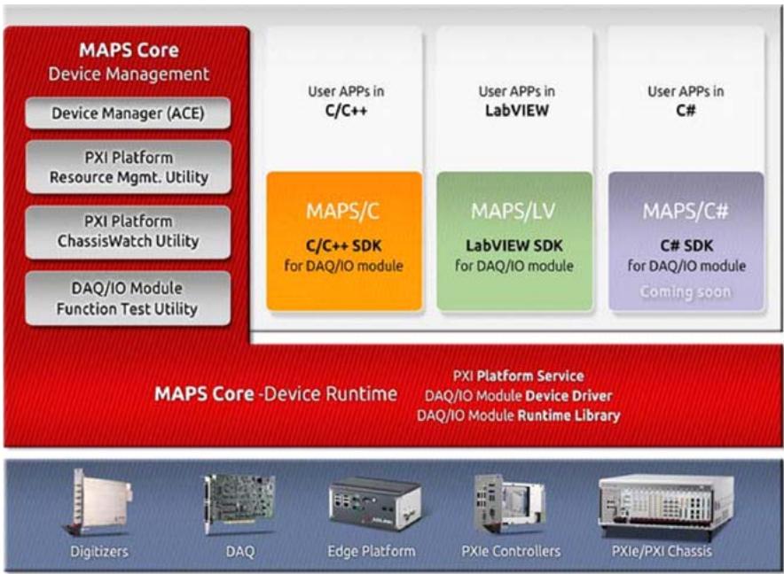
ADLINK provides versatile software drivers and packages to suit various user approaches to building a system. Aside from programming libraries, such as DLLs, for most Windows-based systems, ADLINK also provides drivers for other application environments such as LabVIEW. All software can be downloaded from the ADLINK official website. Commercial software drivers are protected with licensing authorization codes. Without an authorization code, you can install and run the demo version for trial/demonstration purposes for up to two hours. Contact your ADLINK dealer to purchase a software license. ADLINK Measurement, Automation & Platform Service (MAPS) is a software service package designed for data acquisition, automation and PXI platforms.

By leveraging low-level kernel management and a user friendly API, users can easily manage devices under a Windows environment and focus on developing applications.
![This diagram illustrates a layered architecture for a DAQ/IO system. It is organized into four distinct horizontal sections (layers), from top to bottom:\n\n**Top Left Section: Management Utilities**\nThis red vertical column is labeled **'MAPS Core Device Management'** and contains four stacked blocks:\n*   'Device Manager (ACE)'\n*   'PXI Platform Resource Mgmt. Utility'\n*   'PXI Platform ChassisWatch Utility'\n*   'DAQ/IO Module Function Test Utility'\n\n**Top Right Section: User Applications and SDKs**\nThree vertical columns represent different programming environments. Each column has a white block for the application and a colored block for the SDK below it:\n*   **Left Column:** 'User APPs in C/C++' and an orange block labeled 'MAPS/C C/C++ SDK for DAQ/IO module'.\n*   **Middle Column:** 'User APPs in LabVIEW' and a green block labeled 'MAPS/LV LabVIEW SDK for DAQ/IO module'.\n*   **Right Column:** 'User APPs in C#' and a purple block labeled 'MAPS/C# C# SDK for DAQ/IO module Coming soon'.\n\n**Middle Section: Runtime Layer**\nA wide red bar spanning the width of the diagram is labeled **'MAPS Core -Device Runtime'** on the left side. To the right of this label, three items are listed:\n*   'PXI Platform Service'\n*   'DAQ/IO Module Device Driver'\n*   'DAQ/IO Module Runtime Library'\n\n**Bottom Section: Hardware Layer**\nA blue horizontal bar at the bottom displays images of five hardware components, each with a label underneath:\n*   'Digitizers'\n*   'DAQ'\n*   'Edge Platform'\n*   'PXle Controllers'\n*   'PXle/PXI Chassis'](.pci-9112-50m-00070-1000-40/123138de1213220fa7a05a47555dace8b3b28d905d4ffc0e725d567d5dea1fe8.jpg)

# 1.4.1 MAPS Core

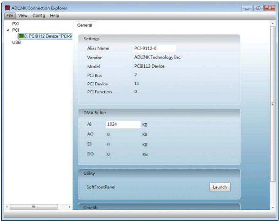
ADLINK MAPS Core is a software package that includes all the device drivers for Windows and a system level management tool called ACE (ADLINK Connection Explorer). With MAPS Core installed, the operating system can identify ADLINK devices and assign the necessary resources for low-level access, such as IO read/write or direct memory access. MAPS Core is necessary for all ADLINK DAQ modules. To ensure the user has the latest software, go to the ADLINK product webpage or contact ADLINK technical service. MAPS Core also comes with a system management portal called ADLINK Connection Explorer (ACE). Through ACE, users can discover and manage ADLINK DAQ modules to reserve a certain size of memory buffer for DMA operation or set the user alias name for operating the module in a LabVIEW environment.
![ADLINK Connection Explorer\nFile View Config Help\nPXI\nPCI\nGeneral\nPCI\n0: PCI9112 Device 'PCI-9'\nUSB\nSettings\nAlias Name PCI-9112-0\nVendor ADLINK Technology Inc.\nModel PCI9112 Device\nPCI Bus 2\nPCI Device 11\nPCI Function 0\nDMA Buffer\nAI 1024 KB\nAO 0 KB\nDI 0 KB\nDO 0 KB\nUtility\nSoftFrontPanel Launch\nCorelib](.pci-9112-50m-00070-1000-40/bdea43e391ffeafb5e64887f6e438330ec5ddc19a2ea7e35a15734ad22b59fb0.jpg)

ADLINK Connection Explorer (ACE) also provides a ready-to-use soft-front panel for digitizer products. Clicking the Launch button in the "Utility" block allows users to control digitizers through the UI and display the acquired waveform/data on the screen.

# 1.4.2 MAPS/LV, LabVIEW Support

Customers who develop their own programs in LabVIEW must install the MAPS/LV software package. MAPS/LV, also called DAQ-LabVIEW Plus, includes the software library and sample program for LabVIEW. For more information, download and install the latest MAPS/LV software from the following website and refer to the MAPS/LV manual:

https://www.adlinktech.com/Products/Data\_Acquisition/DAQSoftware\_Utility/MAPS\_LV

# 1.4.3 MAPS/C, C & C++ Support

Customers who develop their own programs in C or C++ environments must install the MAPS/C software package. MAPS/C includes all the software components required for developing applications in C/C++, such as header files, a device API library and versatile sample programs for understanding how to manipulate the device correctly. Find the latest MAPS/C on the ADLINK website.

https://www.adlinktech.com/Products/Data\_Acquisition/DAQSoftware\_Utility/MAPS\_C

This page intentionally left blank.

# 2 Getting Started

This chapter describes the proper installation environment, installation procedures, package contents and basic information users should be aware of.

![The image displays a white document icon with a folded top-right corner. It features several horizontal gray lines across the page, suggesting text. A large, bold red checkmark is superimposed diagonally over the center of the document.](.pci-9112-50m-00070-1000-40/2ae98c4ef1959b4e92ff19e2b903c9a47bc1b58fc5adb9b8ca3c31f8fd62ed17.jpg)
NOTE:

Diagrams and images of equipment illustrated are for reference only. Actual system configuration and specifications may vary.

# 2.1 Package Contents

Before continuing, check the package contents for any damage and check if the following items are included in the packaging:

▶ PCI-9112 Multifunction DAS Card
PCI-9112 User's Manual

The card contains electro-static sensitive components that can easily be damaged by static electricity. Therefore, the card should be handled on a grounded anti-static mat. The operator should be wearing an anti-static wristband, grounded at the same point as the anti-static mat.

Inspect the card module carton for obvious damage. Shipping and handling may cause damage to your module. Be sure there are no shipping and handling damages on the modules carton before continuing.

After opening the card module carton, extract the system module and place it only on a grounded anti-static surface with component side up.

Inspect the module for any damage. Press down on all the socketed IC's to make sure that they are properly seated. Do this only with the module place on a firm flat surface.

![The image shows a triangular warning sign. It features a red triangle with a white border containing a black exclamation point in the center. Below the triangle, the text 'WARNING!' is written in black capital letters on a white background.](.pci-9112-50m-00070-1000-40/e9bffb2375276100ca0b6b7844277505c7c8e768073054ad0f12e09ec86803b0.jpg)

WARNING: DO NOT install or apply power to equipment that is damaged or if there are missing components. Retain the shipping carton and packing materials for inspection. Please contact your ADLINK dealer/vendor immediately for assistance and obtain authorization before returning any product.

# 2.2 Device Layout and I/O Connectors
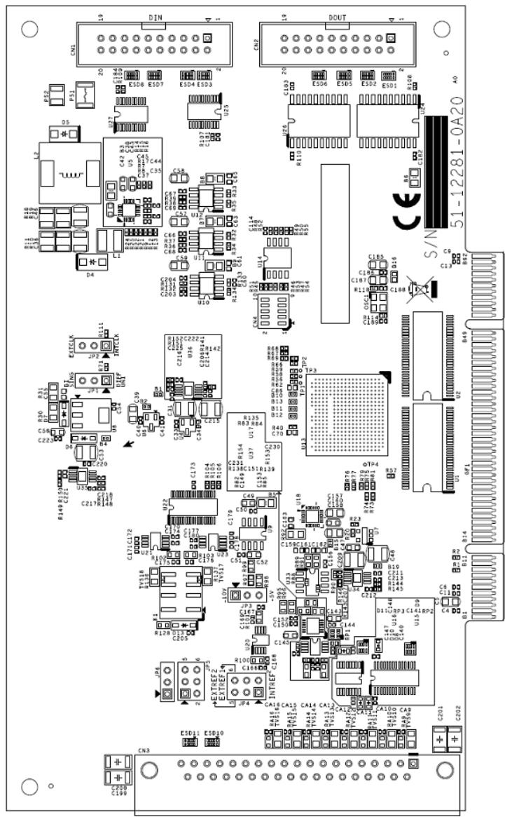
![Circuit board layout diagram with labeled components and connectors, including ICs, resistors, capacitors, and connectors](.pci-9112-50m-00070-1000-40/fe5403843b13471b42d5a24f2648625bb63dea1615534012f5bdb674d8363bfe.jpg)

Figure 2-1: PCB Layout

# 2.3 Jumper Settings

The following items can be configured with jumpers:

▶ analog input signal mode
▶ counter's clock source
▶ analog output range

The card's jumpers and switches are preset at the factory. You can change the jumper settings for your own applications.

<table><tr><td>Configuration</td><td>Attributes</td><td>Jumper</td></tr><tr><td>Analog Inputs</td><td>Single-ended or Differential Analog Input</td><td>JP1</td></tr><tr><td>Clock Source</td><td>Internal Clock or External Clock</td><td>JP2</td></tr><tr><td>D/A Reference Voltage</td><td>-10V or -5V</td><td>JP3</td></tr><tr><td>D/A Reference Source</td><td>Internal Reference or External Reference</td><td>JP4</td></tr></table>

Table 2-1: Jumper Settings

# 2.3.1 Analog Input Channel Configuration

The PCI-9112 offers 16 single-ended or 8 differential analog input channels. Jumper JP1 controls the analog input configurations.

<table><tr><td>Single-ended (default setting)</td><td>&lt;img src="images/cce8e7f38524f3954287d21d3798593926bf3b12f849b479990a7f7568cd691b.jpg"/&gt;</td></tr><tr><td>Differential Input</td><td>&lt;img src="images/7abbe41f671c142b255f1d2127c04d9d91cb132fb17309cbe498d97c7f0c2c04.jpg"/&gt;</td></tr></table>

Table 2-2: Analog Input Channel Configuration

# 2.3.2 Clock Source Settings

A programmable interval timer is used in the PCI-9112. It provides 3 independent 16-bit programmable down counters. The input to counter 2 is connected to a precision 2MHz oscillator for the internal pacer. The input of counter 1 is cascaded from the output of counter 2. Channel 0 is free for user applications. There are two selections for the clock source of channel 0: the internal 2MHz clock or an external clock signal from connector CN3 pin 35.

<table><tr><td>External Clock Source</td><td>&lt;img src="images/66f7227a077c96b8011efc0fcf61be9f64246175462af9c0aebcc73d20f5b512.jpg"/&gt;</td></tr><tr><td>Internal Clock Source: 2MHz (default setting)</td><td>&lt;img src="images/1498a466ad295e8d9aad776bcef35da89c861e9387e940ca2de6757bed06d5f8.jpg"/&gt;</td></tr></table>

Table 2-3: Clock Source Settings

# 2.3.3 D/A Reference Voltage Settings

The D/A converter's reference voltage source can be supplied both internally and externally. The external reference voltage comes from connector CN3, Pin 31 (ExtRef1) and Pin12 (ExtRef2). The reference source of the D/A channel 1 and channel 2 are selected by JP4.

<table><tr><td>D/A CH1 is InternalD/A CH2 is Internal(Default setting)</td><td>ExtRef2JP4 &lt;img src="images/9cc959d89ecb40d9121be7cea6f28a1ceb309492c8e7a270c42858da3302f616.jpg"/&gt;INTREF INTREF</td></tr><tr><td>D/A CH1 is ExternalD/A CH2 is Internal</td><td>ExtRef2JP4 &lt;img src="images/b7664ebf8fbc3609cdf46f46061921fcf27242b621a4be358826747bf7a87c3b.jpg"/&gt;INTREF INTREF</td></tr><tr><td>D/A CH1 is InternalD/A CH2 is External</td><td>ExtRef2JP4 &lt;img src="images/b68ad0f31ba98a3693375f12768d62305500b1499a7230b9a1ff46d79910733b.jpg"/&gt;INTREF INTREF</td></tr><tr><td>D/A CH1 is ExternalD/A CH2 is External</td><td>ExtRef2JP4 &lt;img src="images/1b9b1657689f35ab0fba474877153bca34a7442056d93324652dd7851109ac11.jpg"/&gt;INTREF INTREF</td></tr></table>

Table 2-4: D/A Reference Voltage Settings

The internal D/A reference voltage can be set to -5V or -10V by JP3. The possible configurations are specified in the figure below. Note that the internal reference voltage is used only when the JP4 is set to internal reference only.

<table><tr><td>Reference Voltage is -5V (default setting)</td><td>&lt;img src="images/b897bb358ab5d8e02627905fe86556068b7914bffdf322aaf404f2baf69b91c7.jpg"/&gt; JP3</td></tr><tr><td>Reference Voltage is -10V</td><td>&lt;img src="images/f5a3ba9594ebe8dc5d3fe44404865d79860a5f334b6106d224a695b47194a23c.jpg"/&gt; JP3</td></tr></table>

Table 2-5: Internal Reference Voltage Settings

![The image displays an icon of a white document with a folded top-right corner. Faint grey horizontal lines run across the document. A large, bold red checkmark is superimposed over the center of the document.](.pci-9112-50m-00070-1000-40/9d2ec8c10cbba3c1bded420aa41a52902b8e31aa030d0c4bddf6a2e7d2d2164c.jpg)
NOTE:

If -10V D/A reference voltage is selected, the D/A output range is 0V to 10V. If -5V is selected, the D/A output range is 0V to 5V.

# 2.4 Connector Pin Assignments

The PCI-9112 comes equipped with two 20-pin insulation displacement connectors (CN1 and CN2) and one 37-pin D-type connector (CN3). CN1 and CN2 are located on the board and CN3 is located on the faceplate.

CN1 is for digital signal input, CN2 is for digital signal output, and CN3 is for analog input/output and timer/counter signals.

# 2.4.1 CN3: Analog Input/Output & Counter/Timer

CN3 is a 37-pin D-type connector with the following pin assignments.

(For single-ended connection)
![| Category   | Value |\n| ---------- | ----- |\n| AI0        | 1     |\n| AI1        | 2     |\n| AI2        | 3     |\n| AI3        | 4     |\n| AI4        | 5     |\n| AI5        | 6     |\n| AI6        | 7     |\n| AI7        | 8     |\n| A.GND      | 9     |\n| A.GND      | 10    |\n| V.REF      | 11    |\n| ExtRef2    | 12    |\n| +12V       | 13    |\n| A.GND      | 14    |\n| D.GND      | 15    |\n| COUT0      | 16    |\n| ExtTrg     | 17    |\n| N/C        | 18    |\n| +5V        | 19    |\n| 20         |       |\n| 21         |       |\n| 22         |       |\n| 23         |       |\n| 24         |       |\n| 25         |       |\n| 26         |       |\n| 27         |       |\n| 28         |       |\n| 29         |       |\n| 30         |       |\n| 31         |       |\n| 32         |       |\n| 33         |       |\n| 34         |       |\n| 35         |       |\n| 36         |       |\n| 37         |       |\n| AI8        |       |\n| AI9        |       |\n| AI10       |       |\n| AI11       |       |\n| AI12       |       |\n| AI13       |       |\n| AI14       |       |\n| AI15       |       |\n| A.GND      |       |\n| A.GND      |       |\n| AO1        |       |\n| ExtRef1    |       |\n| AO2        |       |\n| GATE0      |       |\n| GATE1      |       |\n| COUT1      |       |\n| N/C        |       |\nExtCLK    |       |](.pci-9112-50m-00070-1000-40/f57fe3bbac4d7db7ded150aab2e9ccbff75e319f838a8bcefbc5af36927afac7.jpg)

(For differential connection)
![| Category   | Value |\n| ---------- | ----- |\n| AIH0       | 1     |\n| AIH1       | 2     |\n| AIH2       | 3     |\n| AIH3       | 4     |\n| AIH4       | 5     |\n| AIH5       | 6     |\n| AIH6       | 7     |\n| AIH7       | 8     |\n| A.GND      | 9     |\n| A.GND      | 10    |\n| V.REF      | 11    |\n| ExtRef2    | 12    |\n| +12V       | 13    |\n| A.GND      | 14    |\n| D.GND      | 15    |\n| COUT0      | 16    |\n| ExtTrg     | 17    |\n| N/C        | 18    |\n| +5V        | 19    |\n| 20         |       |\n| 21         |       |\n| 22         |       |\n| 23         |       |\n| 24         |       |\n| 25         |       |\n| 26         |       |\n| 27         |       |\n| 28         |       |\n| 29         |       |\n| 30         |       |\n| 31         |       |\n| 32         |       |\n| 33         |       |\n| 34         |       |\n| 35         |       |\n| 36         |       |\n| 37         |       |\n| AIL0       |       |\n| AIL1       |       |\n| AIL2       |       |\n| AIL3       |       |\n| AIL4       |       |\n| AIL5       |       |\n| AIL6       |       |\n| AIL7       |       |\n| A.GND      |       |\n| A.GND      |       |\n| AO1        |       |\n| ExtRef1    |       |\n| AO2        |       |\n| GATE0      |       |\n| GATE1      |       |\n| COUT1      |       |\n| N/C        |       |\nExtCLK    |       |](.pci-9112-50m-00070-1000-40/0a8bed3e282fdf5e224d2dc8aeb002f7394bf2c2056fe9c41b1f7b159f80f6f2.jpg)

Figure 2-2: CN3 Pin Assignments

<table><tr><td>Signal Name</td><td>I/O</td><td>Description</td></tr><tr><td>AI &lt;0...15&gt;</td><td>I</td><td>Signal-ended Analog Input Channels 0-15</td></tr><tr><td>AIH &lt;0...7&gt;</td><td>I</td><td>Differential Analog High Input Channels 0-7</td></tr><tr><td>AIL &lt;0...7&gt;</td><td>I</td><td>Differential Analog Low Input Channels 0-7</td></tr><tr><td>ExtRef &lt;1,2&gt;</td><td></td><td>External Reference Voltage for D/A CH &lt;1,2&gt;</td></tr><tr><td>AO &lt;0,1&gt;</td><td>O</td><td>Analog Output Channels &lt;0,1&gt;</td></tr><tr><td>ExtCLK</td><td>I</td><td>External Clock</td></tr><tr><td>ExtTrig</td><td>I</td><td>External Trigger Signal</td></tr><tr><td>CLK</td><td>I</td><td>Clock Input</td></tr><tr><td>GATE &lt;0,1&gt;</td><td>I</td><td>Gate Input &lt;0,1&gt;</td></tr><tr><td>COUT&lt;0,1&gt;</td><td>O</td><td>Signal Output of Counter Channels &lt;0,1&gt;</td></tr><tr><td>V.ERF</td><td></td><td>Voltage Reference</td></tr><tr><td>A.GND</td><td></td><td>Analog Ground</td></tr><tr><td>D.GND</td><td></td><td>Digital Ground</td></tr></table>

Table 2-6: CN3 Pin Assignment Legend

# 2.4.2 CN1/CN2: Digital Signal Input/Output

CN1 and CN2 are 20-pin insulation displacement connectors for digital signal input/output with the following pin assignments.

![DI 0 —— 1 2 —— DI 1\nDI 2 —— 3 4 —— DI 3\nDI 4 —— 5 6 —— DI 5\nDI 6 —— 7 8 —— DI 7\nDI 8 —— 9 10 —— DI 9\nDI 10 —— 11 12 —— DI 11\nDI 12 —— 13 14 —— DI 13\nDI 14 —— 15 16 —— DI 15\nGND —— 17 18 —— GND\n+5V —— 19 20 —— +12V](.pci-9112-50m-00070-1000-40/de0f706288361e6895de60228a0c34b78901ba710e0adc0940a9b64aab19b841.jpg)

Figure 2-3: CN1 Pin Assignments

![DO 0 —— 1 2 —— DO 1\nDO 2 —— 3 4 —— DO 3\nDO 4 —— 5 6 —— DO 5\nDO 6 —— 7 8 —— DO 7\nDO 8 —— 9 10 —— DO 9\nDO 10 —— 11 12 —— DO 11\nDO 12 —— 13 14 —— DO 13\nDO 14 —— 15 16 —— DO 15\nGND —— 17 18 —— GND\n+5V —— 19 20 —— +12V](.pci-9112-50m-00070-1000-40/3e967811e950fbd3beef5d52ccc1f2071603d2d8f0dbcfcbef7b7d279383eec5.jpg)

Figure 2-4: CN2 Pin Assignments

<table><tr><td>Signal Name</td><td>Description</td></tr><tr><td>DI &lt;0...15&gt;</td><td>Digital Input signal channels 0-15</td></tr><tr><td>DO &lt;0...15&gt;</td><td>Digital Output signal channels 0-15</td></tr><tr><td>GND</td><td>Digital Ground</td></tr></table>

Table 2-7: CN1/CN2 Pin Assignment Legend

# 2.5 Hardware Installation Outline

# 2.5.1 PCI Configuration

PCI cards (or CompactPCI cards) are equipped with plug and play PCI controllers and can request base addresses and interrupts according to PCI standards. The system BIOS will install the system resources based on the PCI cards' configuration registers and system parameters (which are set by the system BIOS). Interrupt assignment and memory usage (I/O port locations) of the PCI cards can only be assigned by system BIOS. These system resource assignments are done on a board-by-board basis. It is not suggested to assign the system resource by any other methods.

# 2.5.2 PCI Slot Selection

A PCI card can be inserted into any PCI slot without any configuration modification to the system resources.

![This is an icon depicting a white document with a folded top-left corner. The document features horizontal lines suggesting text and has a large red checkmark superimposed over it.](.pci-9112-50m-00070-1000-40/61f2d06aeec8026a03d9f18cf900811439a8adc8873e324969a0339fd077fb19.jpg)
NOTE:

The PCI system board and slot must provide bus-mastering capabilities to operate at an optimum level.

# 2.5.3 Installation Procedures

1. Turn off your computer.
2. Turn off all peripherals connected to your computer (printer, monitor, etc.).
3. Remove the cover from your computer.
4. Setup jumpers on the PCI or CompactPCI card.
5. Select a 32-bit PCI slot. PCI slot are shorter than ISA or EISA slots, and are usually white or ivory.
6. Before handling PCI cards, discharge any static buildup on your body by touching the metal case of the computer. Hold the edge and do not touch the components.
7. Position the board into the PCI slot you have selected.
8. Secure the card in place at the rear panel of the system.

# 2.6 Device Installation for Windows Systems

Once Windows 7/10 has started, the Plug and Play function of Windows system will find the new NuDAQ cards. If this is the first time the NuDAQ cards are running on your Windows system, you will be prompted to input the device information source. Please refer to the Software Installation Guide for step-by-step installation procedures.

# 2.7 Daughter Board Connection

The PCI-9112 can be connected with five different daughter boards. The following are compatible: ACLD-8125, 9137, 9138, 9182, 9185, and 9188. The functionality and connections are specified in the following sections.

# 2.7.1 Connect with ACLD-8125

The ACLD-8125 has a 37-pin D-sub connector, which can connect to the PCI-9112 through the 37-pin assemble cable. The most outstanding feature of this daughter board is the onboard CJC (cold junction compensation) circuit. You can directly connect a thermocouple to the ACL-8125 board. The CJC is only suitable for High Gain version boards.

# 2.7.2 Connect with ACLD-9137

The ACLD-9137 is directly connected to cards, which are equipped with 37-pin D-sub connectors. It is suitable for simple applications that do not need complex signaling conditions before an A/D conversion is performed.

# 2.7.3 Connect with ACLD-9182

The ACLD-9182 is a 16-channel isolated digital input board. This board is connected to CN1 of the PCI-9112 via the 20-pin flat cable. The ACLD-9182 provides 500V DC isolation voltage protection, thus protecting your PC system from damage in event that abnormal input signals occur.

![ACLD-9185\nACLD-9182\nCN2\nCN1\nPCI-9112](.pci-9112-50m-00070-1000-40/0fedf799c27daa9b791d87da94e435f8c16dd208195cce12e4ee3ae62b2704eb.jpg)

Figure 2-5: ACLD-9182 Daughter Board Connection

# 2.7.4 Connect with ACLD-9185

The ACLD-9185 is a 16-channel SPDT relay output board. This board is connected to CN2 of the PCI-9112 via a 20-pin flat cable. By using this board, you can control external devices through the digital output signals.

# 2.7.5 Connect with ACLD-9138/ACLD-9188

ACLD-9138 and ACLD-9188 are general-purpose terminal boards equipped with a 37-pin D-sub connector. The ACLD-9138 has an LED indicator to indicate the power ON/OFF status of your computer system.

![Based on the provided image, here is the description of the flowchart/block diagram:\n\n**Labeled Blocks:**\n*   **Left Block:** A large rectangular box containing the text 'CN2' (top left), 'CN1' (middle left), 'CN3' (top right), and 'PCI-9112' (bottom right). On the left side, there are two small vertical grey rectangles. On the right side, there is a connector protruding from the edge.\n*   **Right Block:** A smaller rectangular box containing the text 'ACLD-9188' in the center. Inside the box, there is a horizontal grey bar above the text and another horizontal grey bar below the text.\n\n**Connections:**\n*   A thick black cable connects the connector on the right side of the left block ('PCI-9112') to the left side of the right block ('ACLD-9188'). The cable has connector plugs on both ends.](.pci-9112-50m-00070-1000-40/b54039e268cda5ed8cd9a7adf3892d2818dc5c415c110a5d438c4cc2a8ca7340.jpg)

Figure 2-6: ACLD-9138/9188 Daughter Board Connection

# 3 Operation Theory

This chapter describes the operation theory of the PCI-9112 card functions. The functions include A/D conversion, D/A conversion, Digital I/O and counter/timer usage. The operation theory can help you to understand how to configure or to program the PCI-9112.

# 3.1 A/D Conversion

Before programming the PCI-9112 to perform any A/D conversions, you should have an understanding of the following:

▶ A/D front-end signal input connection
▶ A/D conversion procedure
▶ A/D trigger mode
▶ A/D data transfer mode
▶ Signal Connection

# 3.2 Analog Input Signal Connection

The PCI-9112 provides 16 single-ended or 8 differential analog input channels. The analog signals can be converted to digital values by the A/D converter. To avoid ground loops and to obtain more accurate measurements, it is important to understand the signal source type and how to choose the analog input modes, either signal-ended or differential. The PCI-9112 offers jumpers to select 16 single-ended or 8 different analog inputs.

# Single-ended Mode

The single-ended mode has only one input relative to ground and is suitable for connecting with a floating signal source. A floating source is one that does not have any connection to ground. Figure 3-1 shows the single-ended connection. Note that when more than two floating sources are available, the sources must have a common ground.

![Based on the provided image, here is an accurate and concise description of the flowchart/block diagram:\n\n**Blocks and Text:**\n*   **Floating Signal Source:** On the far left, there are two circles containing sine waves, labeled 'Floating Signal Source'. Below this is the text 'n = 0, ..., 15'.\n*   **Vertical Input Bar:** To the right of the sources is a vertical rectangular bar. The top of the bar is labeled 'AIn' and the bottom is labeled 'AGND'. There are dots along the left edge of this bar representing connection points.\n*   **Input Multiplexer:** A rectangular block in the center is labeled 'Input Multiplexer' below it.\n*   **Operational Amplifier:** To the right of the multiplexer is a triangle symbol labeled 'Operational Amplifier' above it.\n*   **Output:** An arrow extends from the amplifier to the right, labeled below with 'To A/D Converter'.\n*   **Ground:** The bottom of the vertical bar connects to a ground symbol (an inverted triangle).\n\n**Connections:**\n*   Lines connect the 'Floating Signal Source' to the dots on the vertical input bar.\n*   Horizontal lines connect the vertical input bar (labeled 'AIn' and 'AGND') to the 'Input Multiplexer'.\n*   A single line connects the 'Input Multiplexer' to the 'Operational Amplifier'.\n*   The 'Operational Amplifier' outputs to the final destination labeled 'To A/D Converter'.](.pci-9112-50m-00070-1000-40/b2e4d1cabf4dfce450e39a9250d4dca774fe0fed2922f3d2fd2c74d03f93793b.jpg)

Figure 3-1: Floating source and single-ended

# Differential Input Mode

The differential input mode provides two inputs that respond to differences in signals. If the signal source has one side connected to local ground, the differential mode can be used to reduce the effect of ground loops. Figure 3-2 shows the connection for differential input mode. However, if the signal source is locally grounded, the single-ended mode can be used when the Vcm (Common Mode Voltage) is very small and the effect of ground loops is minimal.

![n = 0, ..., 7\nGround\nSignal\nSource\nAlHn\nAlLn\nGND\nTo A/D\nConverter\nVcm = VG1 - VG2\nVG1\nVG2](.pci-9112-50m-00070-1000-40/c2b0e393595959732eed6f42ddc1229499a35a193ae6a967c8de2a92aa5dd227.jpg)

Figure 3-2: Ground source and differential input

A differential mode must be used when the signal source is differential. A differential source means that the ends of the signal are not grounded. To avoid the danger of high voltages between the local ground of the signal and the ground of the PC system, a shorted ground path must be connected. Figure 3-3 shows the connection for a differential source.

![n = 0, ..., 7\nDifferential\nSignal\nSource\nAlHn\nTo A/D\nConverter\nAILn\nGND\nVcm = VG1 - VG2\nVG1\nVG2](.pci-9112-50m-00070-1000-40/844b96aa01f53addf4a8bd7e8dbba1b139b9fd1f916dd3426923dbd8a4da87b8.jpg)

Figure 3-3: Differential source and differential input

If the signal source are both floating, you should use the differential mode, and the floating signal source should be connected as in Figure 3-4.

![**Labeled Blocks:**\n*   **Floating Signal Source**: An AC voltage source symbol on the left.\n*   **Vertical Bar**: A central vertical rectangular bar acting as a bus or switch.\n*   **Triangle**: An amplifier or comparator symbol on the right.\n\n**Connections and Text:**\n*   **Top Path**: The top terminal of the **Floating Signal Source** connects to a wire labeled above with '**n = 0, ..., 7**'. This wire connects to the top of the **Vertical Bar**, near the label '**AlHn**'. From the top of the bar, a wire labeled '**High**' connects to the top input of the **Triangle**.\n*   **Middle Path**: The bottom terminal of the **Floating Signal Source** connects to a wire labeled '**AlLn**' near the **Vertical Bar**. This wire connects to the middle of the bar. From the middle of the bar, a wire labeled '**Low**' connects to the bottom input of the **Triangle**.\n*   **Ground Path**: A wire branches from the **Floating Signal Source**'s bottom terminal (near the '**AlLn**' label) downwards to the bottom of the **Vertical Bar**. From this bottom connection, a wire labeled '**GND**' connects to a ground symbol.\n*   **Output**: The output of the **Triangle** is labeled '**To A/D Converter**'.](.pci-9112-50m-00070-1000-40/4a01dde772665d2ce746c97f7520b56e9f10a31986d32070f087fd86c4a92470.jpg)

Figure 3-4: Floating source and differential input

# 3.2.1 A/D Conversion Procedure

A/D conversion starts when a trigger is set by the trigger source. The PCI-9112 provides three trigger modes. See section 3.2.2.

While A/D conversion is in progress, the DRDY bit in the A/D status register is cleared and indicates that the data is not ready. After the conversion is completed, the DRDY bit will return to active high (1) level. The converted data can now be read from the A/D data registers.

The A/D data should now be transferred into the PC's memory for further processing. The PCI-9112 provides three data transfer modes that allow users to optimize the DAS system. See section 3.2.3 for data transfer modes.

# 3.2.2 A/D Trigger Modes

A/D conversion can be triggered by an Internal or External trigger source. Whenever an external source is set, the internal sources are disabled.

If an internal trigger is selected, either the software trigger or time pacer trigger can be used. The A/D operation mode is controlled by the A/D mode bits of the A/D control register. Totally there are three trigger sources available to the PCI-9112. The different trigger conditions are specified below.

# Software Trigger

This trigger source is software controllable. That is, the A/D conversion starts when any value is written into the software trigger register. This trigger mode is suitable for low speed A/D conversions. Under this mode, the timing of the A/D conversion is fully controlled by the software. However, it is difficult to control a fixed A/D conversion rate unless another timer interrupt service routine is used to generate a fixed rate trigger.

# Timer Pacer Trigger

An FPGA is used as a trigger source for A/D conversion at a fixed rate. Two counters are cascaded together to generate trigger pulses with precise periods (see section 3.5). This mode is ideal for high speed A/D conversion. It can be combined with the DMA bus mastering or the interrupt data transfer. It's recommended that this mode be used if your application needs a fixed and precise A/D sampling rate.

# External Trigger

Through Pin 17 of CN3 (ExtTrig), A/D conversion can also be performed when a rising edge of an external signal is present. The conversion rate of this mode is more flexible than the previous two modes, because the user can control the external signal with the external device. The external trigger can be combined with the DMA transfer, interrupt data transfer, or even program polling data transfer. Generally, the interrupt data transfer is often used when external trigger mode is used.

# 3.2.3 A/D Data Transfer Modes

Any of the three A/D data transfer modes can be used when a conversion is completed. The Data Transfer Mode is controlled by the A/D mode control bits of the A/D control register. The different transfer modes are specified below.

# Software Data Transfer

Usually, this mode is used with software A/D trigger mode. The conversion starts when it receives a software trigger, the software then polls the DRDY bit on the A/D Status register until it becomes high. When it is low, the A/D data is read, and the DRDY bit will be cleared to indicate the data transfer is completed.

It is possible to read A/D converted data without polling. The A/D conversion time takes no more than 2 $\mu$ s on the PCI-9112 card. Hence, after a software trigger, the software can wait for at least 2 $\mu$ s then read the A/D register without polling.

# DMA Transfer

The DMA (Direct Memory Access) bus master allows data to be transferred directly between the PCI-9112 and the PC's memory at the fastest possible rate, without using up any CPU time. The A/D data is queued in the local FIFO on the PCI-9112 itself and it is automatically transferred to PC's memory.

The DMA transfer mode is very complex to program. It is recommended to use high-level programming libraries to operate this card. If you wish to program software to handle the DMA bus master data transfer, refer to the PCI controller manual for more details.

# 3.3 D/A Conversion

D/A conversion is less complex than A/D operation. You only need to write digital values into the D/A data registers and the corresponding voltage will be output to AO1 or AO2. The mathematical relationship between the Digital number DAn and the output voltage is formulated as follows:

$$
V o u t = - V r e f \cdot \frac {D A n}{4 0 9 6}
$$

Where the Vref is the reference voltage, the Vout is the output voltage, and the DAn is the Digital value in the D/A data registers.

Before performing the D/A conversion, users should take care with the D/A reference voltage, which is set by JP3 (see section 2.3 for jumper settings). The reference voltage will affect the output voltage. If the reference voltage is -5V, the D/A output scaling will be 0 to 5V. If the reference voltage is -10V, the D/A output scaling will be 0 to 10V.

The PCI-9112 has two unipolar analog output channels. To make a D/A output connection to the appropriate D/A output, refer to the following diagram.

![Based on the provided block diagram, here is an accurate and concise description:\n\n**Labeled Blocks and Text:**\n*   **Input:** '-5 or -10 INT or Ext' and 'Ref In'\n*   **Component:** A box labeled 'D/A Converter'\n*   **Component:** An operational amplifier (triangle symbol) with inputs labeled '-' and '+'\n*   **Outputs/Connectors:**\n    *   'Pin-30 ( A00 )'\n    *   'Pin-32 ( AO1 )'\n    *   'D/A Output' (with an arrow pointing right)\n    *   'Pin-14 ( A.GND )'\n    *   'Analog GND'\n*   **Ground:** A ground symbol (inverted triangle)\n\n**Connections:**\n1.  **Input to DAC:** The line labeled 'Ref In' connects to the left side of the 'D/A Converter' box.\n2.  **DAC to Op-Amp Input:** A line from the top of the 'D/A Converter' connects to the '-' input of the op-amp.\n3.  **DAC Ground:** A line from the bottom of the 'D/A Converter' connects to the bottom horizontal ground rail.\n4.  **Op-Amp Configuration:**\n    *   The '+' input of the op-amp connects to the bottom horizontal ground rail.\n    *   The output of the op-amp (the tip of the triangle) connects back to the '-' input (feedback loop).\n5.  **Output Bus:**\n    *   The op-amp output connects to the top of a vertical bus bar.\n    *   The bottom of this vertical bus bar connects to the bottom horizontal ground rail.\n6.  **Final Output Labels:**\n    *   From the top of the vertical bus bar, an arrow points right labeled 'D/A Output', accompanied by text 'Pin-30 ( A00 )' and 'Pin-32 ( AO1 )'.\n    *   From the bottom of the vertical bus bar (ground rail), a line extends right labeled 'Pin-14 ( A.GND )' and 'Analog GND'.](.pci-9112-50m-00070-1000-40/31299914609707db23b0957ce7f9e46aab463fb7cbddaa5900935712cd839ecb.jpg)

Figure 3-5: Analog Output Connection

# 3.4 Digital Input and Output

The PCI-9112 provides 16 digital input and 16 digital output channels through the connectors CN1 and CN2 on-board. The digital I/O signal is fully TTL/DTL compatible. The digital I/O signals are illustrated in Figure 3-6.

To program the digital I/O operation is fairly straightforward. The digital input operation is used to read data from corresponding registers, and the digital output operation is to write data to the corresponding registers. Note that the DIO data channel can only be read or written to in groups of 16 bits. It is impossible to access individual bits.

![Digital Input(DI)\nFrom TTL Signal\nDigital Output (DO)\nTo TTL Devices\nDigital GND (DGND)\nPCI-9112\nOutside Device](.pci-9112-50m-00070-1000-40/df7b71e945013aa72b259d9bb4454b8566f2d699f31d2c5e0a5885d66cb9dbc3.jpg)

Figure 3-6: Digital I/O Connection

# 3.5 Timer/Counter Operation

The PCI-9112 has an interval timer/counter onboard. It offers 3 independent 16-bit programmable down counters; counter 1 and counter 2 are cascaded together for the A/D timer pacer trigger of A/D conversions, and counter 0 is free for user applications. Figure 3-7 illustrates the timer/counter connections.

![**Labeled Blocks:**\n*   **Timer/Counter** (The main outer block)\n*   **Counter 0** (Top inner block)\n*   **Counter 1** (Middle inner block)\n*   **Counter 2** (Bottom inner block)\n\n**Connections:**\n*   **CN3 Pin-37** connects to the terminal labeled **EXT**.\n*   **CN3 Pin-33** connects to the middle terminal of the 3-pin header, which also connects to **CLK0**. This middle terminal is connected to **Vcc** via a resistor.\n*   **INT** (the bottom terminal of the 3-pin header) connects to **GATE0**, **GATE1**, and **GATE2**.\n*   **CN3 Pin-34** connects to **CLK1**.\n*   **2MHz Oscillator** connects to **CLK2**.\n*   **OUT0** connects to **CN3 Pin-16**.\n*   **OUT1** connects to **A/D Trigger** and **CN3 Pin-35**.\n*   **OUT2** connects via a feedback loop to the common line feeding **GATE2**.](.pci-9112-50m-00070-1000-40/1350ad8ffdc67d93f8c6762b084a60ac75dd0396b610bacc48f0b3ece275a68c.jpg)

Figure 3-7: Timer/Counter Block Diagram

The clock source of counter 0 can be internal or external, while the gate can be controlled externally and the output is sent to connector CN3. As for counter 1 and counter 2, the clock source is fixed internally, while the gate can be controlled externally and the output is also sent to connector CN3. All timer/counter signals are TTL compatible.

# Pacer Trigger Source

Counters 1 and 2 are cascaded together to generate the timer pacer trigger for A/D conversion. The frequency of the pacer trigger is software controllable. The maximum pacer signal rate is 2MHz/4 = 500KHz which exceeds the maximum A/D conversion rate of the PCI-9112. The minimum signal rate is 2MHz/65535/65535, which is a very slow, and users are advised to not use it.

# General Purpose Timer/ Counter

Counter 0 is free for users applications. The clock source, gate control signal and the output signal are sent to the CN3 connector. The general purpose timer / counter can be used as an event counter, or used for measuring frequency, or others functions.

This page intentionally left blank.

# Important Safety Instructions

For user safety, please read and follow all instructions, Warnings, Cautions, and Notes marked in this manual and on the associated device before handling/operating the device, to avoid injury or damage.

S'il vous plaît prêter attention stricte à tous les avertissements et mises en garde figurant sur l'appareil, pour éviter des blessures ou des dommages.

▶ Read these safety instructions carefully
- Keep the User’s Manual for future reference
▶ Read the Specifications section of this manual for detailed information on the recommended operating environment
▶ The device can be operated at an ambient temperature of $50^{\circ}$ C
- When installing/mounting or uninstalling/removing device; or when removal of a chassis cover is required for user servicing:
▷ Turn off power and unplug any power cords/cables
▷ Reinstall all chassis covers before restoring power

▶ To avoid electrical shock and/or damage to device:

▷ Keep device away from water or liquid sources
▷ Keep device away from high heat or humidity
▷ Keep device properly ventilated (do not block or cover ventilation openings)
▶ Always use recommended voltage and power source settings
▶ Always install and operate device near an easily accessible electrical outlet
▷ Secure the power cord (do not place any object on/over the power cord)
▷ Only install/attach and operate device on stable surfaces and/or recommended mountings

▶ If the device will not be used for long periods of time, turn off and unplug from its power source

▶ Never attempt to repair the device, which should only be serviced by qualified technical personnel using suitable tools

▶ A Lithium-type battery may be provided for uninterrupted backup or emergency power.

![The image displays a standard safety warning sign featuring a yellow equilateral triangle with a thick black border. Inside the triangle is a large black exclamation point. Directly beneath the triangle is a white rectangular box containing the text 'CAUTION:' in black capital letters.](.pci-9112-50m-00070-1000-40/0be7ddc5fb432329297f01a29e6522ae8e67dfc5d2f8b594e3b8012261f3a329.jpg)

Risk of explosion if battery is replaced with one of an incorrect type; please dispose of used batteries appropriately.

Risque d'explosion si la pile est remplacée par une autre de type incorrect. Veuillez jeter les piles usagées de façon appropriée.

▶ The device must be serviced by authorized technicians when:

The power cord or plug is damaged
▷ Liquid has entered the device interior
The device has been exposed to high humidity and/or moisture
The device is not functioning or does not function according to the User's Manual
The device has been dropped and/or damaged and/or shows obvious signs of breakage

▶ Disconnect the power supply cord before loosening the thumbscrews and always fasten the thumbscrews with a screwdriver before starting the system up

It is recommended that the device be installed only in a server room or computer room where access is:

▶ Restricted to qualified service personnel or users familiar with restrictions applied to the location, reasons therefor, and any precautions required
▶ Only afforded by the use of a tool or lock and key, or other means of security, and controlled by the authority responsible for the location

▶ If PoE (Power over Ethernet) is enabled for the device, the system can ONLY be deployed indoors. Unless otherwise noted, the PoE system is NOT designed to withstand the rigors of outdoor use.

![Yellow triangular warning sign with black smoke symbol indicating thermal hazard](.pci-9112-50m-00070-1000-40/76ec3905c44b90a0db5ea3e95700e7d1dcb4f02566d3d1b2a345b7c3096d0478.jpg)

# BURN HAZARD

Touching this surface could result in bodily injury. To reduce risk, allow the surface to cool before touching.

# RISQUE DE BRÛLURES

Ne touchez pas cette surface, cela pourrait entraîner des blessures.

Pour éviter tout danger, laissez la surface refroidir avant de la toucher.

This page intentionally left blank.

# Getting Service

Ask an Expert: http://askanexpert.adlinktech.com

# ADLINK Technology, Inc.

No. 66, Huaya 1st Rd., Guishan District

Taoyuan City 333411, Taiwan

Tel: +886-3-216-5088

Fax: +886-3-328-5706

Email: service@adlinktech.com

# Ampro ADLINK Technology, Inc.

6450 Via Del Oro

San Jose, CA 95119-1208, USA

Tel: +1-408-360-0200

Toll Free: +1-800-966-5200 (USA only)

Fax: +1-408-600-1189

Email: info@adlinktech.com

# ADLINK Technology (China) Co., Ltd.

300 Fang Chun Rd., Zhangjiang Hi-Tech Park

Pudong New Area, Shanghai, 201203 China

Tel: +86-21-5132-8988

Fax: +86-21-5132-3588

Email: market@adlinktech.com

# ADLINK Technology GmbH

Hans-Thoma-Straße 11

D-68163 Mannheim, Germany

Tel: +49-621-43214-0

Fax: +49-621 43214-30

Email: emea@adlinktech.com

Please visit the Contact page at www.adlinktech.com for information on how to contact the ADLINK regional office nearest you:
[🔗 Link to the original document](.pci-9112-50m-00070-1000-40/pci-9112-50m-00070-1000-40.pdf)
