# PCI-9118 DG/L, HG/L, HR/L
PCI-Bus Advanced
Data Acquisition Card
User's Manual
Manual Rev. 3.00
Revision Date: December 28, 2005
Part No: 50-11115-202

Recycled Paper
Copyright 2005 ADLINK TECHNOLOGY INC.
All Rights Reserved.
The information in this document is subject to change without prior notice in order to improve reliability, design, and function and does not represent a commitment on the part of the manufacturer.
In no event will the manufacturer be liable for direct, indirect, special, incidental, or consequential damages arising out of the use or inability to use the product or documentation, even if advised of the possibility of such damages.
This document contains proprietary information protected by copyright. All rights are reserved. No part of this manual may be reproduced by any mechanical, electronic, or other means in any form without prior written permission of the manufacturer.
# Trademarks
Product names mentioned herein are used for identification purposes only and may be trademarks and/or registered trademarks of their respective companies.
# Getting Service from ADLINK
Customer Satisfaction is top priority for ADLINK Technology Inc. Please contact us should you require any service or assistance.
# ADLINK TECHNOLOGY INC.
Web Site: http://www.adlinktech.com
Sales & Service: Service@adlinktech.com
TEL: +886-2-82265877
FAX: +886-2-82265717
Address: 9F, No. 166, Jian Yi Road, Chungho City,
Taipei, 235 Taiwan
Please email or FAX this completed service form for prompt and satisfactory service.
| Company Information |
| Company/Organization | |
| Contact Person | |
| E-mail Address | |
| Address | |
| Country | |
| TEL | FAX: |
| Web Site | |
| Product Information |
| Product Model | |
| Environment | OS:M/B: CPU:Chipset: Bios: |
Please give a detailed description of the problem(s):
# Table of Contents
# Table of Contents...... i
# List of Tables...... x
# List of Figures ...... xi
# 1 Introduction ...... 1
1.1 Features.... 2
1.2 Applications ...... 2
1.3 Specifications.... 3
Analog Input (A/D) 3
Digital I/O (DIO) 4
Programmable Counter 4
General Specifications 4
1.4 Software Support 5
Programming Library 5
DAQ-LVIEW PnP: LabVIEW Driver 5
PCIS-VEE: HP-VEE Driver 6
PCIS-OCX: ActiveX Controls 6
DASYLabTM PRO 6
PCIS-DDE: DDE Server and InTouchTM 6
PCIS-ISG: ISaGRAFTM driver 7
PCIS-ICL: InControlTM Driver 7
PCIS-OPC: OPC Server 7
# 2 Installation 9
2.1 What You Have.... 9
2.2 Unpacking....9
2.3 Device Installation for Windows Systems 10
2.4 PCI-9118DG/L, HG/L Layout 10
2.5 PCI-9118HR/L Layout.... 11
2.6 Hardware Installation Outline.... 11
Hardware configuration 11
PCI slot selection 11
Installation Procedure 12
# 3 Signal Connections.... 13
3.1 Connectors Pin Assignment 13
3.2 Analog Input Signal Connection.... 14
Single-ended Mode 14
Differential input mode 15
3.3 Digital I/O Connection 16
3.4 Timer / Counter Connection.... 17
# 4 Registers Format 19
4.1 I/O Port Address 19
4.2 A/D Data Registers 20
4.3 A/D control Register 21
4.4 A/D Status Register 23
4.5 Digital I/O register 25
4.6 Software Trigger Register 26
4.7 Internal Timer/Counter Register 26
4.8 A/D Gain/Channel Register 27
4.9 A/D Burst Number Register 27
4.10 A/D Auto Scan Mode 28
4.11 A/D Function Register 29
4.12 A/D FIFO Reset Register 31
4.13 Interrupt Control Register 32
4.14 Interrupt Status Register 33
# 5 Operation Theorem...... 35
5.1 A/D Conversion.... 35
A/D Conversion Procedure 35
A/D Trigger Sources and conversion modes 35
A/D Data Transfer Modes 38
Trigger Acquisition Modes 39
Specifying Channels and Gains in the Channel-Gain Queue 41
5.2 Digital Input and Output 41
5.3 Timer/Counter Operation 41
# 6 C/C++ Library 47
6.1 Libraries Installation 47
6.2 Programming Guide.... 48
Naming Convention 48
Data Types 48
6.3 \_9118\_Initial 49
@ Description 49
@ Syntax 49
@ Argument 49 @ Return Code 50
6.4 \_9118\_Switch\_Card\_No.... 51
@ Description 51
@ Syntax 51
@ Argument 51
@ Return Code 51
6.5 \_9118\_DI 52
@ Description 52
@ Syntax 52
@ Argument 52
@ Return Code 52
6.6 \_9118\_DI\_Channel.... 53
@ Description 53
@ Syntax 53
@ Argument 53
@ Return Code 53
6.7 \_9118\_DO 54
@ Description 54
@ Syntax 54
@ Argument 54
@ Return Code 54
6.8 \_9118\_AD\_Reset\_AFIFO 55
@ Description 55
@ Syntax 55
@ Argument 55
@ Return Code 55
6.9 \_9118\_AD\_Bgnset\_AFIFO 56
@ Description 56
@ Syntax 56
@ Argument 56
@ Return Code 56
6.10 \_9118\_AD\_Endset\_AFIFO 57
@ Description 57
@ Syntax 57
@ Argument 57
@ Return Code 57
6.11 \_9118\_AD\_Reset\_DFIFO.... 58
@ Description 58
@ Syntax 58
@ Argument 58
@ Return Code 58
6.12 \_9118\_AD\_Set\_Burst\_No.... 59
@ Description 59
@ Syntax 59
@ Argument 59
@ Return Code 59
6.13 \_9118\_INT\_Set\_CtrlReg.... 60
@ Description 60
@ Syntax 60
@ Argument 60
@ Return Code 60
6.14 \_9118\_AD\_Set\_GainChn 61
@ Description 61
@ Syntax 61
@ Argument 61
@ Return Code 62
6.15 \_9118\_AD\_Set\_Scan 63
@ Description 63
@ Syntax 63
@ Argument 63
@ Return Code 63
6.16 \_9118\_AD\_Soft\_Trig 65
@ Description 65
@ Syntax 65
@ Argument 65
@ Return Code 65
6.17 \_9118\_AD\_Set\_Unip 66
@ Description 66
@ Syntax 66
@ Argument 66
@ Return Code 66
6.18 \_9118\_AD\_Set\_Diff 67
@ Description 67
@ Syntax 67
@ Argument 67
@ Return Code 67
6.19 \_9118\_AD\_Set\_SoftG 68
@ Description 68
@ Syntax 68
@ Argument 68
@ Return Code 68
6.20 9118 AD Set ExtG 69
@ Description 69
@ Syntax 69
@ Argument 69
@ Return Code 69
6.21 9118 AD Set ExtM 70
@ Description 70
@ Syntax 70
@ Argument 70
@ Return Code 70
6.22 9118 AD Set TmrTr.... 71
@ Description 71
@ Syntax 71
@ Argument 71
@ Return Code 71
6.23 9118 AD Set Int 72
@ Description 72
@ Syntax 72
@ Argument 72
@ Return Code 72
6.24 \_9118\_AD\_Set\_Dma.... 73
@ Description 73
@ Syntax 73
@ Argument 73
@ Return Code 73
6.25 \_9118\_AD\_Set\_CtrlReg 74
@ Description 74
@ Syntax 74
@ Argument 74
@ Return Code 74
6.26 \_9118\_AD\_Set\_PDTrg 75
@ Description 75
@ Syntax 75
@ Argument 75
@ Return Code 75
6.27 \_9118\_AD\_Set\_PETrg 76
@ Description 76
@ Syntax 76
@ Argument 76
@ Return Code 76
6.28 \_9118\_AD\_Set\_BSSH.... 77
@ Description 77
@ Syntax 77
@ Argument 77
@ Return Code 77
6.29 \_9118\_AD\_Set\_BM 78
@ Description 78
@ Syntax 78
@ Argument 78
@ Return Code 78
6.30 \_9118\_AD\_Set\_BS.... 79
@ Description 79
@ Syntax 79
@ Argument 79
@ Return Code 79
6.31 \_9118\_AD\_Set\_PM 80
@ Description 80
@ Syntax 80
@ Argument 80
@ Return Code 80
6.32 \_9118\_AD\_Set\_AM 81
@ Description 81
@ Syntax 81
@ Argument 81
@ Return Code 81
6.33 \_9118\_AD\_Set\_Start 82
@ Description 82
@ Syntax 82
@ Argument 82
@ Return Code 82
6.34 \_9118\_AD\_Set\_FuncVal 83
@ Description 83
@ Syntax 83
@ Argument 83
@ Return Code 83
6.35 \_9118\_AD\_Aquire.... 84
@ Description 84
@ Syntax 84
@ Argument 84
@ Return Code 84
6.36 \_9118\_AD\_DMA\_Start 85
@ Description 85
@ Syntax 85
@ Argument 85
@ Return Code 87
6.37 \_9118\_AD\_DMA\_Status.... 88
@ Description 88
@ Syntax 88
@ Argument 88
@ Return Code 88
6.38 \_9118\_AD\_DMA\_Stop 89
@ Description 89
@ Syntax 89
@ Argument 89
@ Return Code 89
6.39 \_9118\_ContDmaStart 90
@ Description 90
@ Syntax 90
@ Argument 91
@ Return Code 92
6.40 \_9118\_CheckHalfReady.... 93
@ Description 93
@ Syntax 93
@ Argument 93
@ Return Code 93
6.41 \_9118\_DblBufferTransfer 94
@ Description 94
@ Syntax 94
@ Argument 94
@ Return Code 94
6.42 \_9118\_GetOverrunStatus.... 95
@ Description 95
@ Syntax 95
@ Argument 95
@ Return Code 95
6.43 \_9118\_ContDmaStop 96
@ Description 96
@ Syntax 96
@ Argument 96
@ Return Code 96
6.44 9118 AD INT Start.... 97
@ Description 97
@ Syntax 97
@ Argument 97
@ Return Code 98
6.45 \_9118\_AD\_INT\_Status 99
@ Description 99
@ Syntax 99
@ Argument 99
@ Return Code 99
6.46 \_9118\_AD\_INT\_Stop.... 100
@ Description 100
@ Syntax 100
@ Argument 100
@ Return Code 100
6.47 \_9118\_TIMER\_Start 101
@ Description 101
@ Syntax 101
@ Argument 101
@ Return Code 101
6.48 \_9118\_TIMER\_Read 102
@ Description 102
@ Syntax 102
@ Argument 102
@ Return Code 102
6.49 \_9118\_TIMER\_Stop 103
@ Description 103
@ Syntax 103
@ Argument 103
@ Return Code 103
6.50 W\_9118\_Set\_Trig 104
@ Description 104
@ Syntax 104
@ Argument 104
@ Return Code 105
6.51 W\_9118\_Alloc\_AI\_Mem 106
@ Description 106
@ Syntax 106
@ Argument 106
@ Return Code 106
6.52 W 9118 Free AI Mem.... 107
@ Description 107
@ Syntax 107
@ Argument 107
@ Return Code 107
6.53 W\_9118\_Get\_Sample 108
@ Description 108
@ Syntax 108
@ Argument 108
@ Return Code 108
# 7 Calibration.... 109
7.1 What do you need.... 109
7.2 VR Assignment 109
7.3 A/D Adjustment.... 110
Bipolar Calibration 110
Unipolar Calibration 110
# 8 Software Utility 111
8.1 Running 9118util.exe 111
8.2 System Configuration 112
8.3 Calibration.... 113
8.4 Functional Testing 115
# Warranty Policy.... 117
# List of Tables
Table 4-1: I/O Address 19
Table 7-1: VRs Functions 109
# List of Figures
Figure 2-1: PCB Layout of the PCI-9118DG/L, HG/L 10
Figure 2-2: PCB Layout of the PCI-9118HR/L 11
Figure 3-1: Pin Assignment of CN1 13
Figure 3-2: Floating source and single-ended 15
Figure 3-3: Ground-referenced source and differential input ..... 15
Figure 3-4: Floating source and differential input.... 16
Figure 3-5: Digital I/O Connection.... 16
Figure 3-6: Block Diagram of 8254 Timer/Counter 17
Figure 8-1: Function Testing Menu Window 115
Figure 8-2: A/D with Polling Test window 116
# 1 Introduction
The PCI-9118/L series are the simplified version of the phase-out PCI-9118 series. The PCI-9118/L series provides fully compatible functionalities as the PCI-9118 series except the analog output function. The PCI-9118DG/L and PCI-9118HG/L feature 12-bit resolution, with sampling rate up to 333kS/s, and the PCI-9118HR/L features 16-bit resolution, with sampling rate up to 100kS/s. The 256-location channel-gain queues on PCI-9118/L series allow high-speed data acquisition with different gains on each channel and non-sequential order of automatic analog input scanning capability. The on-board 1k-sample A/D FIFO ensures reliable high-speed data acquisition under Windows operating system. The data can be transferred through bus-mastering DMA with gap-free, continuous high throughput, even for a large amount of data.
# 1.1 Features
The PCI-9118/L PCI Bus Advanced Data Acquisition Card provides the following advanced features:
▶ 32-bit PCI-Bus, plug and play
▶ 12-bit (9118DG/L, HG/L) or 16-bit (9118HR/L) analog input resolution
▶ On-board A/D 1K FIFO memory
▶ Channel-Gain queue for high speed acquisition at different gain
▶ Up to 330KHz (9118DG/L, HG/L) or 100KHz (9118HR/L) A/D sampling rate Bipolar or Unipolar input signals
▶ Auto-scanning channel selection
▶ 16 single-ended or 8 differential analog input channels
▶ Bipolar or Unipolar input signals
▶ Programmable gain of x1, x2, x4, x8 (9118DG/L, HR/L) or x1, x10, x100, x1000 (9118HG/L)
▶ Programmable burst mode sampling emulates simultaneous sample & hold
▶ 4 digital input and 4 digital output channels
▶ Three A/D trigger modes : software trigger, programmable pacer trigger, and external pulse trigger.
▶ 50-pin D-type connector
▶ Compact size : half-size PCB
# 1.2 Applications
▶ Industrial and laboratory ON/OFF control
▶ Energy management
▶ Annunciation
▶ 16 TTL/DTL compatible digital input channels
▶ Security controller
▶ Product test
▶ BCD interface driver
# 1.3 Specifications
# Analog Input (A/D)
▶ Converter:
9118DG/L, HG/L: B.B. ADS7800 or equivalent
▷ 9118HR/L: B.B. ADS7805 or equivalent
▶ Input Channels: 16 single-ended or 8 differential
▶ A/D FIFO Buffer Size: 1024 location
▶ Channel/Gain Queue Length: 256 location
▶ Resolution: 12-bit (9118DG/L, HG/L) or 16-bit(9118HR/L)
▶ Input Range: (Software controlled)
▷ 9118DG/L, HR/L:
Bipolar: ±5V, ±0.5V, ±0.25V, ±0.625V
Unipolar: 0\~10V, 0\~5V, 0\~2.5V, 0\~1.25V
9118HG/L:
Bipolar: ±5V, ±0.5V, ±0.05V, ±0.005V
Unipolar: 0\~10V, 0\~1V, 0\~0.1V, 0\~0.01V
▶ Overvoltage Protection: 70V peak-to-peak
▶ On chip sample-and hold
▶ Accuracy:
▷ 0.01% of FSR ±1 LSB
▷ 0.02% of FSR ±1 LSB
▶ Input Impedance: 10,000 MΩ // 6pF
▶ Trigger Mode: Pre-trigger, Post-trigger, and About-Trigger
▶ Data Transfer: Program control, Interrupt, DMA (Bus mastering)
▶ Data Throughput:
▷ 330KHz (maximum) for 9118DG/L, HG/L
▷ 100KHz (maximum) for 9118HR/L
# Digital I/O (DIO)
▶ Channel: 4 TTL compatible inputs and outputs
▶ Input Voltage:
▷ Low: VIL=0.8 V max.; IIL=0.2mA max.
▷ High: VIH=2.0V max.; IIH=0.02mA max
▶ Output Voltage :
▷ Low: VOL=0.5 V max.; IOL=8mA max.
▷ High: VOH=2.7V min; IOH=400μA
# Programmable Counter
▶ Device: 82C54
▶ A/D Pacer: 32-bit timer (two 16-bit counter cascaded together) with a 4MHz time base
▶ Max Pacer Rate: 333 KHz
▶ Min Pacer Rate: 0.0012 Hz
# General Specifications
▶ Connector: 50-pin D-type SCSI-II connector
▶ Operating Temperature: 0°C \~ 60°C
▶ Storage Temperature: $-20^{\circ}C \sim 80^{\circ}C$
▶ Humidity: 5 \~ 95%, non-condensing
▶ Power Consumption:
PCI-9118DG/L, HG/L
+5V@450mA typical
+12V@200mA typical
-12V@50mA typical
PCI-9118HR/L
+5V@485mA typical
+12V@180mA typical
-12V@50mA typical
▶ Dimension: Compact size only 102mm (H) x 173mm (L)
# 1.4 Software Support
ADLINK provides versatile software drivers and packages for users' different approach to built-up a system. We not only provide programming library such as DLL for many Windows systems, but also provide drivers for many software package such as LabVIEWR, HP VEETM, DASYLabTM, InTouchTM, InControlTM, ISaGRAFTM, etc.
All the software options are included in the ADLINK CD. The non-free software drivers are protected with serial licensed code. Without the software serial number, you can still install them and run the demo version for two hours for demonstration purpose. Please contact with your dealer to purchase the formal license serial code.
# Programming Library
For customers who are writing their own programs, we provide function libraries for many different operating systems, including:
▶ DOS Library: Borland C/C++ and Microsoft C++, the functions descriptions are included in this user's guide.
Windows 95 DLL: For VB, VC++, Delphi, BC5, the functions descriptions are included in this user's guide.
PCIS-DASK: Include device drivers and DLL for Windows 98/NT/2000/XP. DLL is binary compatible across Windows 98/NT/2000/XP. That means all applications developed with PCIS-DASK are compatible across Windows 98/NT/2000/XP. The developing environment can be VB, VC++, Delphi, BC5, or any Windows programming language that allows calls to a DLL. The user's guide and function reference manual of PCIS-DASK are in the CD. Please refer the PDF manual files under \\Manual\Software Package\PCIS-DASK The above software drivers are shipped with the board. Please refer to the "Software Installation Guide" to install these drivers.
# DAQ-LVIEW PnP: LabVIEW Driver
DAQ-LVIEW PnP contains the VIs, which are used to interface with NI's LabVIEW® software package. The DAQ-LVIEW PnP supports Windows 98/NT/2000/XP. The LabVIEW® drivers are free shipped with the board. You can install and use them without license. For detail information about DAQ-LVIEW PnP, please refer to the user's guide in the CD.(\\ Manual\Software Package\DAQ-LVIEW PnP)
# PCIS-VEE: HP-VEE Driver
The PCIS-VEE includes the user objects, which are used to interface with HP VEE software package. PCIS-VEE supports Windows 95/98/NT. The HP-VEE drivers are free shipped with the board. You can install and use them without license. For detail information about PCIS-VEE, please refer to the user's guide in the CD.
(\Manual\Software Package\PCIS-VEE)
# PCIS-OCX: ActiveX Controls
We suggest the customers who are familiar with ActiveX controls and VB/VC++ programming use the PCIS-OCX ActiveX Control components library for developing applications. The PCIS-OCX is designed under Windows NT/98/2000/XP. For more detailed information about PCIS-OCX, please refer to the user's guide in the CD.
(\Manual\Software Package\PCIS-OCX)
# DASYLabTM PRO
DASYLab is an easy-to-use software package, which provides easy-setup instrument functions such as FFT analysis. Please contact us to get DASYLab PRO, which include DASYLab and ADLINK hardware drivers.
# PCIS-DDE: DDE Server and InTouchTM
DDE stands for Dynamic Data Exchange specifications. The PCIS-DDE includes the PCI cards' DDE server. The PCIS-DDE server is included in the ADLINK CD. It needs license. The DDE server can be used conjunction with any DDE client under Windows NT.
# PCIS-ISG: ISaGRAFTM driver
The ISaGRAF WorkBench is an IEC1131-3 SoftPLC control program development environment. The PCIS-ISG includes ADLINK products target drivers for ISaGRAF under Windows NT environment. The PCIS-ISG is included in the ADLINK CD. It needs license.
# PCIS-ICL: InControlTM Driver
PCIS-ICL is the InControl driver which support the Windows NT. The PCIS-ICL is included in the ADLINK CD. It needs license.
# PCIS-OPC: OPC Server
PCIS-OPC is an OPC Server, which can link with the OPC clients. There are many software packages on the market can provide the OPC clients now. The PCIS-OPC supports the Windows NT. It needs license.
# 2 Installation
This chapter describes how to install the PCI-9118DG/L, HG/L, HR/L. The contents in the package and unpacking information that you should be careful are described.
The PCI-9118DG/L, HG/L, HR/L supports plug-and-play and the IRQ, port address and BIOS address are assigned automatically. So, you do not need to set above configuration as you use ISA form factor DAS card. For system reliability, some critical settings for analog input and output need to be assigned manually, because these settings will not be changed after your data acquisition system configuration is decided. It will let your system get more reliability and safety (users can not change the configuration by software directly) when your system is running.
# 2.1 What You Have
In addition to this User's Guide, the package includes the following items:
PCI-9118/L Enhanced Multi-function Data Acquisition Card
▶ ADLINK CD
▶ Software Installation Guide
If any of these items is missing or damaged, contact the dealer from whom you purchased the product. Save the shipping materials and carton in case you want to ship or store the product in the future.
# 2.2 Unpacking
Your PCI-9118/L card contains sensitive electronic components that can be easily damaged by static electricity.
The card should be handled on a grounded anti-static mat. The operator should be wearing an anti-static wristband, grounded at the same point as the anti-static mat.
Inspect the card module carton for obvious damage. Shipping and handling may cause damage to your module. Be sure there are no shipping and handing damages on the module before processing.
After opening the card module carton, extract the system module and place it only on a grounded anti-static surface with component side up.
Again inspect the module for damage. Press down on all the socketed IC's to make sure that they are properly seated. Do this only with the module place on a firm flat surface.
Note : DO NOT APPLY POWER TO THE CARD IF IT HAS BEEN DAMAGED.
You are now ready to install your PCI-9118/L.
# 2.3 Device Installation for Windows Systems
Once Windows 98/NT/2000/XP has started, the Plug and Play function of Windows system will find the new NuDAQ/NuIPC cards. If this is the first time to install NuDAQ/NuIPC cards in your Windows system, you will be informed to input the device information source. Please refer to the "Software Installation Guide" for the steps of installing the device.
# 2.4 PCI-9118DG/L, HG/L Layout
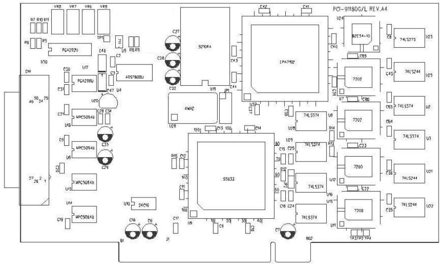
Figure 2-1: PCB Layout of the PCI-9118DG/L, HG/L
# 2.5 PCI-9118HR/L Layout
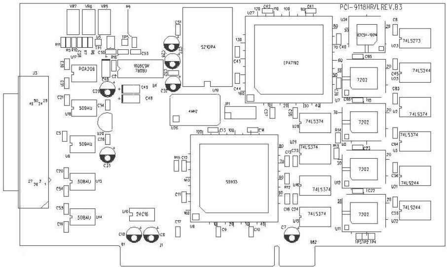
Figure 2-2: PCB Layout of the PCI-9118HR/L
# 2.6 Hardware Installation Outline
# Hardware configuration
The PCI cards (or CompactPCI cards) are equipped with plug and play PCI controller, it can request base addresses and interrupt according to PCI standard. The system BIOS will install the system resource based on the PCI cards' configuration registers and system parameters (which are set by system BIOS). Interrupt assignment and memory usage (I/O port locations) of the PCI cards can be assigned by system BIOS only. These system resource assignments are done on a board-by-board basis. It is not suggested to assign the system resource by any other methods.
# PCI slot selection
The PCI card can be inserted to any PCI slot without any configuration for system resource.
# Installation Procedure
1. Turn off your computer.
2. Turn off all accessories (printer, modem, monitor, etc.) connected to your computer.
3. Remove the cover from your computer.
4. Setup jumpers on the PCI or CompactPCI card.
5. Select a 32-bit PCI slot. PCI slot are short than ISA or EISA slots, and are usually white or ivory.
6. Before handling the PCI cards, discharge any static buildup on your body by touching the metal case of the computer. Hold the edge and do not touch the components.
7. Position the board into the PCI slot you selected.
8. Secure the card in place at the rear panel of the system.
# 3 Signal Connections
This chapter describes the connector of the PCI-9118/L, also the signal connection between the PCI-9118/L and external devices, such as daughter boards or other devices.
# 3.1 Connectors Pin Assignment
The PCI-9118/L is equipped one 50-pin D-type connector - CN1.
CN1 for digital signal input, digital signal output, analog input, analog output and timer/counter's signals. The pin assignment for each connectors are illustrated in Figure 3.1.
CN1 - Digital Signal Input, Digital Signal Output, Analog Input/Output & Counter/Timer
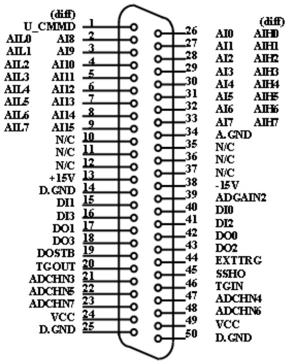
Figure 3-1: Pin Assignment of CN1
# Legend:
▶ U\_CMMD: User Defines Command Mode
▶ Aln: Analog Input Channel n (single-ended)
▶ AIHn: Analog High Input Channel n (differential)
▶ AILn: Analog Low Input Channel n (differential)
▶ EXTTRG: External Trigger Signal or External CLK
▶ DIn: Digital Input Signal Channel n
▶ DOn: Digital Output Signal Channel n
▶ TGIN: Exernal Digital Trigger or Hardware Gate
▶ TGOUT: Trigger/Gate Output Signal
▶ SSHO: SSH Output Signal
▶ DOSTB: Strobe Signal
▶ ADCHNn: Multiplexer Control Line n
▶ ADGAIN2: External Gain Control Line
▶ A.GND: Analog Ground
▶ D.GND: Digital Ground
# 3.2 Analog Input Signal Connection
The PCI-9118/L provides 16 single-ended or 8 differential analog input channels. The analog signal can be converted to digital value by the A/D converter. To avoid ground loops and get more accuracy measurement of A/D conversion, it is quite important to understand the signal source type and how to choose the analog input modes: signal-ended and differential. The PCI-9118/L offers jumpers to select 16 single-ended or 8 different analog inputs.
# Single-ended Mode
The single-ended mode has only one input relative to ground and it suitable for connecting with the floating signal source. The floating source means it does not have any connection to ground. Figure 3.2 shows the single-ended connection. Note that when more than two floating sources are connected, the sources must be with common ground.
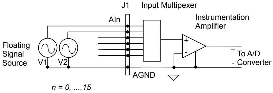
Figure 3-2: Floating source and single-ended
# Differential input mode
The differential input mode provides two inputs that respond to the difference signal between them. If the signal source has one side connected to local ground, the differential mode can be used for reducing ground loop. Figure 3.3 shows the connection of the differential input mode. However, even if the signal source is local grounded, the single-ended still can be used when the Vcm (Common Mode Voltage) is very small and the effect of ground loop can be negated.
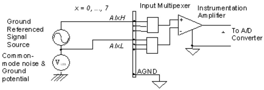
Figure 3-3: Ground-referenced source and differential input
If your signal source is both floating and local ground, you should use the differential mode, and the floating signal source should be connected as the Figure 3.4.
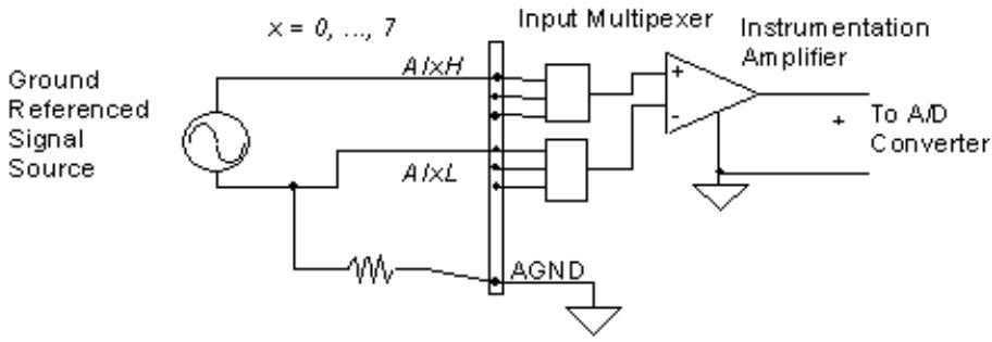
Figure 3-4: Floating source and differential input
# 3.3 Digital I/O Connection
The PCI-9118/L provides 4 digital input and 4 digital output channels on board. The digital I/O signal are fully TTL/DTL compatible. The detailed digital I/O signal specification can be referred in section 1.3.
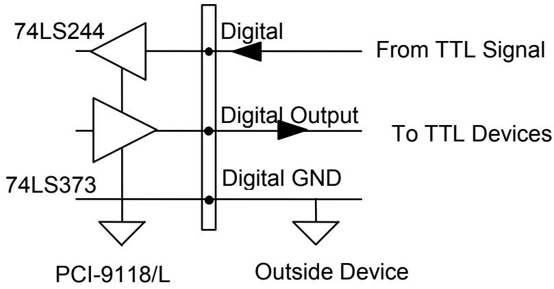
Figure 3-5: Digital I/O Connection
# 3.4 Timer / Counter Connection
The PCI-9118/L has an internal timer/counter 8254 on board. It offers 3 independent 16-bit programmable down counters; counter 1 and counter 2 are cascaded together for A/D timer pacer trigger of A/D conversion, and counter 0 is used as post counter by about-trigger mode and post-trigger mode. Figure 3.6 shows the 8254 timer/counter connection.
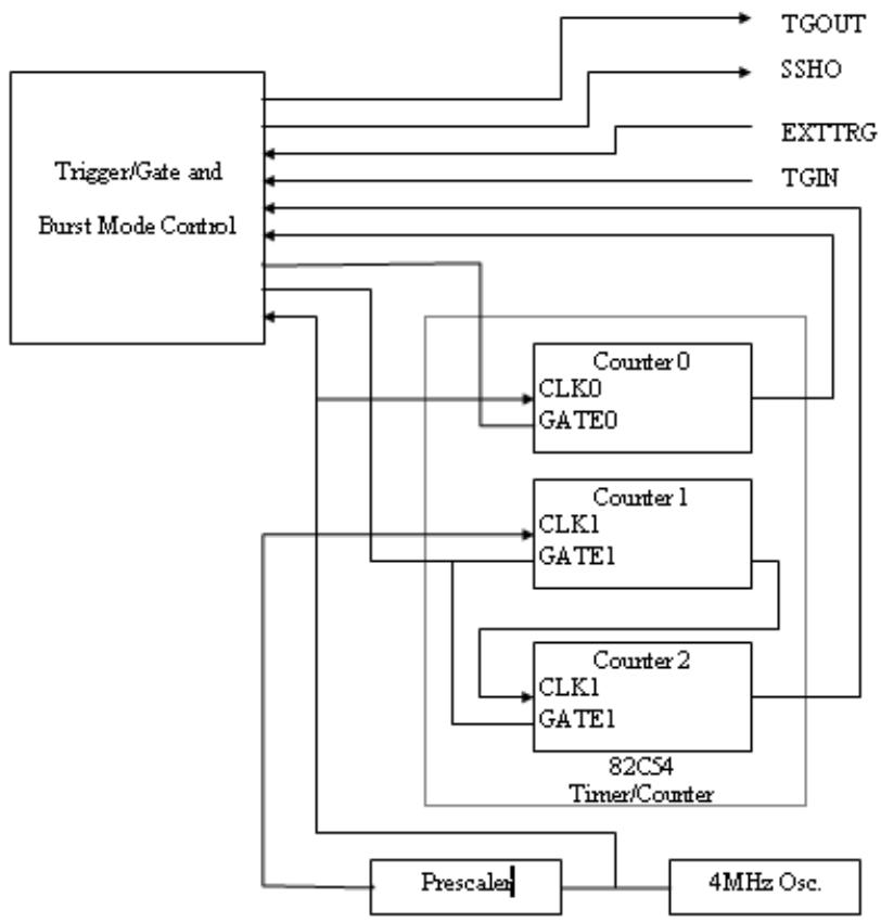
Figure 3-6: Block Diagram of 8254 Timer/Counter
The clock source of A/D conversion can be internal or external from EXTTRIG (pin44). The clock sources of counter1 and counter2 are internally fixed, while the gate can be controlled externally by TRIN (pin46). All the timer/ counter signals are TTL compatible.
# 4 Registers Format
The detailed descriptions of the register format and structure of the PCI-9118DG/L, HG/L, HR/L are specified in this chapter. This information is quite useful for the programmer, who wishes to handle the card by low-level program.
In addition, the low level programming syntax is introduced. This information can help the beginners to operate the PCI-9118DG/L, HG/L, HR/L in the shortest learning time.
# 4.1 I/O Port Address
The PCI-9118DG/L, HG/L, HR/L functions as 32-bit PCI target device to any master on the PCI bus. It supports burst transfer to memory space by using 32-bit data. So, all data read and write will base on 32-bit data. The Table 4.1 shows the I/O address of each register with respect to the base address. The function of each register also be shown.
| I/O Address | Read | Write |
| Base + 0x00 | Counter 0 | Counter 0 |
| Base + 0x04 | Counter 1 | Counter 1 |
| Base + 0x08 | Counter 2 | Counter 2 |
| Base + 0x0C | ---- | 8254 Counter Control |
| Base + 0x10 | A/D Data Reg. | ---- |
| Base + 0x14 | ---- | ---- |
| Base + 0x18 | A/D Status Reg. | A/D Control Reg. |
| Base + 0x1C | Digital IN Reg. | Digital OUT Reg. |
| Base + 0x20 | ---- | Software Trigger |
| Base + 0x24 | ---- | A/D Gain/Channel Reg. |
| Base + 0x28 | ---- | A/D Burst No. Reg. |
| Base + 0x2C | ---- | A/D Auto Scan Mode |
| Base + 0x30 | ---- | A/D Function Reg. |
| Base + 0x34 | ---- | A/D Data FIFO Reset |
| Base + 0x38 | Interrupt Reason Reg. | Interrupt Control Reg. |
Table 4-1: I/O Address
# 4.2 A/D Data Registers
The PCI-9118/L provides 16 single-ended or 8 differential A/D input channels, the digital data will store in the A/D data registers. The 12 bits A/D data is put into 32 bits registers.
▶ Address: BASE + 10
▶ Attribute: read only
▶ Data Format:
| Bit | 7 | 6 | 5 | 4 | 3 | 2 | 1 | 0 |
| BASE+10 | AD3 | AD2 | AD1 | AD0 | CH3 | CH2 | CH1 | CH0 |
| BASE+11 | AD11 | AD10 | AD9 | AD8 | AD7 | AD6 | AD5 | AD4 |
| BASE+12 | --- | --- | --- | --- | --- | --- | --- | --- |
| BASE+13 | --- | --- | --- | --- | --- | --- | --- | --- |
AD11 .. AD0 : Analog to digital data. AD11 is the Most Significant Bit (MSB).AD0 is the Least Significant Bit (LSB).
▷ CH3 \~ CH0 : A/D channel number from which the data is derived.
▷ --- : Don't care
# 4.3 A/D control Register
This register is used to control the A/D mode. It's a write only register.
▶ Address: BASE + 18
▶ Attribute: write only
▶ Data Format:
| Bit | 7 | 6 | 5 | 4 | 3 | 2 | 1 | 0 |
| Base + 18 | UniP | Diff | SoftG | ExtG | ExtM | TmrTr | Int | Dma |
| Base + 19 | --- | --- | --- | | | | | |
| Base + 1A | --- | --- | --- | --- | --- | --- | --- | --- |
| Base + 1B | --- | --- | --- | --- | --- | --- | --- | --- |
▷ UniP (Bit7) : Unipolar or Bipolar A/D input
1: unipolar
0: bipolar
▷ Diff (Bit6) : Differential or Single ended A/D input
1: Differential End
0: Single End
▷ SoftG(Bit5):Software Gate Control Output
1: 8254 counter works
0: 8254 counter stops
▷ ExtG(Bit4):External or Soft Gate Control Mode
1: 8254 counter controlled by TGIN(connector pin 46)
0: 8254 counter controlled by SoftG
▷ ExtM(Bit3):External Hardware Trigger mode
1: External Hardware Trigger (connector pin44)
0: Internal Hardware Trigger
▷ TmrTr(Bit2):Timer Trigger Mode
1: 8254 Timer (Counter) is internal trigger source
0: Software Trigger is internal trigger source
▷ Int(Bit1):Interrupt Control Bit
1: Enable Hardware interrupt
0: Disable Hardware interrupt
▷ Dma(Bit0):A/D Data DMA Transfer Mode
1: Enable A/D Data DMA Data Transfer
0: Disable A/D Data DMA Data Transfer
# 4.4 A/D Status Register
▶ Address: BASE + 18
▶ Attribute: read only
▶ Data Format:
| Bit | 7 | 6 | 5 | 4 | 3 | 2 | 1 | 0 |
| Base + 18 | nHFull | NEpty | Acmp | DTH | Bover | ADOS | ADOR | ADrdy |
| Base + 19 | --- | --- | --- | --- | --- | --- | --- | nFull |
| Base + 1A | --- | --- | --- | --- | --- | --- | --- | --- |
| Base + 1B | --- | --- | --- | --- | --- | --- | --- | --- |
▷ nFull (Bit8):A/D FIFO Full status (Fatal Error !)
0: FIFO Full
1: FIFO not Full
▷ nHFull(Bit7):A/D FIFO Half Full status
0: FIFO Half Full
1: FIFO not Half Full
▷ nEpty (Bit6):A/D FIFO Empty status
0: FIFO Empty
1: FIFO not Empty
Acmp (Bit5): About Trigger Complete Status
1: About Trigger already complete
0: About Trigger not complete
▷ DTH (Bit4): External Digital Trigger Happened Status
1: External Digital Trigger ever Happened
0: External Digital Trigger not Happen
▷ Bover(Bit3):A/D Burst Mode Overrun Status (Fatal Error!)
1: Burst Mode Overrun
0: Burst Mode not Overrun
▷ ADOS(Bit2):A/D Over Speed Status (Warning!)
1: A/D Over Speed
0: A/D not Over Speed
▷ ADOR(Bit1):A/D Overrun Status (Fatal Error !)
1: A/D Overrun
0: A/D not Overrun
▷ ADrdy(Bit0):A/D ready status
1: A/D already ready
0: A/D not ready
# 4.5 Digital I/O register
There are 4 digital input channels and 4 digital output channels provided by the PCI-9118/L. The address Base + 1C is used to access digital inputs and control digital outputs.
▶ Address: BASE + 1C
▶ Attribute: read only
▶ Data Format:
| Bit | 7 | 6 | 5 | 4 | 3 | 2 | 1 | 0 |
| Base + 1C | DO3 | DO2 | DO1 | DO0 | DI3 | DI2 | DI1 | DI0 |
| Base + 1D | --- | --- | --- | --- | --- | --- | --- | --- |
| Base + 1E | --- | --- | --- | --- | --- | --- | --- | --- |
| Base + 1F | --- | --- | --- | --- | --- | --- | --- | --- |
▶ Address: BASE + 1C
▶ Attribute: write only
▶ Data Format:
| Bit | 7 | 6 | 5 | 4 | 3 | 2 | 1 | 0 |
| Base + 1C | --- | --- | --- | --- | DO3 | DO2 | DO1 | DO0 |
| Base + 1D | --- | --- | --- | --- | --- | --- | --- | --- |
| Base + 1E | --- | --- | --- | --- | --- | --- | --- | --- |
| Base + 1F | --- | --- | --- | --- | --- | --- | --- | --- |
# 4.6 Software Trigger Register
If you want to generate a trigger pulse to the PCI-9118/L for A/D conversion, you just write any data to this register, and then the A/D converter will be triggered.
▶ Address: BASE + 20
▶ Attribute: write only
▶ Data Format:
| Bit | 7 | 6 | 5 | 4 | 3 | 2 | 1 | 0 |
| BASE+23~20 | XX | XX | XX | XX | XX | XX | XX | XX |
▷ XX: Don't care
# 4.7 Internal Timer/Counter Register
Two counters of 8254 are used for periodically triggering the A/D conversion, the left one is left free for user applications. The 8254 occupies 4 I/O address locations in the PCI-9118/L as shown blow. Users can refer to NEC's or Intel's data sheet for a full description of the 8254 features.
▶ Address: BASE + 0 \~ BASE + F
▶ Attribute: read / write
▶ Data Format:
Base + 0 Counter 0 Register ( R/W)
Base + 4 Counter 1 Register ( R/W)
Base + 8 Counter 2 Register ( R/W)
Base + C 8254 CONTROL BYTE (W)
# 4.8 A/D Gain/Channel Register
Address: BASE + 0x24
Attribute: write only
Data Format:
| Bit | 7 | 6 | 5 | 4 | 3 | 2 | 1 | 0 |
| Base+0x24 | CH7 | CH6 | CH5 | CH4 | CH3 | CH2 | CH1 | CH0 |
| Base+0x25 | --- | --- | --- | --- | --- | --- | Gain1 | Gain0 |
| Base+0x26 | --- | --- | --- | --- | --- | --- | --- | --- |
| Base+0x27 | --- | --- | --- | --- | --- | --- | --- | --- |
▷ CH7 \~ CH4 (bit7\~ bit4): External A/D Channel selection bits
▷ CH3 \~ CH0 (bit3\~ bit0): Internal A/D Channel selection bits
▷ Gain1\~Gain0 (bit9\~bit8): Gain selection bits
| bits 9~8(Gain1 Gain 0) |
| 11 | 10 | 01 | 00 |
| 1000/8 | 100/4 | 10/2 | 1 |
# 4.9 A/D Burst Number Register
▶ Address: BASE + 0x28
▶ Attribute: write only
▶ Data Format:
| Bit | 7 | 6 | 5 | 4 | 3 | 2 | 1 | 0 |
| Base+0x28 | Burst Number[7..0] |
| Base+0x29 | --- | --- | --- | --- | --- | --- | --- | --- |
| Base+0x2A | --- | --- | --- | --- | --- | --- | --- | --- |
| Base+0x2B | --- | --- | --- | --- | --- | --- | --- | --- |
# 4.10 A/D Auto Scan Mode
▶ Address: BASE + 0x2C
▶ Attribute: write only
▶ Data Format:
| Bit | 7 | 6 | 5 | 4 | 3 | 2 | 1 | 0 |
| Base+0x2C | --- | --- | --- | --- | --- | --- | ClrSet | BgnSet |
| Base+0x2D | --- | --- | --- | --- | --- | --- | --- | --- |
| Base+0x2E | --- | --- | --- | --- | --- | --- | --- | --- |
| Base+0x2F | --- | --- | --- | --- | --- | --- | --- | --- |
| BgnSet | ClrSet | Description |
| X | 1 | Clear A/D Channel/Gain Register |
| 1 | 0 | user can set A/D Channel/Gain Register |
| 0 | 0 | user cannot set A/D Channel/Gain Register |
# 4.11 A/D Function Register
▶ Address: BASE + 0x30
▶ Attribute: write only
▶ Data Format:
| Bit | 7 | 6 | 5 | 4 | 3 | 2 | 1 | 0 |
| Base+0x30 | PDTrg | PETrg | BSSH | BM | BS | PM | AM | Start |
| Base+0x31 | --- | --- | --- | --- | --- | --- | --- | --- |
| Base+0x32 | --- | --- | --- | --- | --- | --- | --- | --- |
| Base+0x33 | --- | --- | --- | --- | --- | --- | --- | --- |
▷ PDTrg (bit7): Digital Trigger Positive/Negative Active
1: Positive Trigger
0: Negative Trigger
Note: Only “Positive Trigger” setting is valid for the trigger acquisition of PCI-9118/L.
▷ PETrg (bit6): External Trigger Positive/Negative Active
1: Positive Trigger
0: Negative Trigger
▷ BSSH (bit5): A/D Burst Mode Sample and Hold Control
1: with Sample and Hold
0: without Sample and hold
▶ BM (bit4): A/D Burst Mode Control
1: Burst Mode
0: Normal Mode
▷ BS (bit3): A/D Burst Start Control
1: Burst Mode Start
0: Burst Mode Stop
| BM | BS | Description |
| 0 | X | A/D Normal Mode |
| 1 | 0 | Users can initialize 8254 for Burst Mode Control |
| 1 | 1 | Burst Mode Begin |
▷ PM (bit 2):Post Trigger Mode
1: Post Trigger
0: Not Post Trigger
▷ AM (bit 1): About Trigger Mode
1: About Trigger
0: not About Trigger
▷ Start (bit 0):Trigger Start Control
1: Trigger Start
0: Trigger Stop
| PM | AM | Start | Description |
| 1 | 0 | 0 | Post Trigger Mode ,user can initialize 8254 for setting trigger number |
| 1 | 0 | 1 | Post Trigger Mode Start |
| 0 | 1 | 0 | About Trigger Mode ,user can initialize 8254 for setting trigger number |
| 0 | 1 | 1 | About Mode Start |
| 0 | 0 | X | Trigger Mode Stop |
# 4.12 A/D FIFO Reset Register
You can reset A/D FIFO by writing any value into this register
▶ Address: BASE + 0x34
▶ Attribute: write only
▶ Data Format:
| Bit | 7 | 6 | 5 | 4 | 3 | 2 | 1 | 0 |
| Base+0x34 | --- | --- | --- | --- | --- | --- | --- | --- |
| Base+0x35 | --- | --- | --- | --- | --- | --- | --- | --- |
| Base+0x36 | --- | --- | --- | --- | --- | --- | --- | --- |
| Base+0x37 | --- | --- | --- | --- | --- | --- | --- | --- |
# 4.13 Interrupt Control Register
▶ Address: BASE + 0x38
▶ Attribute: write only
▶ Data Format:
| Bit | 7 | 6 | 5 | 4 | 3 | 2 | 1 | 0 |
| Base+0x38 | --- | --- | --- | --- | Timer | About | Hfull | DTrg |
| Base+0x39 | --- | --- | --- | --- | --- | --- | --- | --- |
| Base+0x3A | --- | --- | --- | --- | --- | --- | --- | --- |
| Base+0x3B | --- | --- | --- | --- | --- | --- | --- | --- |
▷ Timer (bit3):Timer Interrupt Enable Control
1: Enable
0: Disable
▶ About (bit2): About Trigger Complete Interrupt Enable Control
1: Enable
0: Disable
▷ HFull (bit1):A/D FIFO Half Full Interrupt Enable Control
1: Enable
0: Disable
▷ DTrg (bit0):External Digital Trigger Interrupt Enable Control
1: Enable
0: Disable
# 4.14 Interrupt Status Register
▶ Address: BASE + 0x38
▶ Attribute: read only
▶ Data Format:
| Bit | 7 | 6 | 5 | 4 | 3 | 2 | 1 | 0 |
| Base+0x38 | --- | --- | --- | --- | Timer | About | Hfull | DTrg |
| Base+0x39 | --- | --- | --- | --- | --- | --- | --- | --- |
| Base+0x3A | --- | --- | --- | --- | --- | --- | --- | --- |
| Base+0x3B | --- | --- | --- | --- | --- | --- | --- | --- |
▷ Timer (bit3):Timer Interrupt index
1: Interrupt Occur
0: Interrupt not Occur
▶ About (bit2): About Trigger Complete Interrupt
1: Interrupt Occur
0: Interrupt not Occur
▷ HFull (bit1):A/D FIFO Half Full Interrupt index
1: Interrupt Occur
0: Interrupt not Occur
▷ DTrg (bit0):External Digital Trigger Interrupt index
1: Interrupt Occur
0: Interrupt not Occur
# 5 Operation Theorem
The operation theorem of the functions on PCI-9118DG/L, HG/L, HR/L cards is described in this chapter. The functions include the A/D conversion, D/A conversion, Digital I/O and counter / timer. The operation theorem can help you to understand how to manipulate or to program the PCI-9118DG/L, HG/L, HR/L.
# 5.1 A/D Conversion
Before programming PCI-9118DG/L, HG/L, HR/L to perform the A/D conversion, you should understand the following issues:
▶ A/D conversion procedure
▶ A/D trigger source and conversion modes
▶ A/D data transfer mode
▶ Trigger modes
▶ Specifying channels and gains in the Channel-Gain Queue
# A/D Conversion Procedure
The A/D conversion is starting by a trigger source, then the A/D converter will start to convert the signal to a digital value. PCI-9118DG/L, HG/L, HR/L provides three trigger modes.
While A/D conversion, the ADrdy bit in A/D status register is cleared to indicate the data is not ready. After conversion being completed, the ADrdy bit will return to high(1) level. It means users can read the converted data from the A/D data registers. Please refer to section 4.4 for the A/D status register format.
The A/D data should be transferred into PC's memory for further use. The PCI-9118DG/L, HG/L, HR/L provides three data transfer modes that allow users to optimize the DAS system.
# A/D Trigger Sources and conversion modes
In PCI-9118DG/L, HG/L, HR/L, A/D conversion can be triggered by the Internal or External trigger source. The ExtM bit of A/D control register is used to select the internal or external trigger, please refer to section 4.3 for the details. Whenever the external source is set, the internal sources are disabled.
If the internal trigger is selected, two trigger source, software trigger and the timer pacer trigger, can be used. The A/D trigger source is controlled by A/D mode bits (ExtM, TmrTr) of A/D control register (BASE+18). All of the three trigger sources are possible in the PCI-9118DG/L, HG/L, HR/L. In addition, for DMA operation, you can specify burst mode or burst mode with SSH (simultaneous sample-and-hold) to perform data conversion. The two modes are controlled by BM and BSSH bits of A/D Function Register (BASE+30). The different trigger and conversion conditions are specified as follows:
# Software trigger
The trigger source is software controllable in this mode. That is, the A/D conversion is starting when any value is written into the software trigger register (BASE+20). This trigger mode is suitable for low speed A/D conversion. Under this mode, the timing of the A/D conversion is fully controlled under software. However, it is difficult to control the fixed A/D conversion rate except another timer interrupt service routine is used to generate a fixed rate trigger.
# Timer Pacer Trigger
An on-board timer / counter chip 8254 is used to provide a trigger source for A/D conversion at a fixed rate. Two counters of the 8254 chip are cascaded together to generate trigger pulse with precise period. Please refer to section 5.3 for 8254 architecture. This mode is ideal for high speed A/D conversion. It can be combined with the DMA bus mastering or the interrupt data transfer. It's recommended to use this mode if your applications need a fixed and precise A/D sampling rate.
# Burst Mode
Use burst mode if you want to accurately control the period between conversions of individual channels in a scan and the period between conversions of the entire scan. An on-board timer / counter chip 8254 is used to provide a trigger source for A/D conversion. Two counters of the 8254 chip are cascaded together. The burst conversion frequency is decided by the frequency divider of counter1 (c1), i.e. the conversion rate is 4M/c1.
The frequency of Pacer timer is decided by the frequency divider of counter1 and counter2 (c1\*c2), i.e. the pacer clock rate is 4M/c1\*c2.
Note: The pacer rate can not be larger than the value of the burst conversion rate divided by the burst number. Hence, The number of scanned channels in the burst can't be larger than c2.
# Burst Mode with SSH
Use burst mode with SSH if you want to accurately control both the period between conversions of the entire scan and if you want to simultaneously sample all channels in a scan. Each pulse from the pacer clock starts a simultaneous scan of all channels. The idea about pacer rate and conversion rate is the same as those of Burst Mode. However, One extra tick of the burst mode conversion clock is required to sample and hold the values. Therefore, the sample rate can be no more than the value of the burst mode conversion rate divided by the sum of one plus the number of channels in the burst. The difference between timer pacer mode, burst mode and burst mode with SSH is illustrated in the following figure:
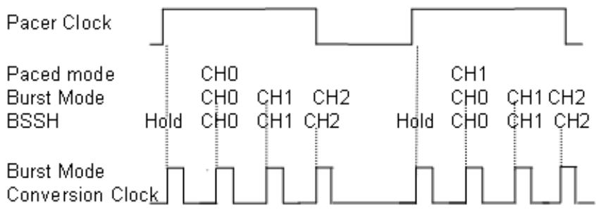
Note: The “HOLD” signal is sent to external S&H circuits to hold the analog signal. There must have an external circuits to carry out the S&H function, there is no on-board device with S&H.
# External Trigger
Through the pin-44 of CN1 (ExtTrig), the A/D conversion also can be performed when a rising edge of external signal is occurred. The conversion rate of this mode is more flexible than the previous two modes, because the users can handle the external signal by outside device. The external trigger can combine with the DMA transfer, interrupt data transfer, or even program polling data transfer. Generally, the interrupt data transfer is often used when external trigger mode is used.
# A/D Data Transfer Modes
On the PCI-9118DG/L, HG/L, HR/L, three A/D data transfer modes can be used when the conversion is completed. The data transfer mode is controlled by the A/D mode control bits (Int, Dma) of the A/D control register (BASE+18). The different data transfer modes are specified as follows:
# Software Data Transfer (ADrdy)
Usually, this mode is used with software A/D trigger mode. After the A/D conversion is triggered by software, the software should poll the ADrdy bit on the A/D Status register until it becomes to high level. Whenever the low byte of A/D data is read, the ADrdy bit will be cleared to indicate the data is read out.
It is possible to read A/D converted data without polling. The A/D conversion time will not excess 8fYs on PCI-9118/L card. Hence, after software trigger, the software can wait for at least 8fYs then read the A/D register without polling.
# Interrupt Transfer (inX)
The PCI-9118/L provides hardware interrupt capability. Under this mode, an interrupt signal is generated when the A/D conversion is ended and the data is ready to be read. It is useful to combine the interrupt transfer with the timer pacer trigger mode. Under this mode, the data transfer is essentially asynchronous with the control software.
When the interrupt transfer is used, the hardware interrupt will be inserted and its corresponding ISR (Interrupt Service Routine) will be invoked and executed after A/D conversion is completed. The converted data is transferred by the ISR program. In PCI design, the IRQ level is assigned by BIOS directly.
# DMA Transfer (Dma)
The DMA (Direct Memory Access) bus master allows data to be transferred directly between the PCI-9118/L and the PC memory at the fastest possible rate, without using any CPU time. The A/D data will be queue at local FIFO on the PCI-9118/L itself and it is automatically transferred to PC's memory.
The DMA transfer mode is very complex to program. It is recommended to use the high level program library to operate this card. If you wish to program the software which can handle the DMA bus master data transfer, please refer to more information about PCI controller.
# Trigger Acquisition Modes
PCI-9118/L provides three types of trigger acquisition modes, pre-trigger, post-trigger and about-trigger. They are described in the following paragraph:
# About-trigger
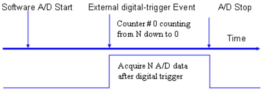
Use about-trigger acquisition in application where you want to collect data before and after a specific trigger event. The digital trigger is input from pin 46 (TGIN) on CN1. To set about trigger mode, set AM bit of A/D Function Register as '1' and specify the 8254 counter0 value. To start the about trigger acquisition, set Start bit of A/D Function Register as '1'. The operation stops when the specified number of samples has been acquired after digital trigger event occurs or DMAStop. The maximum counter0 number can be set is 64K, i.e. After trigger event occurs, the maximum number of data can be accessed is 64K.
# Pre-trigger
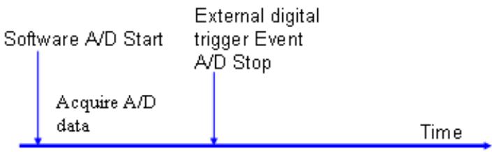
Use pre-trigger acquisition in application where you want to collect data before a specified trigger event. The trigger is a digital trigger which is input from pin 46 (TGIN) on CN1. To set pre-trigger mode, set AM bit of A/D Function Register as '1' and set 8254 counter0 value as 1. To start the pre-trigger, set Start bit of A/D Function Register as '1'. The operation stops after digital -trigger event occurs or DMAStop.
# Post-trigger
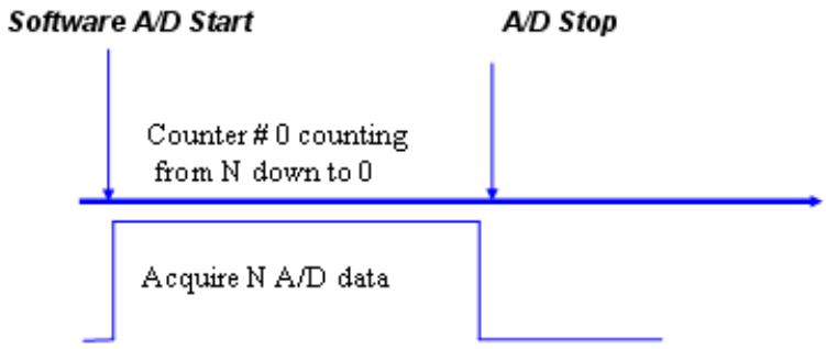
Use post-trigger acquisition in application where you want to collect data after the start condition. To set post-trigger mode, set PM bit of A/D Function Register as '1' and set the 8254 counter0 value. To start the post-trigger, set Start bit of A/D Function Register as '1'. The operation stops after specified number of samples has been acquired or DMAStop. The maximum number of counter0 value can be set is 64K.
# Specifying Channels and Gains in the Channel-Gain Queue
For analog input operation through interrupt and DMA mode, the channel and ranges you want to acquire samples can be specified in a hardware channel-gain queue. You can fill the channel number in the channel-gain queue in consecutive order or in nonconsecutive order. Therefore you can control the channel order for acquiring samples and the gain code for each channel. The maximum number of entries you can set is 255 channels. The channel order for acquiring is the same as the order you set in the channel-gain queue. When the specified channels are read from the first channel to the last channel, the channels in the queue are then sampled again until the specified number of samples is acquired. Please refer to section 6.2 to learn how to use 9118 library to set the channels and gains in the Channel-Gain Queue.
# 5.2 Digital Input and Output
To program digital I/O operation is fairly straight forward. The digital input operation is just to read data from the corresponding registers, and the digital output operation is to write data to the corresponding registers. The digital I/O registers' format are shown in section 4.6. Note that the DIO data channel can only be read or written in form of 16 bits together. It is impossible to access individual bit channel.
# 5.3 Timer/Counter Operation
The PCI-9118/L has an interval timer/counter 8254 on board. Refer to section 3.5 for the signal connection and the configuration of the counters.
# The 8254 Timer / Counter Chip
The Intel (NEC) 8254 contains three independent, programmable, multi-mode 16 bit counter/timers. The three independent 16 bit counters can be clocked at rates from DC to 5 MHz. Each counter can be individually programmed with 6 different operating modes by appropriately formatted control words. The most commonly uses for the 8254 in microprocessor based system are:
▶ programmable baud rate generator
▶ event counter
▶ binary rate multiplier
▶ real-time clock
▶ digital one-shot
▶ motor control
But these three counters are used internally by PCI-9118/L already. There is not a free counter available for general purpose usage. If your application needs to count events or measure frequency, you may consider our PCI-8554 timer/counter card of the details for this card, please visit our website at: http://www.adlink.com.tw and for more information about the 8254, please refer to the NEC Microprocessors and peripherals or Intel Microsystems Components Handbook.
# Pacer Trigger Source
The counter 1 and counter 2 are cascaded together to generate the timer pacer trigger of A/D conversion. The frequency of the pacer trigger is software controllable. The maximum pacer signal rate is 4MHz/4=1000K which exceeds the maximum A/D conversion rate of the PCI-9118/L. The minimum signal rate is 4MHz/65536/65536, which is a very slow frequency that user may never use it.
# Post Counter for About-trigger
The counter0 is used as a post counter. PCI-9118/L provides several acquisition trigger mode. In these trigger modes, about-trigger and post trigger need this counter to count for a specified amount of data that behind the trigger signal. Counter0 is a 16-bit down counter. So, the maximum amount of data that can be acquired after the trigger signal is limited to 64K samples.
# I/O Address
The 8254 in the PCI-9118/L occupies 4 I/O address as shown below.
| BASE + 0x0 | LSB OR MSB OF COUNTER 0 |
| BASE + 0x4 | LSB OR MSB OF COUNTER 1 |
| BASE + 0x8 | LSB OR MSB OF COUNTER 2 |
| BASE + 0xC | CONTROL BYTE |
The programming of 8254 is control by the registers BASE+0 to BASE+C. The functionality of each register is specified this section. For more detailed information, please refer handbook of 8254 chip.
# Control Byte
Before loading or reading any of these individual counters, the control byte (BASE+C) must be loaded first. The format of the control byte is :
| Bit | 7 | 6 | 5 | 4 | 3 | 2 | 1 | 0 |
| SC1 | SC0 | RL1 | RL0 | M2 | M1 | M0 | BCD |
# SC1 & SC0 - Select Counter (Bit7 & Bit 6)
| SC1 | SC0 | COUNTER |
| 0 | 0 | Select Counter 0 |
| 0 | 1 | Select Counter 1 |
| 1 | 0 | Select Counter 2 |
| 1 | 1 | ILLEGAL |
# RL1 & RL0 - Select Read/Load operation (Bit 5 & Bit 4)
| RL1 | RL0 | OPERATION |
| 0 | 0 | COUNTER LATCH FOR STABLE READ |
| 0 | 1 | READ/LOAD LSB ONLY |
| 1 | 0 | READ/LOAD MSB ONLY |
| 1 | 1 | READ/LOAD LSB FIRST, THEN MSB |
# M2, M1 & M0 - Select Operating Mode (Bit 3, Bit 2, & Bit 1)
| M2 | M1 | M0 | MODE |
| 0 | 0 | 0 | 0 |
| 0 | 0 | 1 | 1 |
| x | 1 | 0 | 2 |
| x | 1 | 1 | 3 |
| 1 | 0 | 0 | 4 |
| 1 | 0 | 1 | 5 |
# BCD - Select Binary/BCD Counting (Bit 0)
| 0 | 16-BITS BINARY COUNTER |
| 1 | BINARY COODED DECIMAL (BCD) COUNTER (4 DIGITAL) |
Note The count of the binary counter is from 0 up to 65,535 and the count of the BCD counter is from 0 up to 9,999
# Mode Definitions
In 8254, six operating modes can be selected:
▶ Mode 0 : Interrupt on Terminal Count
▶ Mode 1 : Programmable One-Shot
▶ Mode 2 : Rate Generator
▶ Mode 3 : Square Wave Rate Generator
▶ Mode 4 : Software Triggered Strobe
▶ Mode 5 : Hardware Triggered Strobe
All detailed description of these six modes are written in Intel Microsystems Components Handbook Volume II Peripherals.
# 6 C/C++ Library
This chapter describes the software library for operating this card. Only the functions in DOS library and Windows 95 DLL are described. Please refer to the PCIS-DASK function reference manual, which included in ADLINK CD, for the descriptions of the Windows 98/NT/2000/XP DLL functions.
The function prototypes and some useful constants are defined in the header files LIB directory (DOS) and INCLUDE directory (Windows 95). For Windows 95 DLL, the developing environment can be Visual Basic 4.0 or above, Visual C/C++ 4.0 or above, Borland C++ 5.0 or above, Borland Delphi 2.x (32-bit) or above, or any Windows programming language that allows calls to a DLL. It provides the C/C++, VB, and Delphi included files.
# 6.1 Libraries Installation
Please refer to the "Software Installation Guide" for the detail information about how to install the software libraries for DOS, or Windows 95 DLL, or PCIS-DASK for Windows 98/NT/2000/XP.
The device drivers and DLL functions of Windows 98/NT/2000/XP are included in the PCIS-DASK. Please refer the PCIS-DASK user"s guide and function reference, which included in the ADLINK CD, for detailed programming information.
# 6.2 Programming Guide
# Naming Convention
The functions of the NuDAQ PCI cards or NuIPC CompactPCI cards software driver are using full-names to represent the functions' real meaning. The naming convention rules are:
In a DOS Environment:
```txt
_{hardware_model}_{action_name}. e.g.
_9118_initial().
```
In order to recognize the difference between DOS library and Windows 95 library, a capital "W" is put on the head of each function name of the Windows 95 DLL driver. e.g. W\_9118\_Initial().
# Data Types
We defined some data type in Pci\_9118.h (DOS) and Acl\_pci.h (Windows 95). These data types are used by NuDAQ Cards" library. We suggest you to use these data types in your application programs. The following table shows the data type names and their range.
| Type Name | Description | Range |
| U8 | 8-bit ASCII character | 0 to 255 |
| I16 | 16-bit signed integer | -32768 to 32767 |
| U16 | 16-bit unsigned integer | 0 to 65535 |
| I32 | 32-bit signed integer | -2147483648 to 2147483647 |
| U32 | 32-bit single-precision floating-point | 0 to 4294967295 |
| F32 | 32-bit single-precision floating-point | -3.402823E38 to 3.402823E38 |
| F64 | 64-bit double-precision floating-point | -1.797683134862315E308 to 1.797683134862315E309 |
| Boolean | Boolean logic value | TRUE, FALSE |
# 6.3 \_9118\_Initial
# @ Description
This function is used to initialize PCI-9118/L. Every PCI-9118/L has to be initialized by this function before calling other functions.
@ Syntax
```csv
C/C++ (DOS)
int _9118_Initial (I16 cardNo, I16 *base_address,
I16 *irq_no)
```
C/C++ (Windows 95)
```c
int W_9118_Initial (int cardNo, U16
*base_address1, U16 *base_address2, U8
*irq_no, U8 *pci_master)
```
# Visual Basic (Windows 95)
```txt
W_9118_Initial (ByVal cardNo As Long, base_add1 As Long, base_add2 As Long, irq_no As Byte, pci_master As Byte) As Long
```
# @ Argument
cardNo: the card number of PCI-9118/L to be initialized, totally 4 cards can be initialized, the valid card numbers are PCI\_CARD1, PCI\_CARD2, PCI\_CARD12.
base\_address (DOS): the I/O port base address of the card, it is assigned by system BIOS
op\_base\_address (Win-95): the physical location of S5933 operation Registers in I/O space.
pt\_base\_address (Win-95): the physical location of add-on registers in pass-through I/O space. (This argument is the same as base\_address of DOS version)
irq\_no: the interrupt IRQ level of your PCI-9118/L card, this available irq value is automatically assigned by system BIOS.
pci\_master: BIOS enables or disables bus mastering in PCI Command Register
# @ Return Code
```txt
ERR_NoError
ERR_PCIBiosNotExist
ERR_PCICardNotExist
ERR_PCIIrqNotExist
```
# 6.4 \_9118\_Switch\_Card\_No
# @ Description
This function is used on multi-cards system. After the PCI-9118/L cards are initialized by \_9118\_Initial function, you can use this function to select which one you want to operate. This function is only supported by DOS version.
# @ Syntax
C/C++ (DOS)
int \_9118\_Switch\_Card\_No( int cardNo)
# @ Argument
cardNo: the card number of PCI-9118/L to be initialized, totally 4 cards can be initialized, the valid card numbers are PCI\_CARD1, PCI\_CARD2,..., PCI\_CARD12.
# @ Return Code
ERR\_NoError, ERR\_BoardNoInit
# 6.5 \_9118\_DI
# @ Description
This function is used to read data from digital input port. There are 4 digital input channels on PCI-9118/L. The all 4 bits can be accessed by this function directly.
# @ Syntax
```txt
C/C++ (DOS)
```
```txt
int _9118_DI (unsigned int far *data)
C/C++ (Windows 95)
```
```txt
int W_9118_DI(U16 cardNo, unsigned int *data)
Visual Basic (Windows 95)
```
```txt
W_9118_DI (ByVal cardNo As Integer, data As Long)
As Long
```
# @ Argument
cardNo (Win-95): the card number of PCI-9118/L to be initialized, totally 4 cards can be initialized, the valid card numbers are PCI\_CARD1, PCI\_CARD2,..., PCI\_CARD12.
data:the 4-bit data read from digital port.
# @ Return Code
```txt
ERR_NoError, ERR_BoardNoInit
```
# 6.6 \_9118\_DI\_Channel
# @ Description
This function is used to read data from digital input ports. There are 4 digital input channels on PCI-9118/L. When performing this function, the digital input port is read and the value of the corresponding channel is returned.
# @ Syntax
C/C++ (DOS)
```txt
int _9118_DI_Channel (I16 di_ch_no, unsigned int far *data)
```
C/C++ (Windows 95)
```c
int W_9118_DI_Channel(U16 cardNo, I16 di_ch_no, U16 *data)
```
# Visual Basic (Windows 95)
```txt
W_9118_DI_Channel (ByVal cardNo As Integer, ByVal di_ch_no As Long, data As Long) As Long
```
# @ Argument
cardNo (Win-95): the card number of PCI-9118/L to be initialized, totally 4 cards can be initialized, the valid card numbers are PCI\_CARD1, PCI\_CARD2,..., PCI\_CARD12.
di\_ch\_no: the DI channel number, the valid channel value is from 0 to 3
data :the returned data, either 0 or 1.
# @ Return Code
```txt
ERR_NoError
ERR_BoardNoInit
ERR_InvalidDIChannel
```
# 6.7 \_9118\_DO
# @ Description
This function is used to write data to digital output port. There are 4 output channels on the PCI-9118/L.
# @ Syntax
C/C++ (DOS)
```csv
int _9118_DO (unsigned int data)
C/C++ (Windows 95)
int W_9118_DO (U16 cardNo, U16 data)
Visual Basic (Windows 95)
W_9118_DO (ByVal cardNo As Integer, ByVal data As Long) As Long
```
# @ Argument
cardNo (Win-95): the card number of PCI-9118/L to be initialized, totally 4 cards can be initialized, the valid card numbers are PCI\_CARD1, PCI\_CARD2,..., PCI\_CARD12.
data: the data written to output port.
# @ Return Code
```txt
ERR_NoError
ERR_BoardNoInit
```
# 6.8 \_9118\_AD\_Reset\_AFIFO
# @ Description
This function is used to reset A/D Channel/Gain Register. Before calling \_9118\_AD\_Set\_GainChn (refer to section 6.2.14) to set A/D channel and input range, you have to perform this function to clear A/D Channel/Gain Register.
# @ Syntax
```txt
C/C++ (DOS)
```
```txt
int _9118_AD_Reset_AFIFO()
```
```txt
C/C++ (Windows 95)
```
```txt
int W 9118 AD Reset AFIFO(U16 cardNo)
```
# Visual Basic (Windows 95)
```txt
W_9118_AD_Reset_AFIFO (ByVal cardNo As Integer)
As Long
```
# @ Argument
cardNo (Win-95): the card number of PCI-9118/L to be initialized, totally 4 cards can be initialized, the valid card numbers are PCI\_CARD1, PCI\_CARD2,..., PCI\_CARD12.
# @ Return Code
```txt
ERR_NoError
ERR_BoardNoInit
```
# 6.9 \_9118\_AD\_Bgnset\_AFIFO
# @ Description
Users can not set the A/D channel and input range unless this function is executed. Therefore after this function is performed, the program can start to fill out A/D Channel/Gain register to set the A/D channel and range.
# @ Syntax
C/C++ (DOS)
int 9118 AD Bgnset AFIFO()
C/C++ (Windows 95)
int W\_9118\_AD\_Bgnset\_AFIFO(U16 cardNo)
Visual Basic (Windows 95)
W\_9118\_AD\_Bgnset\_AFIFO (ByVal cardNo As Integer)
As Long
# @ Argument
cardNo (Win-95): the card number of PCI-9118/L to be initialized, totally 4 cards can be initialized, the valid card numbers are PCI\_CARD1, PCI\_CARD2,..., PCI\_CARD12.
# @ Return Code
ERR\_NoError
ERR\_BoardNoInit
# 6.10 \_9118\_AD\_Endset\_AFIFO
# @ Description
This function is used to stop setting A/D channel and input range.
# @ Syntax
```txt
C/C++ (DOS)
```
```txt
int 9118 AD Endset AFIFO()
```
```txt
C/C++ (Windows 95)
```
```txt
int W 9118 AD Endset AFIFO(U16 cardNo)
```
```txt
Visual Basic (Windows 95)
```
```txt
W_9118_AD_Endset_AFIFO (ByVal cardNo As Integer)
As Long
```
# @ Argument
cardNo (Win-95): the card number of PCI-9118/L to be initialized, totally 4 cards can be initialized, the valid card numbers are PCI\_CARD1, PCI\_CARD2,..., PCI\_CARD12.
# @ Return Code
```txt
ERR_NoError
ERR_BoardNoInit
```
# 6.11 \_9118\_AD\_Reset\_DFIFO
# @ Description
This function is used to reset A/D Data FIFO.
# @ Syntax
```csv
C/C++ (DOS)
int _9118_AD_Reset_DFIFO()
C/C++ (DOS)
int W_9118_AD_Reset_DFIFO(U16 cardNo)
Visual Basic (Windows 95)
W_9118_AD_Reset_DFIFO (ByVal cardNo As Integer)
As Long
```
# @ Argument
cardNo (Win-95): the card number of PCI-9118/L to be initialized, totally 4 cards can be initialized, the valid card numbers are PCI\_CARD1, PCI\_CARD2,..., PCI\_CARD12.
# @ Return Code
```txt
ERR_NoError
ERR_BoardNoInit
```
# 6.12 \_9118\_AD\_Set\_Burst\_No
# @ Description
If the A/D conversion mode is set as burst mode, this function is used to set the number of conversion channels in a scan trigger.
# @ Syntax
```txt
C/C++ (DOS)
int 9118_AD_Set_Burst_No(int BurstNo)
C/C++ (Windows 95)
int W_9118_AD_Set_Burst_No(U16 cardNo, int BurstNo)
```
# Visual Basic (Windows 95)
```txt
W_9118_AD_Set_Burst_No (ByVal cardNo As Long, ByVal BurstNo As Integer) As Long
```
# @ Argument
cardNo (Win-95) :the card number of PCI-9118/L to be initialized, totally 4 cards can be initialized, the valid card numbers are PCI\_CARD1, PCI\_CARD2,..., PCI\_CARD12.
BurstNo:the burst number.
# @ Return Code
```txt
ERR_NoError
ERR_BoardNoInit
```
# 6.13 \_9118\_INT\_Set\_CtrlReg
# @ Description
This function is used to set Interrupt Control Register. The definition of each bit of “CtrlVal” is as follows:
| Bit | 7 | 6 | 5 | 4 | 3 | 2 | 1 | 0 |
| -- | -- | -- | -- | Timer | About | Hfull | DTrg |
# @ Syntax
```txt
C/C++ (DOS)
```
```ocaml
int 9118_INT_Set_CtrlReg (int CtrlVal)
```
```txt
C/C++ (Windows 95)
```
```c
int W_9118_INT_Set_CtrlReg(U16 cardNo, int CtrlVal)
```
Visual Basic (Windows 95)
```txt
W_9118_INT_Set_CtrlReg (ByVal cardNo As Long, ByVal CtrlVal As Integer) As Long
```
# @ Argument
cardNo (Win-95): the card number of PCI-9118/L to be initialized, totally 4 cards can be initialized, the valid card numbers are PCI\_CARD1, PCI\_CARD2,..., PCI\_CARD12.
CtrlVal: the value written to Interrupt Control Register.
# @ Return Code
```txt
ERR_NoError
ERR_BoardNoInit
```
# 6.14 \_9118\_AD\_Set\_GainChn
# @ Description
This function is used to specify the A/D channel and input range.
Note: 9118\_AD\_Bgnset\_AFIFO should be called before you use this function to set the channels and gains in the Channel-Gain Queue. After channel setting is finished, you have to call 9118\_AD\_Endset\_AFIFO to stop filling out the Channel-Gain Queue. The sequence to call these three functions is:
```c
_9118_AD_Bgnset_AFIFO();
_9118_AD_Set_GainChn(ch, gain);
:
:
_9118_AD_Set_GainChn(ch, gain);
_9118_AD_Endset_AFIFO();
```
@ Syntax
C/C++ (DOS)
int \_9118\_AD\_Set\_GainChn (int ch, int gain)
C/C++ (Windows 95)
int W\_9118\_AD\_Set\_GainChn(U16 cardNo, int ch, int gain)
Visual Basic (Windows 95)
W\_9118\_AD\_Set\_GainChn (ByVal cardNo As Integer, ByVal ch As Long, ByVal gain As Long) As Long
# @ Argument
cardNo (Win-95): the card number of PCI-9118/L to be initialized, totally 4 cards can be initialized, the valid card numbers are PCI\_CARD1, PCI\_CARD2,..., PCI\_CARD12.
ch: the channel on which perform. operation, the valid value is within 0 to 15.
gain: the A/D input range, the possible values are listed in the column "AD\_INPUT" of the following table.
9118DG/L, HR/L
| AD_INPUT | GAIN | Input Type (Bipolar or Unipolar) | Input Range |
| AD_B_5_V | 1 | Bipolar | „b5V |
| AD_B_2_5_V | 2 | Bipolar | „b2.5V |
| AD_B_1_25_V | 4 | Bipolar | „b1.25V |
| AD_B_0_625_V | 8 | Bipolar | „b0.625V |
| AD_U_10_V | 1 | Unipolar | 0V ~ 10V |
| AD_U_5_V | 2 | Unipolar | 0V ~ 5V |
| AD_U_2_5_V | 4 | Unipolar | 0V ~ 2.5V |
| AD_U_1_25_V | 8 | Unipolar | 0V ~ 1.25V |
9118HG/L
| AD_INPUT | GAIN | Input Type (Bipolar or Unipolar) | Input Range |
| AD_B_5_V | 1 | Bipolar | „b5V |
| AD_B_0_5_V | 10 | Bipolar | „b0.5V |
| AD_B_0_05_V | 100 | Bipolar | „b0.05V |
| AD_B_0_005_V | 1000 | Bipolar | „b0.005V |
| AD_U_10_V | 1 | Unipolar | 0V ~ 10V |
| AD_U_1_V | 10 | Unipolar | 0V ~ 1V |
| AD_U_0_1_V | 100 | Unipolar | 0V ~ 0.1V |
| AD_U_0_01_V | 1000 | Unipolar | 0V ~ 0.01V |
# @ Return Code
```txt
ERR_NoError
ERR_InvalidADChannel
ERR_BoardNoInit
ERR_InvalidADGain
```
# 6.15 \_9118\_AD\_Set\_Scan
# @ Description
This function is used to set the first and last channels in a group of consecutive channels. This function can specify a group of consecutive channels for analog input through DMA and interrupt operation. The sequence of channel scanned is start, start+1, start+2,..., end.
# @ Syntax
C/C++ (DOS)
```txt
Int _9118_AD_Set_Scan(int start, int end, int gain)
```
C/C++ (Windows 95)
```txt
Int W_9118_AD_Set_Scan(U16 cardNo, int start, int end, int gain)
```
Visual Basic (Windows 95)
```txt
W_9118_AD_Set_Scan (ByVal cardNo As Integer, ByVal start As Long, ByVal end As Long, ByVal gain As Long) As Long
```
# @ Argument
cardNo (Win-95): the card number of PCI-9118/L to be initialized, totally 4 cards can be initialized, the valid card numbers are PCI\_CARD1, PCI\_CARD2,..., PCI\_CARD12.
ch: the channel on which perform
start: the First channel number in a group of consecutive channels, the valid value is 0 to 15.
end: the last channel number in a group of consecutive channels, the valid value is 0 to 15.
gain: the A/D input range, the possible values are listed in the column "AD\_INPUT" of the following table.
# @ Return Code
```txt
ERR_NoError
ERR_AD_InvalidChannel
```
ERR\_BoardNoInit
ERR\_InvalidADGain
# 6.16 \_9118\_AD\_Soft\_Trig
# @ Description
This function is used to trigger the A/D conversion by software. This function generates a trigger pulse to PCI-9118/L for A/D conversion and the converted data will be stored in A/D data register.
@ Syntax
```txt
C/C++ (DOS)
int _9118_AD_Soft_Trig ()
C/C++ (Windows 95)
int W_9118_AD_Soft_Trig (U16 cardNo)
Visual Basic (Windows 95)
W_9118_AD_Soft_Trig (ByVal cardNo As Integer) As Long
```
# @ Argument
cardNo (Win-95): the card number of PCI-9118/L to be initialized, totally 4 cards can be initialized, the valid card numbers are PCI\_CARD1, PCI\_CARD2,..., PCI\_CARD12.
# @ Return Code
```txt
ERR_NoError
ERR_BoardNoInit
```
# 6.17 \_9118\_AD\_Set\_Unip
# @ Description
This function is used to set analog input range as uni-polar or bi-polar. The default setting is bi-polar.
# @ Syntax
```c
C/C++ (DOS)
int _9118_AD_Set_Unip (int Unip)
C/C++ (Windows 95)
int W_9118_AD_Set_Unip(U16 cardNo, int Unip)
Visual Basic (Windows 95)
W_9118_AD_Set_Unip (ByVal cardNo As Integer, ByVal Unip As Long) As Long
```
# @ Argument
cardNo (Win-95): the card number of PCI-9118/L to be initialized, totally 4 cards can be initialized, the valid card numbers are PCI\_CARD1, PCI\_CARD2,..., PCI\_CARD12.
Unip: 0: bi-polar
1: uni-polar
# @ Return Code
```txt
ERR_NoError
ERR_BoardNoInit
```
# 6.18 \_9118\_AD\_Set\_Diff
# @ Description
This function is used to set analog input mode as differential or single-ended.
# @ Syntax
```txt
C/C++ (DOS)
int _9118_AD_Set_Diff (int Diff)
C/C++ (Windows 95)
```
```txt
int W_9118_AD_Set_Diff (int Diff)
```
# Visual Basic (Windows 95)
```txt
W_9118_AD_Set_Diff (ByVal cardNo As Integer, ByVal Diff As Long) As Long
```
# @ Argument
cardNo (Win-95): the card number of PCI-9118/L to be initialized, totally 4 cards can be initialized, the valid card numbers are PCI\_CARD1, PCI\_CARD2,..., PCI\_CARD12.
Diff: 0: single-ended
1: differential
# @ Return Code
```txt
ERR_NoError
ERR_BoardNoInit
```
# 6.19 \_9118\_AD\_Set\_SoftG
# @ Description
This function is used to specify the status of software Gate, i.e. it controls 8254 counter to work or stop.
# @ Syntax
```c
C/C++ (DOS)
int _9118_AD_Set_SoftG (int SoftG)
C/C++ (Windows 95)
int W_9118_AD_Set_SoftG(U16 cardNo, int SoftG)
Visual Basic (Windows 95)
W_9118_AD_Set_SoftG (ByVal cardNo As Integer,
ByVal SoftG As Long) As Long
```
# @ Argument
cardNo (Win-95): the card number of PCI-9118/L to be initialized, totally 4 cards can be initialized, the valid card numbers are PCI\_CARD1, PCI\_CARD2,..., PCI\_CARD12.
SoftG: 1: 8254 counter works
0: 8254 counter stops
# @ Return Code
```txt
ERR_NoError
ERR_BoardNoInit
```
# 6.20 \_9118\_AD\_Set\_ExtG
# @ Description
This function is used to specify the A/D control as External Gate control mode or Software Gate Control mode.
# @ Syntax
```txt
C/C++ (DOS)
```
```txt
int 9118 AD Set ExtG (int ExtG)
```
```txt
C/C++ (Windows 95)
```
```txt
int W_9118_AD_Set_ExtG(U16 cardNo, int ExtG)
```
# Visual Basic (Windows 95)
```txt
W_9118_AD_Set_ExtG (ByVal cardNo As Integer, ByVal ExtG As Long) As Long
```
# @ Argument
cardNo (Win-95): the card number of PCI-9118/L to be initialized, totally 4 cards can be initialized, the valid card numbers are PCI\_CARD1, PCI\_CARD2,..., PCI\_CARD12.
ExtG: 1: 8254 counter controlled by TGIN (connector pin 46)
0: 8254 counter controlled by Soft Gate
# @ Return Code
```txt
ERR_NoError
ERR_BoardNoInit
```
# 6.21 \_9118\_AD\_Set\_ExtM
# @ Description
This function is used to specify the hardware trigger source.
# @ Syntax
```txt
C/C++ (DOS)
```
```txt
int 9118 AD Set ExtM (int ExtM)
```
```txt
C/C++ (Windows 95)
```
```txt
int W 9118 AD Set ExtM(U16 cardNo, int ExtM)
```
```txt
Visual Basic (Windows 95)
```
```txt
W_9118_AD_Set_ExtM (ByVal cardNo As Integer, ByVal ExtM As Long) As Long
```
# @ Argument
cardNo (Win-95): the card number of PCI-9118/L to be initialized, totally 4 cards can be initialized, the valid card numbers are PCI\_CARD1, PCI\_CARD2,..., PCI\_CARD12.
ExtM: 1: External Hardware Trigger (connector pin 44).
0: Internal Hardware Trigger.
# @ Return Code
ERR NoError
ERR\_BoardNoInit
# 6.22 \_9118\_AD\_Set\_TmrTr
# @ Description
This function is used to specify the internal trigger source.
# @ Syntax
```txt
C/C++ (DOS)
int _9118_AD_Set_TmrTr (int TmrTr)
C/C++ (Windows 95)
int W_9118_AD_Set_TmrTr (U16 cardNo, int TmrTr)
Visual Basic (Windows 95)
```
```txt
W_9118_AD_Set_TmrTr (ByVal cardNo As Integer, ByVal TmrTr As Long) As Long
```
# @ Argument
cardNo (Win-95): the card number of PCI-9118/L to be initialized, totally 4 cards can be initialized, the valid card numbers are PCI\_CARD1, PCI\_CARD2,..., PCI\_CARD12.
TmrTr:1: 8254 Timer (Counter) is internal trigger source.
0: Software Trigger is internal trigger source.
# @ Return Code
```txt
ERR_NoError
ERR_BoardNoInit
```
# 6.23 \_9118\_AD\_Set\_Int
# @ Description
This function is used to specify the status of interrupt operation. To enable hardware interrupt, "Int" should be set as 1; otherwise the interrupt operation can not be performed.
# @ Syntax
```txt
C/C++ (DOS)
```
```txt
int 9118_AD_Set_Int (int Int)
C/C++ (Windows 95)
```
```txt
int W_9118_AD_Set_Int(U16 cardNo, int Int)
Visual Basic (Windows 95)
```
```txt
W_9118_AD_Set_Int (ByVal cardNo As Integer, ByVal Int As Long) As Long
```
# @ Argument
cardNo (Win-95): the card number of PCI-9118/L to be initialized, totally 4 cards can be initialized, the valid card numbers are PCI\_CARD1, PCI\_CARD2,..., PCI\_CARD12.
Int: 1: Enable Hardware interrupt.
0: Disable Hardware interrupt.
# @ Return Code
```txt
ERR_NoError
ERR_BoardNoInit
```
# 6.24 \_9118\_AD\_Set\_Dma
# @ Description
This function is used to specify the status of DMA transfer mode. To enable DMA Transfer operation, "Dma" should be set as 1; otherwise the DMA operation will not be performed.
# @ Syntax
```txt
C/C++ (DOS)
```
```txt
int 9118 AD Set Dma (int Dma)
```
```txt
C/C++ (Windows 95)
```
```txt
int W 9118 AD Set Dma(U16 cardNo, int Dma)
```
# Visual Basic (Windows 95)
```txt
W_9118_AD_Set_Dma (ByVal cardNo As Integer, ByVal Dma As Long) As Long
```
# @ Argument
cardNo (Win-95): the card number of PCI-9118/L to be initialized, totally 4 cards can be initialized, the valid card numbers are PCI\_CARD1, PCI\_CARD2,..., PCI\_CARD12.
Dma: 1: Enable A/D Data DMA Transfer Mode.
0: Disable A/D Data DMA Transfer Mode.
# @ Return Code
```txt
ERR_NoError
ERR_BoardNoInit
```
# 6.25 \_9118\_AD\_Set\_CtrlReg
# @ Description
This function is used to set the Analog output mode by writing 8 bits data into A/D control register. This function can be used to reset A/D Control Register to default value by setting "CtrlVal" as 0, i.e. the A/D mode is set as bi-polar, single-ended and software trigger). The definition of each bit of "CtrlVal" is as follows:
| Bit | 7 | 6 | 5 | 4 | 3 | 2 | 1 | 0 |
| UniP | Diff | SoftG | ExtG | ExtM | TmrTr | Int | Dma |
# @ Syntax
C/C++ (DOS)
int 9118 AD Set CtrlReg(int CtrlVal)
C/C++ (Windows 95)
int W\_9118\_AD\_Set\_CtrlReg(U16 cardNo, int CtrlVal)
Visual Basic (Windows 95)
W\_9118\_AD\_Set\_CtrlReg (ByVal cardNo As Integer, ByVal CtrlVal As Long) As Long
# @ Argument
cardNo (Win-95): the card number of PCI-9118/L to be initialized, totally 4 cards can be initialized, the valid card numbers are PCI\_CARD1, PCI\_CARD2,..., PCI\_CARD12.
CtrlVal: the value written to A/D control register
# @ Return Code
ERR\_NoError
ERR\_BoardNoInit
# 6.26 \_9118\_AD\_Set\_PDTrg
# @ Description
This function is used to set the active type of digital trigger.
# @ Syntax
```txt
C/C++ (DOS)
int _9118_AD_Set_PDTrg(int PDTrg)
C/C++ (Windows 95)
int W_9118_AD_Set_PDTrg(U16 cardNo, int PDTrg)
Visual Basic (Windows 95)
```
```txt
W_9118_AD_Set_PDTrg (ByVal cardNo As Integer, ByVal PDTrg As Long) As Long
```
# @ Argument
cardNo (Win-95): the card number of PCI-9118/L to be initialized, totally 4 cards can be initialized, the valid card numbers are PCI\_CARD1, PCI\_CARD2,..., PCI\_CARD12.
PDTrg: 0: Negative Trigger.
1: Positive Trigger.
# @ Return Code
```txt
ERR_NoError
ERR_BoardNoInit
```
# 6.27 \_9118\_AD\_Set\_PETrg
# @ Description
This function is used to set the active type of external trigger.
# @ Syntax
```txt
C/C++ (DOS)
```
```c
int _9118_AD_Set_PETrg(int PETrg)
C/C++ (Windows 95)
int W_9118_AD_Set_PETrg(U16 cardNo, int PETrg)
Visual Basic (Windows 95)
```
```txt
W_9118_AD_Set_PETrg (ByVal cardNo As Integer, ByVal PETrg As Long) As Long
```
# @ Argument
cardNo (Win-95): the card number of PCI-9118/L to be initialized, totally 4 cards can be initialized, the valid card numbers are PCI\_CARD1, PCI\_CARD2,..., PCI\_CARD12.
PETrg: 0: Negative Trigger.
1: Positive Trigger.
# @ Return Code
```txt
ERR_NoError
ERR_BoardNoInit
```
# 6.28 \_9118\_AD\_Set\_BSSH
# @ Description
This function is used to enable and disable A/D Burst Mode with Sample and Hold.
# @ Syntax
```txt
C/C++ (DOS)
```
```txt
int 9118 AD Set BSSH (int BSSH)
```
```txt
C/C++ (Windows 95)
```
```txt
int W_9118_AD_Set_BSSH(U16 cardNo, int BSSH)
```
# Visual Basic (Windows 95)
```txt
W_9118_AD_Set_BSSH (ByVal cardNo As Integer, ByVal BSSH As Long) As Long
```
# @ Argument
cardNo (Win-95): the card number of PCI-9118/L to be initialized, totally 4 cards can be initialized, the valid card numbers are PCI\_CARD1, PCI\_CARD2,..., PCI\_CARD12.
BSSH: 0: without Sample and Hold.
1: with Sample and Hold.
# @ Return Code
```txt
ERR_NoError
ERR_BoardNoInit
```
# 6.29 \_9118\_AD\_Set\_BM
# @ Description
This function is used to enable and disable A/D Burst Mode.
# @ Syntax
```txt
C/C++ (DOS)
```
```txt
int 9118 AD Set BM (int BM)
```
```txt
C/C++ (Win95)
```
```txt
int W 9118 AD Set BM(U16 cardNo, int BM)
```
# Visual Basic (Windows 95)
```txt
W_9118_AD_Set_BM (ByVal cardNo As Integer, ByVal BM As Long) As Long
```
# @ Argument
cardNo (Win-95): the card number of PCI-9118/L to be initialized, totally 4 cards can be initialized, the valid card numbers are PCI\_CARD1, PCI\_CARD2,..., PCI\_CARD12.
BM: 0: Normal Mode.
1: Burst Mode.
# @ Return Code
ERR NoError
ERR\_BoardNoInit
# 6.30 \_9118\_AD\_Set\_BS
# @ Description
This function is used to start and stop A/D Burst Mode.
# @ Syntax
```txt
C/C++ (DOS)
```
```txt
int 9118 AD Set BS (int BS)
```
```txt
C/C++ (Windows 95)
```
```txt
int W 9118 AD Set BS(U16 cardNo, int BS)
```
```txt
Visual Basic (Windows 95)
```
```txt
W_9118_AD_Set_BS (ByVal cardNo As Integer, ByVal BS As Long) As Long
```
# @ Argument
cardNo (Win-95): the card number of PCI-9118/L to be initialized, totally 4 cards can be initialized, the valid card numbers are PCI\_CARD1, PCI\_CARD2,..., PCI\_CARD12.
BS: 0: stops Burst Mode.
1: starts Burst Mode.
# @ Return Code
```txt
ERR_NoError
ERR_BoardNoInit
```
# 6.31 \_9118\_AD\_Set\_PM
# @ Description
This function is used to enable and disable Post Trigger Mode.
# @ Syntax
```txt
C/C++ (DOS)
```
```txt
int 9118 AD Set PM (int PM)
```
```txt
C/C++ (Windows 95)
```
```txt
int W 9118 AD Set PM(U16 cardNo, int PM)
```
```txt
Visual Basic (Windows 95)
```
```txt
W_9118_AD_Set_PM (ByVal cardNo As Integer, ByVal PM As Long) As Long
```
# @ Argument
cardNo (Win-95): the card number of PCI-9118/L to be initialized, totally 4 cards can be initialized, the valid card numbers are PCI\_CARD1, PCI\_CARD2,..., PCI\_CARD12.
PM: 0: Disable Post Trigger.
1: Enable Post Trigger.
# @ Return Code
ERR NoError
ERR\_BoardNoInit
# 6.32 \_9118\_AD\_Set\_AM
# @ Description
This function is used to enable and disable About Trigger Mode.
# @ Syntax
```txt
C/C++ (DOS)
```
```solidity
int 9118 AD Set AM (int AM)
```
```txt
C/C++ (Windows 95)
```
```txt
int W_9118_AD_Set_AM(U16 cardNo, int AM)
```
```txt
Visual Basic (Windows 95)
```
```txt
W_9118_AD_Set_AM (ByVal cardNo As Integer, ByVal AM As Long) As Long
```
# @ Argument
cardNo (Win-95): the card number of PCI-9118/L to be initialized, totally 4 cards can be initialized, the valid card numbers are PCI\_CARD1, PCI\_CARD2,..., PCI\_CARD12.
AM 0: Disable About Trigger.
1: Enable About Trigger.
# @ Return Code
```txt
ERR_NoError
ERR_BoardNoInit
```
# 6.33 \_9118\_AD\_Set\_Start
# @ Description
This function is used to start or stop Trigger. After the trigger mode (post-trigger or about trigger) is selected, the program should call this function to start trigger.
# @ Syntax
```txt
C/C++ (DOS)
```
```txt
int _9118_AD_Set_Start (int Start)
C/C++ (Windows 95)
```
```txt
int W_9118_AD_Set_Start(U16 cardNo, int Start)
Visual Basic (Windows 95)
```
```txt
W_9118_AD_Set_Start (ByVal cardNo As Integer, ByVal Start As Long) As Long
```
# @ Argument
cardNo (Win-95): the card number of PCI-9118/L to be initialized, totally 4 cards can be initialized, the valid card numbers are PCI\_CARD1, PCI\_CARD2,..., PCI\_CARD12.
Start: 0: Trigger Stop.
1: Trigger Start.
# @ Return Code
```txt
ERR_NoError, ERR_BoardNoInit
```
# 6.34 \_9118\_AD\_Set\_FuncVal
# @ Description
This function is used to set A/D trigger mode by writing data into A/D Function Register. The definition of each bit is as follows:
| Bit | 7 | 6 | 5 | 4 | 3 | 2 | 1 | 0 |
| PDTrg | PETrg | BSSH | BM | BS | PM | AM | Start |
# @ Syntax
C/C++ (DOS)
int \_9118\_AD\_Set\_FuncReg (int FuncVal)
C/C++ (Windows 95)
int W\_9118\_AD\_Set\_FuncReg(U16 cardNo, int FuncVal)
# Visual Basic (Windows 95)
W\_9118\_AD\_Set\_FuncReg (ByVal cardNo As Integer, ByVal FuncVal As Long) As Long
# @ Argument
cardNo (Win-95): the card number of PCI-9118/L to be initialized, totally 4 cards can be initialized, the valid card numbers are PCI\_CARD1, PCI\_CARD2,..., CI\_CARD12.
FuncVal: the value written to A/D Function Register.
# @ Return Code
ERR\_NoError
ERR\_BoardNoInit
# 6.35 \_9118\_AD\_Aquire
# @ Description
This function is used to poll the A/D conversion data. It will trigger the A/D conversion, and read the A/D data when the data is ready ('data ready' bit becomes low). The value of converted A/D data is from 0 to 4095 (for 9118HG/L, DG/L) or -32768 to 32767(for 9118HR/L).
# @ Syntax
```txt
C/C++ (DOS)
```
```c
int 9118_AD_Aquire ( int far *ad_data )
C/C++ (Windows 95)
int W_9118_AD_Aquire(U16 cardNo, I16 *ad_data )
Visual Basic (Windows 95)
```
```txt
W_9118_AD_Aquire (ByVal cardNo As Integer, ad_data As Integer) As Long
```
# @ Argument
cardNo (Win-95): the card number of PCI-9118/L to be initialized, totally 4 cards can be initialized, the valid card numbers are PCI\_CARD1, PCI\_CARD2,..., PCI\_CARD12.
ad\_data: A/D converted value for PCI-9118DG/L, HG/L, the lowest 4 bits represents the converted channel number and the higher 12 bits is the converted A/D data.
Bit 0 \~ Bit 3: the converted channel number
Bit 4 \~ Bit 15: the converted A/D data
For PCI-9118HR/L, all the 16 bits are the converted A/D data.
# @ Return Code
```txt
ERR_NoError
ERR_BoardNoInit
ERR_AD_AquireTimeOut
```
# 6.36 \_9118\_AD\_DMA\_Start
# @ Description
This function will perform A/D conversion N times with DMA data transfer by using the pacer trigger (internal timer trigger). It takes place in the background which will not stop until the N-th conversion has been completed or your program execute \_9118\_AD\_DMA\_Stop() function to stop the process. The function is performed on single A/D channel when the A/D channel auto-scan is set as FALSE. If the A/D channel auto-scan is TRUE, the conversion will be multiple channels by sequence.
After executing this function, it is necessary to check the status of the operation by using the function \_9118\_AD\_DMA\_Status(). The value of converted A/D data is from 0 to 4095 (9118DG/L, HG/L) or from -32768 to 32767 (9118HR/L).
# @ Syntax
C/C++ (DOS)
```c
int _9118_AD_DMA_Start(int clk_src, unsigned int count, unsigned long *ad_buffer, int c1, int c2)
```
C/C++ (Windows 95)
```txt
int W_9118_AD_DMA_Start(U16 cardNo, int clk_src, unsigned int count, HANDLE memID, int c1, int c2)
```
# Visual Basic (Windows 95)
```txt
W_9118_AD_DMA_Start (ByVal cardNo As Integer,
ByVal clk_src As Long, ByVal count As Long,
ByVal handle As Long, ByVal c1 As Long,
ByVal c2 As Long) As Long
```
# @ Argument
cardNo (Win-95): the card number of PCI-9118/L to be initialized, totally 4 cards can be initialized, the valid card numbers are PCI\_CARD1, PCI\_CARD2,..., PCI\_CARD12.
clk\_src: the clock source for the timer trigger of AD conversion. The valid clock sources are: A\_9118\_AD\_IntSrc, A\_9118\_AD\_ExtSrc
count: the number of A/D conversion in samples.
ad\_buffer (DOS): the start address of the memory buffer to store the A/D data, the buffer size must large than the numbers of A/D conversion. This memory should be double-word alignment.
ad\_buffer is a 32-bit data buffer, but the A/D data is 16-bit format. For PCI-9118/L, the data format of ad\_buffer is as follows:
| DATA1 | DATA0 | DATA3 | DATA2 | ...... | DATAN | DATAN-1 |
Every 16-bit data:
D11 D10 D9 .... D1 D0 C3 C2 C1 C0
Where D11, D10, ., D0: A/D converted data
C3, C2, C1, C0: converted channel no (for 9118DG/L, HG/L)
D15, D14, , D0: A/D converted data (for 9118HR/L)
Please refer to the sample program, ad\_demo3.c, included in the software library CD we provide to get the idea how to get each data sampled (16-bit).
memID (Win-95): the memory ID of the allocated system AI memory. In Windows 95 environment, before calling W\_9118\_AD\_DMA\_Start, W\_9118\_Alloc\_AI\_Mem must be called to allocate a contiguous AI memory. W\_9118\_Alloc\_AI\_Mem will return a memory ID for identify the allocated AI memory, as well as the linear address of the AI memory for user to access the data. The format of the A/D data is the same as DOS buffer (ad\_buff argument).
Note: After the DMA operation stops, the data stored in ad\_buffer or stored in the memory space allocated by memID are the last count transferred data, where count is the value of argument count. Thus, for post trigger mode and about trigger mode, the value of count should be larger than the value of post\_trig\_cnt set in W\_9118\_AD\_Trig to get the all the data transferred during Timer#0 counts down.
c1: the 16-bit timer frequency divider of timer channel #1
c2: the 16-bit timer frequency divider of timer channel #2
Note: the A/D sampling rate is equal to 4MHz / (c1 \* c2).
# @ Return Code
```txt
ERR_NoError
ERR_BoardNoInit
ERR_InvalidADChannel
ERR_InvalidTimerValue
ERR_AD_InvalidGain
```
# 6.37 \_9118\_AD\_DMA\_Status
# @ Description
Since the \_9118\_AD\_DMA\_Start() function executes in background, you can issue this function to check its operation status.
# @ Syntax
```c
C/C++ (DOS)
int _9118_AD_DMA_Status ( int *status, int *count )
C/C++ (Windows 95)
int W_9118_AD_DMA_Status(U16 cardNo, int *status, int *count )
Visual Basic (Windows 95)
```
```txt
W_9118_AD_DMA_Status (ByVal cardNo As Integer, status As Long, count As Long) As Long
```
# @ Argument
cardNo (Win-95): the card number of PCI-9118/L to be initialized, totally 4 cards can be initialized, the valid card numbers are PCI\_CARD1, PCI\_CARD2,..., PCI\_CARD12.
status: status of the DMA data transfer
0: AD\_DMA\_STOP : DMA is completed.
1: AD\_DMA\_RUN : DMA is not completed.
count: the number of A/D data which has been transferred.
# @ Return Code
```txt
ERR_NoError
ERR_AD_DMANotSet
ERR_BoardNoInit
```
# 6.38 \_9118\_AD\_DMA\_Stop
# @ Description
This function is used to stop the DMA data transferring. After executing this function, the internal A/D trigger is disable and the A/D timer (timer #1 and #2) is stopped. The function returns the number of the data which has been transferred, no matter if the A/D DMA data transfer is stopped by this function or by the DMA terminal count ISR.
@ Syntax
```c
C/C++ (DOS)
int _9118_AD_DMA_Stop( int *count, int *start_idx)
C/C++ (Windows 95)
int W_9118_AD_DMA_Stop(U16 cardNo, int *count, int *start_idx )
```
Visual Basic (Windows 95)
```txt
W_9118_AD_DMA_Stop (ByVal cardNo As Integer, count As Long, start_idx As Long) As Long
```
# @ Argument
cardNo (Win-95): the card number of PCI-9118/L to be initialized, totally 4 cards can be initialized, the valid card numbers are PCI\_CARD1, PCI\_CARD2,..., PCI\_CARD12.
count: the number of A/D converted data which has been transferred.
start\_idx: The index where the data start from in user"s buffer, i.e the sequence of read data is:
buff[start\_idx], buff[start\_idx+1], ..., buff[0], buff[1], ..., buff[start\_idx-1].
# @ Return Code
```txt
ERR_NoError
ERR_BoardNoInit
```
# 6.39 \_9118\_ContDmaStart
# @ Description
This function performs continuous A/D conversion with double-buffered DMA data transfer and the pacer trigger (internal timer trigger). It takes place in the background which will not stop until your program execute \_9118\_ContDmaStop() function to stop the process.
After executing this function, it is necessary to check the status of circular buffer by using the function \_9118\_CheckHalfReady() and using \_9118\_DblBufferTransfer() to copy the A/D converted data to transfer buffer.
In current version of software, double-buffered DMA data transfer does not support trigger acquisition mode (pre-trigger, post-trigger, or about-trigger).
There is a group function for continuous A/D conversion using double-buffered DMA transfer as following:
```txt
_9118_ContDmaStart();
_9118_CheckHalfReady();
_9118_DblBufferTransfer();
_9118_GetOverrunStatus();
_9118_ContDmaStop();
```
The value of converted A/D data is from 0 to 4095 (9118DG/L, HG/L) or from 0 to 65535 (9118HR/L).
# @ Syntax
C/C++ (DOS)
```c
_9118_ContDmaStart(int clk_src, unsigned int count, unsigned long *doubleBuf, int c1, int c2)
```
C/C++ (Windows 95)
```txt
W_9118_ContDmaStart(U16 cardNo, int clk_src, unsigned int count, HANDLE memID, int c1, int c2)
```
Visual Basic (Windows 95)
```txt
W_9118_ContDmaStart (ByVal cardNo As Integer, ByVal clk_src, ByVal count As Long, ByVal
```
handle As Long, ByVal c1 As Long, ByVal c2 As Long) As Long
# @ Argument
cardNo (Win-95): the card number of PCI-9118/L to be initialized, totally 4 cards can be initialized, the valid card numbers are PCI\_CARD1, PCI\_CARD2..., PCI\_CARD12.
clk\_src: the clock source for the timer trigger of AD conversion. The valid clock sources are: A\_9118\_AD\_IntSrc, A\_9118\_AD\_ExtSrc
count: the size of circular buffer in samples
db\_buffer (DOS): the start address of the memory of the circular buffer to store the A/D data, the buffer size must large than count.
This memory should be double-word alignment, the ad\_buff format is as following:
ad\_buffer is a 32-bit data buffer, but the A/D data is 16-bit format. For PCI-9118/L, the data format of ad\_buffer is as follows:
| DATA1 | DATA0 | DATA3 | DATA2 | ...... | DATAN | DATAN-1 |
Every 16-bit data:
D11 D10 D9 D1 D0 C3 C2 C1 C0
Where D11, D10, ...D0 : A/D converted data
C3, C2, C1, C0 : converted channel no (for 9118DG/L, HG/L)
D15, D14,...D0: A/D converted data (for 9118HR/L)
Please refer to the sample program, ad\_demo3.c, included in the software library CD we provide to get the idea how to get each data sampled (16-bit).
memID (Win-95): the memory ID of the allocated system AI memory. In Windows 95 environment, before calling W\_9118\_ContDMAStart, W\_9118\_Alloc\_AI\_Mem must be called to allocate a contiguous AI memory. W\_9118\_Alloc\_AI\_Mem will return a memory ID for identify the allocated AI memory, as well as the linear address of the AI memory for user to access the data.
The format of the A/D data is the same as DOS buffer (ad\_buff argument).
c1: the 16-bit timer frequency divider of timer channel #1
c2: the 16-bit timer frequency divider of timer channel #2
Note: The A/D sampling rate is equal to 4MHz / (c1 \* c2).
# @ Return Code
```txt
ERR_NoError
ERR_BoardNoInit,
ERR_InvalidADChannel,
ERR_AD_InvalidGain,
ERR_InvalidTimerValue
```
# 6.40 \_9118\_CheckHalfReady
# @ Description
When you use \_9118\_ContDmaStart() to convert A/D data then you must use \_9118\_CheckHalfReady() to check whether data half full or not in circular buffer, and then can use \_9118\_DblBufferTransfer() to copy data to transfer buffer.
# @ Syntax
C/C++ (DOS)
```c
int _9118_CheckHalfReady(int *halfReady, int *stop_flag)
```
C/C++ (Windows 95)
```c
int W_9118_CheckHalfReady(U16 cardNo, int *halfReady, int *stop_flag)
```
Visual Basic (Windows 95)
```txt
W_9118_CheckHalfReady (ByVal cardNo As Integer, halfReady As Long, stop_flag As Long) As Long
```
# @ Argument
cardNo (Win-95): the card number of PCI-9118/L to be initialized, totally 4 cards can be initialized, the valid card numbers are PCI\_CARD1, PCI\_CARD2,..., PCI\_CARD12.
halfReady: 1 (TRUE) or 0 (FALSE).
stop\_flag: Whether the AD conversion is stopped.
0: not stopped.
1: stopped.
# @ Return Code
```txt
ERR_NoError
```
# 6.41 \_9118\_DblBufferTransfer
# @ Description
Using this function to copy the converted A/D data from circular to transfer buffer. The value of converted A/D data is from 0 to 4095 (9118DG/L, HG/L) or from 0 to 65535 (9118HR/L).
# @ Syntax
C/C++ (DOS)
```c
int _9118_DblBufferTransfer(unsigned short *userBuffer)
C/C++ (Windows 95)
int W_9118_DblBufferTransfer(U16 cardNo, unsigned short *userBuffer)
```
# Visual Basic (Windows 95)
```txt
W_9118_DblBufferTransfer (ByVal cardNo As Integer, userBuffer As Integer) As Long
```
# @ Argument
cardNo (Win-95): the card number of PCI-9118/L to be initialized, totally 4 cards can be initialized, the valid card numbers are PCI\_CARD1, PCI\_CARD2,..., PCI\_CARD12.
userBuffer: user transfer buffer for A/D converted data, every time \_9118\_DblBufferTransfer() copies half size of circular buffer to userBuffer. The size of circular in samples is specified in \_9118\_ContDmaStart() function call.
# @ Return Code
```txt
ERR_NoError
ERR_BoardNoInit
```
# 6.42 \_9118\_GetOverrunStatus
# @ Description
When you use \_9118\_ContDmaStart() to convert A/D data and if you do not use \_9118\_DblBufferTransfer() to copy converted data then the circular buffer overrun will occur. You can use this function to check overrun count.
# @ Syntax
```txt
C/C++ (DOS)
```
```txt
int 9118 GetOverrunStatus(int *overrunCount)
```
```txt
C/C++ (Windows 95)
```
```txt
int W_9118_GetOverrunStatus(U16 cardNo, int *overrunCount)
```
# Visual Basic (Windows 95)
```txt
W_9118_GetOverrunStatus (ByVal cardNo As Integer, overrunCount As Long) As Long
```
# @ Argument
cardNo (Win-95): the card number of PCI-9118/L to be initialized, totally 4 cards can be initialized, the valid card numbers are PCI\_CARD1, PCI\_CARD2,..., PCI\_CARD12.
overrunCount: number of overrun counts.
# @ Return Code
```txt
ERR_NoError
```
# 6.43 \_9118\_ContDmaStop
# @ Description
This function is used to stop the continuous double-buffered DMA data transfer.
# @ Syntax
```csv
C/C++ (DOS)
int _9118_ContDmaStop(unsigned int *count)
C/C++ (DOS)
Int W_9118_ContDmaStop(U16 cardNo, unsigned int *count)
```
# Visual Basic (Windows 95)
```txt
W_9118_ContDmaStop (ByVal cardNo As Integer, count As Long) As Long
```
# @ Argument
cardNo (Win-95): the card number of PCI-9118/L to be initialized, totally 4 cards can be initialized, the valid card numbers are PCI\_CARD1, PCI\_CARD2,..., PCI\_CARD12.
count: the next position after the position the last A/D data is stored in the circular buffer.
# @ Return Code
```txt
ERR_NoError
ERR_BoardNoInit
ERR_AD_DMANotSet
```
# 6.44 \_9118\_AD\_INT\_Start
# @ Description
This function performs A/D conversion N times with interrupt data transfer by using pacer trigger. It takes place in the background which will not stop until the N-th conversion has been completed or your program execute \_9118\_AD\_INT\_Stop() function to stop the process. After executing this function, it is necessary to check the status of the operation by using the function 9118\_AD\_INT\_Status(). The value of A/D converted data is from 0 to 4095 (9118DG/L, HG/L) or from 0 to 65535 (9118HR/L).
# @ Syntax
C/C++ (DOS)
```txt
int _9118_AD_INT_Start( int count, unsigned long
*ad_buffer, int c1, int c2 )
```
C/C++ (Windows 95)
```c
int W_9118_AD_INT_Start(U16 cardNo, int count, HANDLE memID, int c1, int c2)
```
# Visual Basic (Windows 95)
```txt
W_9118_AD_INT_Start (ByVal cardNo As Integer, ByVal count As Long, ByVal handle As Long, ByVal c1 As Long, ByVal c2 As Long) As Long
```
# @ Argument
cardNo (Win-95): the card number of PCI-9118/L to be initialized, totally 4 cards can be initialized, the valid card numbers are PCI\_CARD1, PCI\_CARD2,..., PCI\_CARD12.
count: the number of A/D conversion in samples
ad\_buffer (DOS): the start address of the memory buffer to store the A/D data, the buffer size must large than the number of A/D conversion
This memory should be double-word alignment,
The ad\_buff format is as following: (Note: the ad\_buffer format is not the same as that in 6.2.36. Please refer to sample program ad\_demo 2.c)
| DATA 1 | DATA 2 | DATA 3 | ...... | DATA N |
| 16-bit | 16-bit | 16-bit | | 16-bit |
Every 16-bit data:
D11 D10 D9 .... D1 D0 C3 C2 C1 C0
where D11, D10, ..., D0: A/D converted data
C3, C2, C1, C0: converted channel no (9118DG/L, HG/L)
D15, D14,..., D0: A/D converted data (9118HR/L).
memID (Win-95): the memory ID of the allocated system AI memory. In Windows 95 environment, before calling W\_9118\_AD\_INT\_Start, W\_9118\_Alloc\_AI\_Mem must be called to allocate a contiguous AI memory. W\_9118\_Alloc\_AI\_Mem will return a memory ID for identify the allocated AI memory, as well as the linear address of the AI memory for user to access the data. The format of the A/D data is the same as DOS buffer (ad\_buff argument).
c1: the 16-bit timer frequency divider of timer channel #1
c2: the 16-bit timer frequency divider of timer channel #2
Note: the A/D sampling rate is equal to 4MHz / (c1 \* c2).
# @ Return Code
```txt
ERR_NoError
ERR_BoardNoInit
ERR_InvalidTimerValue
```
# 6.45 \_9118\_AD\_INT\_Status
# @ Description
Since the \_9118\_AD\_INT\_Start() function executes in background, you can issue the function \_9118\_AD\_INT\_Status() to check the status of interrupt operation.
# @ Syntax
```c
C/C++ (DOS)
int _9118_AD_INT_Status( int *status, int *count)
```
C/C++ (Windows 95)
```c
int W_9118_AD_INT_Status(U16 cardNo, int *status, int *count)
```
# Visual Basic (Windows 95)
```txt
W_9118_AD_INT_Status (ByVal cardNo As Integer, status As Long, count As Long) As Long
```
# @ Argument
cardNo (Win-95): the card number of PCI-9118/L to be initialized, totally 4 cards can be initialized, the valid card numbers are PCI\_CARD1, PCI\_CARD2,..., PCI\_CARD12.
status: status of the interrupt data transfer
0: AD\_INT\_INIT : initializes transfer
1: AD\_INT\_RUN :transfer is not completed
2: AD\_INT\_STOP :transfer is completed
count: current conversion count number.
# @ Return Code
```txt
ERR_NoError
ERR_BoardNoInit
```
# 6.46 \_9118\_AD\_INT\_Stop
# @ Description
This function is used to stop the interrupt data transfer function. After executing this function, the internal A/D trigger is disable and the A/D timer is stopped. The function returns the number of the data which has been transferred.
# @ Syntax
C/C++ (DOS)
```c
int 9118_AD_INT_Stop( int *count )
C/C++ (Windows 95)
int W_9118_AD_INT_Stop(U16 cardNo, int *count )
Visual Basic (Windows 95)
```
```txt
W_9118_AD_INT_Stop (ByVal cardNo As Integer, count As Long) As Long
```
# @ Argument
cardNo (Win-95): the card number of PCI-9118/L to be initialized, totally 4 cards can be initialized, the valid card numbers are PCI\_CARD1, PCI\_CARD2,..., PCI\_CARD12.
count: the number of A/D data which has been transferred.
# @ Return Code
```txt
ERR_NoError
ERR_BoardNoInit
ERR_AD_INTNotSet
```
# 6.47 \_9118\_TIMER\_Start
# @ Description
The Timer #0 on the PCI-9118/L can be freely programmed by the users. This function is used to program the Timer #0. This timer can be used as frequency generator if internal clock is used. It also can be used as event counter if external clock is used.
@ Syntax
```txt
C/C++ (DOS)
int _9118_TIMER_Start( int timer_mode, unsigned int c0 )
C/C++ (Windows 95)
int W_9118_TIMER_Start(U16 cardNo, int timer mode, U16 c0 )
```
Visual Basic (Windows 95)
```txt
W_9118_TIMER_Start (ByVal cardNo As Integer, ByVal timer_mode As Long, ByVal c0 As Long) As Long
```
# @ Argument
cardNo (Win-95): the card number of PCI-9118/L to be initialized, totally 4 cards can be initialized, the valid card numbers are PCI\_CARD1, PCI\_CARD2,..., PCI\_CARD12.
timer\_mode: the 8254 timer mode, the possible values are:
```txt
TIMER_MODE0, TIMER_MODE1,
TIMER_MODE2, TIMER_MODE3,
TIMER_MODE4, TIMER_MODE5.
```
c0: the counter value of timer
# @ Return Code
```txt
ERR_NoError
ERR_BoardNoInit
ERR_InvalidTimerMode
```
Note: If TIMER\_MODE4 is used, C0 is one smaller than the counter number you specify. That is, if the counter number you specify is 100, the C0 is set as 99.
# 6.48 \_9118\_TIMER\_Read
# @ Description
This function is used to read the counter value of the Timer #0.
# @ Syntax
```c
C/C++ (DOS)
int _9118_TIMER_Read( unsigned int *counter_value )
C/C++ (Windows 95)
int W_9118_TIMER_Read(U16 cardNo, unsigned int *counter value)
```
# Visual Basic (Windows 95)
```txt
W_9118_TIMER_Read (ByVal cardNo As Integer, counter_value As Long) As Long
```
# @ Argument
cardNo (Win-95): the card number of PCI-9118/L to be initialized, totally 4 cards can be initialized, the valid card numbers are PCI\_CARD1, PCI\_CARD2,..., PCI\_CARD12.
counter\_value: the counter value of the Timer #0
# @ Return Code
```txt
ERR_NoError
ERR_BoardNoInit
```
# 6.49 \_9118\_TIMER\_Stop
# @ Description
This function is used to stop the timer operation. The timer is set to the 'One-shot' mode with counter value '0'. That is, the clock output signal will be set to high after executing this function.
@ Syntax
```txt
C/C++ (DOS)
int _9118_TIMER_Stop(unsigned int *counter_value)
```
C/C++ (Windows 95)
```c
int W_9118_TIMER_Stop(U16 cardNo, unsigned int *counter value)
```
Visual Basic (Windows 95)
```txt
W_9118_TIMER_Stop (ByVal cardNo As Integer, counter_value As Long) As Long
```
# @ Argument
cardNo (Win-95): the card number of PCI-9118/L to be initialized, totally 4 cards can be initialized, the valid card numbers are PCI\_CARD1, PCI\_CARD2,..., PCI\_CARD12.
counter\_value: the current counter value of the Timer #0.
@ Return Code
```txt
ERR_Board_NoInit
ERR_NoError
```
# 6.50 W\_9118\_Set\_Trig
# @ Description
This function is used to set up a trigger. The function specifies the trigger mode and post trigger count. Please refer to section 5.1.4 for the detailed description of trigger setting. This function is only supported by Windows 95 version.
# @ Syntax
C/C++ (Windows 95)
```c
Int W_9118_Set_Trig(U16 cardNo, int trig_mode, U16 post_trig_cnt)
```
Visual Basic (Windows 95)
```txt
W_9118_Set_Trig (ByVal cardNo As Integer, ByVal trig_mode As Integer, ByVal post_trig_cnt As Long) As Long
```
# @ Argument
cardNo: the card number of PCI-9118/L to be initialized, the valid card numbers are PCI\_CARD1, PCI\_CARD2,..., PCI\_CARD12.
trig\_mode: selected trigger mode. The valid values are the following:
SOFT\_TRIG: Software trigger
POST\_TRIG: Post trigger
PRE\_TRIG: Pre-trigger
ABOUT\_TRIG: About trigger
post\_trig\_cnt: The post trigger count. it will count down the Timer#0 after the trigger condition was met (About trigger) or at the moment DMA operation starts(Post-trigger). When the count reaches 0, the counter stops. The counter is used to control the post trigger sampling count of about trigger and control the sampling count of post trigger mode. For Pre-trigger mode, this argument has to be set as 1.
Note: For post trigger mode and about trigger mode, the value of post\_trig\_cnt should be smaller than the value of count set in
9118\_AD\_DMA\_Start to get the all the data transferred during Timer#0 counts down. Please refer to section 6.2.36 for the detailed description.
# @ Return Code
PCICardNumErr
PCICardNotInit
InvalidClkDiv
NoError
# 6.51 W\_9118\_Alloc\_AI\_Mem
# @ Description
Contact Windows 95 system to allocate a block of contiguous memory for continuous AI transfer. This function is only available in Windows 95 version.
# @ Syntax
C/C++ (Windows 95)
```c
int W_9118_Aloc_AI_Mem (U32 buf_size, HANDLE *memID, U32 *linearAddr, U32 *phyAddr)
```
# Visual Basic (Windows 95)
```txt
W_9118_Alloc_AI_Mem (ByVal buf_size As Long, memID As Long, linearAddr As Long, phyAddr As Long) As Long
```
# @ Argument
buf\_size: Bytes to allocate. Please be careful, the unit of this argument is BYTE, not SAMPLE.
memID: If the memory allocation is successful, driver returns the ID of that memory in this argument. Use this memory ID in W\_9118\_AD\_DMA\_Start, W\_9118\_AD\_INT\_Start and W\_9118\_ContDmaStart function calls.
linearAddr: The linear address of the allocated AI memory. You can use this linear address as a pointer in C/C++ to access the AI data.
phyAddr: The physical address of the allocated AI memory.
# @ Return Code
```txt
NoError
AllocDMAMemFailed
```
# 6.52 W\_9118\_Free\_AI\_Mem
# @ Description
De-allocate a system AI memory under Windows 95 environment. This function is only available in Windows 95 version.
# @ Syntax
C/C++ (Windows 95)
int W 9118 Free AI Mem (HANDLE memID)
Visual Basic (Windows 95)
W\_9118\_Free\_AI\_Mem (ByVal memID As Long) As Long
# @ Argument
memID: The memory ID of the system AI memory to deallocate.
# @ Return Code
NoError
# 6.53 W\_9118\_Get\_Sample
# @ Description
For the language without pointer support such as Visual Basic, programmer can use this function to access the index-th data in AI buffer.
# @ Syntax
C/C++ (Windows 95)
```c
int W_9118_Get_Sample (U32 linearAddr, U32 index, I16 *ai_data)
```
Visual Basic (Windows 95)
```txt
W_9118_Get_Sample (ByVal linearAddr As Long, ByVal idx As Long, ai_data As Integer) As Long
```
# @ Argument
linearAddr: The linear address of the allocated AI memory.
index: The index of the sample. The first sample is with index 0.
ai\_data: Returns the sample retrieved.
# @ Return Code
NoError
# 7 Calibration
In data acquisition process, how to calibrate your measurement devices to maintain its accuracy is very important. Users can calibrate the analog input and analog output channels under the users' operating environment for optimizing the accuracy. This chapter will guide you to calibrate your PCI-9118/L to an accuracy condition.
# 7.1 What do you need
Before calibrating your PCI-9118/L card, you should prepare some equipment's for the calibration:
▶ Calibration program: Once the program is executed, it will guide you to do the calibration. This program is included in the delivered package
▶ A 5 1/2 digit multimeter (6 1/2 is recommended)
▶ A voltage calibrator or a very stable and noise free DC voltage generator
# 7.2 VR Assignment
There are five variable resistors (VR) on the PCI-9118/L board to allow you making accurate adjustment on A/D channels. The function of each VR is specified as Table 7.1.
| VR5 | A/D full scale adjustment |
| VR6 | A/D bipolar offset adjustment |
| VR7 | A/D unipolar offset adjustment |
Table 7-1: VRs Functions
# 7.3 A/D Adjustment
# Bipolar Calibration
1. Set the analog input range as: $\pm5V$ , i.e. the gain = 1 and input mode = Bipolar.
2. Connect A/D channel 0 (pin 26 of CN1) to ground (pin 34 of CN1), and Applied a +5V to A/D channel 1 (pin 27 of CN1).
3. Trim VR6 to obtain the reading of A/D channel 0 flicks between 2048\~2049 (9118DG/L, HG/L) or 0 to 1 (9118HR/L), and Trim VR5 to obtain reading of A/D channel 1 flicks between 4094\~4095 (9118DG/L, HG/L) or 32766\~32767 (9118HR/L).
# Unipolar Calibration
1. Set the analog input range as: 0 \~ 10 V, i.e. the gain = 1 and input mode = Unipolar.
2. Applied a +5 V input signal to A/D channel 0, and trim the VR7 to obtain reading flicking between 2047\~2048 (9118DG/L, HG/L) or 0\~1 (9118HR/L).
# 8 Software Utility
This software CD provides a utility program, 9118util.exe which provides three functions, System Configuration, Calibration, and Functional Testing. This utility is designed as menu-driven based windowing style. Not only the text messages are shown for operating guidance, but also has the graphic to indicate you how to set right hardware configuration. This utility is described in the following sections.
# 8.1 Running 9118util.exe
After finishing the DOS installation, you can execute the utility by typing as follows (assume your utility is located in \ADLINK\DOS\9118\Util directory):
```txt
C> cd \ADLINK\DOS\9118\Util
C> 9118UTIL
```
the following diagram will be displayed on you screen. The message at the bottom of each window guides you how to select item, go to next step and change the default settings.
Note: all the D/A functions mentioned in this utility is useless.
```txt
***** PCI-9118 Utility Rev. 1.0 *****
Copyright © 1995-1997, ADLINK Technology Inc. All rights reserved.
```
```erb
<F1>: Configuration.
<F2>: Calibration.
<F3>: Function testing.
<Esc>: Quit.
```
```html
>>> Select function key F1 ~ F3, or press <Esc> to quit. <<
```
# 8.2 System Configuration
This function guides you to configure the PCI-9118/L card, and set the right hardware configuration. The configuration window shows the setting items that you have to set before using the PCI-9118/L card.
The following diagram will be displayed on the screen as you choose the Configuration function from main menu.
\*\*\*\*\* Calibration of PCI9118 \*\*\*\*\*
<table> |
| <1> Card Type 9118DG |
| <2> ADC Trigger Source Internal |
| <3> Timer Clock Source Internal |
| <4> AD Input Channel Config Single-Ended |
| <5> AD Polarity setting Bipolar |
| <6> AD Input Range Gain=1 Bipolar(-5V~5V) |
|
>>> <Up/Down>: Select Item, <PgUp/PgDn>: Change Setting <<
# 8.3 Calibration
This function guides you to calibrate the PCI-9118/L. The calibration program serves as a useful test of the PCI-9118/L's A/D and DIO functions and can aid in troubleshooting if problems arise.
Note: For an environment with frequently large changes of temperature and vibration, a 3 months re-calibration interval is recommended. For laboratory conditions, 6 months to 1 year is acceptable.
When you choose the calibration function from the main menu list, a calibration items menu is displayed on the screen. After you select one of the calibration items from the calibration items menu, a calibration window shows. The upper window shows the detailed procedures which have to be followed when you proceed the calibration. The instructions will guide you to calibrate each item step by step. The bottom window shows the layout of PCI-9118/L. In addition, the proper Variable Resister (VR) will blink to indicate the related VR which needs to be adjusted for the current calibration step.
```txt
***** PCI-9118 Calibration *****
```
```txt
<1> D/A channel 1 voltage full range adjusting
<2> D/A channel 2 voltage full range adjusting
<3> A/D (Bipolar Gain = 1, -5V ~ 5V) adjusting
<4> A/D (Unipolar Gain = 1, -5V ~ 5V) adjusting
<Esc> Quit
```
Select 1 to 4 or <Esc> to quit calibration.
If you select 3, the following figure displays on the screen:
A/D (Bipolar, Gain = 1, -5V\~5V) adjusting
```txt
Step 1: Connect CN1.AI0 (PIN 26) to CN1.GND (PIN 34)
Input 5V to CN1.AI1 (PIN 27)
Step 2: Trim VR6 until the value of AI0 is jumping from 2048 to 2049
Trim VR5 until the value of AI1 is jumping from 4094 to 4095
```
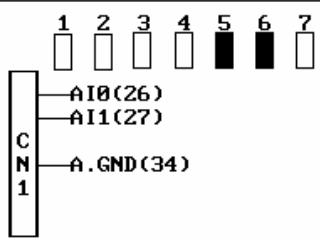
```txt
CH0 =2055
CH1 =4095
```

<ENTER> Completed AD Bipolar calibration.
<F10> Completed AD Bipolar calibration, otherwise repeat Step 1 to 4.
# 8.4 Functional Testing
This function is used to test the functions of PCI-9118/L, it includes Digital I/O testing, A/D polling testing, A/D Interrupt Testing, A/D with DMA testing, A/D with DMA & Burst Mode testing, A/D with DMA & BSSH testing, and A/D with DMA & post-trigger testing.
When you choose one of the testing function from the functions menu, a diagram is displayed on the screen. The figures below are the function testing menu window and A/D with Polling Testing window.
\*\*\*\*\* PCI-9118 Function Testing \*\*\*\*\*
| <1>: DI/DO Test |
| <2>: D/A Test |
| <3>: A/D with Polling Test |
| <4>: A/D with Interrupt Test |
| <5>: A/D with DMA Test |
| <6>: A/D with DMA & Burst Mode |
| <7>: A/D with DMA & BSSH |
| <8>: A/D with DMA & post-trigger |
| <Esc>: Quit |
Select 1 to 8 or <Esc> to quit function testing
Figure 8-1: Function Testing Menu Window
```txt
******** ACL-9118DG/HG Utility Rev. 1.0 *****
```
```txt
Copyright (c) 1995-1997, ADLink Technology Inc. All rights reserved.
```
```txt
<1> Connected input source to CN1.AI0, CN1.A.GND and CN1.AI1, CN1.A.GND
== Software Poll A/D Channel 0, 1 ==
Channel 0 = 2048 = 0.6012 Volt.
Channel 1 = 1910 = -0.3358 Volt.
```
```txt
>>> Press <ESC> to stop <<<
```
Figure 8-2: A/D with Polling Test window
A calibration utility is supported in the software CD which is included in the product package. The detailed calibration procedures and description can be found in the utility. Users only need to run the software calibration utility and follow the procedures. You will get the accurate measure data.
In normal condition, the PCI-9118/L already calibrated by factor before it is shipped out. So, users do not need to calibrate your PCI-9118/L when you get it.
# Warranty Policy
Thank you for choosing ADLINK. To understand your rights and enjoy all the after-sales services we offer, please read the following carefully.
1. Before using ADLINK's products please read the user manual and follow the instructions exactly. When sending in damaged products for repair, please attach an RMA application form which can be downloaded from: http://rma.adlinktech.com/policy/.
2. All ADLINK products come with a two-year guarantee:
The warranty period starts from the product's shipment date from ADLINK's factory.
▶ Peripherals and third-party products not manufactured by ADLINK will be covered by the original manufacturers' warranty.
For products containing storage devices (hard drives, flash cards, etc.), please back up your data before sending them for repair. ADLINK is not responsible for loss of data.
▶ Please ensure the use of properly licensed software with our systems. ADLINK does not condone the use of pirated software and will not service systems using such software. ADLINK will not be held legally responsible for products shipped with unlicensed software installed by the user.
For general repairs, please do not include peripheral accessories. If peripherals need to be included, be certain to specify which items you sent on the RMA Request & Confirmation Form. ADLINK is not responsible for items not listed on the RMA Request & Confirmation Form.
3. Our repair service is not covered by ADLINK's two-year guarantee in the following situations:
▶ Damage caused by not following instructions in the user's manual.
▶ Damage caused by carelessness on the user's part during product transportation.
▶ Damage caused by fire, earthquakes, floods, lightening, pollution, other acts of God, and/or incorrect usage of voltage transformers.
▶ Damage caused by unsuitable storage environments (i.e. high temperatures, high humidity, or volatile chemicals).
▶ Damage caused by leakage of battery fluid during or after change of batteries by customer/user.
▶ Damage from improper repair by unauthorized technicians.
▶ Products with altered and/or damaged serial numbers are not entitled to our service.
▶ Other categories not protected under our warranty.
4. Customers are responsible for shipping costs to transport damaged products to our company or sales office.
5. To ensure the speed and quality of product repair, please download an RMA application form from our company website: http://rma.adlinktech.com/policy. Damaged products with attached RMA forms receive priority.
If you have any further questions, please email our FAE staff: service@adlinktech.com.
[🔗 Link to the original document](.pci-9118-lseries-manual-3/pci-9118-lseries-manual-3.pdf)