# NuDAQ PCI-9812/9810

4-CH, 20 MHz Simultaneous

Analog Input Card

User's Manual

Manual Rev. 3.02

Revision Date: December 2, 2008

Part No: 50-11116-2040

![The image displays the universal recycling symbol. It features a black circle containing three white, curved arrows arranged in a triangular formation. The arrows are stylized to look like a continuous ribbon, chasing each other in a clockwise direction.](.pci-9812-9810-50-11116-2040-302/1e5a21031c4b3f876fbd8d9afa4f7259f2baf8ec3c3c0f257837468f538034c2.jpg)
Recycled Paper

Copyright 2008 ADLINK TECHNOLOGY INC.

All Rights Reserved.

# Disclaimer

The information in this document is subject to change without prior notice in order to improve reliability, design, and function and does not represent a commitment on the part of the manufacturer.

In no event will the manufacturer be liable for direct, indirect, special, incidental, or consequential damages arising out of the use or inability to use the product or documentation, even if advised of the possibility of such damages.

This document contains proprietary information protected by copyright. All rights are reserved. No part of this manual may be reproduced by any mechanical, electronic, or other means in any form without prior written permission of the manufacturer.

# Trademark Information

NuDAQ, NuIPC, DAQBench are registered trademarks of ADLINK TECHNOLOGY INC.

Product names mentioned herein are used for identification purposes only and may be trademarks and/or registered trademarks of their respective companies.

# Getting service

Customer satisfaction is our top priority. Contact us should you require any service or assistance.

# ADLINK TECHNOLOGY INC.

Web Site http://www.adlinktech.com

Sales & Service service@adlinktech.com

Telephone No. +886-2-8226-5877

Fax No. +886-2-8226-5717

Mailing Address 9F No. 166 Jian Yi Road, Chungho City,

Taipei Hsien 235, Taiwan

# ADLINK TECHNOLOGY AMERICA, INC.

Sales & Service info@adlinktech.com

Toll-Free +1-866-4-ADLINK (235465)

Fax No. +1-949-727-2099

Mailing Address 8900 Research Drive, Irvine,

CA 92618, USA

# ADLINK TECHNOLOGY EUROPEAN SALES OFFICE

Sales & Service emea@adlinktech.com

Toll-Free +49-211-4955552

Fax No. +49-211-4955557

Mailing Address    Nord Carree 3, 40477 Düsseldorf, Germany

# ADLINK TECHNOLOGY SINGAPORE PTE LTD.

Sales & Service singapore@adlinktech.com

Telephone No. +65-6844-2261

Fax No. +65-6844-2263

Mailing Address 84 Genting Lane #07-02A,

Cityneon Design Center, Singapore 349584

# ADLINK TECHNOLOGY SINGAPORE PTE LTD.

# (INDIA Liaison Office)

Sales & Service india@adlinktech.com

Telephone No. +91-80-57605817

Fax No. +91-80-26671806

Mailing Address No. 1357, Ground Floor, "Anupama",

Aurobindo Marg JP Nagar (Ph-1)

Bangalore - 560078

# ADLINK TECHNOLOGY INC. (KOREA Liaison Office)

Sales & Service korea@adlinktech.com

Telephone No. +82-2-20570565

Fax No. +82-2-20570563

Mailing Address 4F, Kostech Building, 262-2,

Yangjae-Dong, Seocho-Gu,

Seoul, 137-130, South Korea

# ADLINK TECHNOLOGY (BEIJING) CO., LTD.

Sales & Service market@adlinkchina.com.cn

Telephone No. +86-10-5885-8666

Fax No. +86-10-5885-8625

Mailing Address Room 801, Building E, Yingchuangdongli

Plaza, No.1 Shangdidonglu,

Haidian District, Beijing, China

# ADLINK TECHNOLOGY (SHANGHAI) CO., LTD.

Sales & Service market@adlinkchina.com.cn

Telephone No. +86-21-6495-5210

Fax No. +86-21-5450-0414

Mailing Address Floor 4, Bldg. 39, Caoheting Science and

Technology Park, No.333 Qinjiang Road,

Shanghai, China

# ADLINK TECHNOLOGY (SHENZEN) CO., LTD.

Sales & Service market@adlinkchina.com.cn

Telephone No. +86-755-2643-4858

Fax No. +86-755-2664-6353

Mailing Address C Block, 2nd Floor, Building A1,

Cyber-tech Zone, Gaoxin Ave. 7.S,

High-tech Industrial Park S.,

Nanshan District, Shenzhen,

Guangdong Province, China

# Using this manual

# Audience and scope

This manual guides you when using ADLINK NuDAQ® multi-function PCI card. The card's hardware, signal connections, and calibration information are provided for faster application building. This manual is intended for computer programmers and hardware engineers with advanced knowledge of data acquisition and high-level programming.

# How this manual is organized

This manual is organized as follows:

Chapter 1 Introduction: This chapter introduces the PCI-9812/9810 card including its features, specifications, software support information, and package contents.

Chapter 2 Hardware Information: This chapter presents the card's layout and connector pin definition.

Chapter 3 Installation: This part describes the PCI-9812/9810 installation, configuration, and options for signal connections.

Chapter 4 Registers: Descriptions of the register format and structure of the PCI-9812/9810 are specified in this chapter.

Chapter 5 Operation Theory: The operation theory of the PCI-9221 functions including A/D conversion, D/A conversion, and programmable function I/O are discussed in this chapter.

Chapter 6 Function Reference: The chapter includes a software library necessary for operating the PCI-9812/9810 card in DOS or Windows 95.

Chapter 7 Calibration: The chapter offers information on how to calibrate the PCI-9812/9810 for accurate data acquisition and output.

Chapter 8 Software Utility: The chapter offers information on how to use the software utility to configure, calibrate, and test the PCI-9812/9810 card.

Warranty Policy: This presents the ADLINK Warranty Policy terms and coverages.

# Conventions

Take note of the following conventions used throughout the manual to make sure that you perform certain tasks and instructions properly.

NOTE Additional information, aids, and tips that help you perform particular tasks.

IMPORTANT Critical information and instructions that you MUST perform to complete a task.

WARNING Information that prevents physical injury, data loss, module damage, program corruption etc. when trying to complete a particular task.

# Table of Contents

# List of Tables...... iv

# List of Figures ...... v

# 1 Introduction ...... 1

1.1 Features.... 1
1.2 Applications ...... 1
1.3 Specifications.... 2
1.4 Unpacking Checklist 4
1.5 Software Support 5
Software Support 5
Programming Libraries 5
Drivers for Third-Party Programming Languages ...... 6

# 2 Hardware Information 9

2.1 Layout 9
2.2 Connectors 10
JP1 Pin Definition 11
2.3 Input Settings.... 12
Analog Input 12
External Clock 0 14
External Clock 1 14
Digital Input 14

# 3 Installation 15

3.1 Before You Proceed 15
3.2 Installing the Card.... 15
3.3 Configuring the Card.... 16
Troubleshooting 16
3.4 Installing the Drivers for Windows 16

# 4 Registers.... 17

4.1 I/O Port Address 17
ADC Channel Enable Register 18
ADC Clock Divisor Register 19
Trigger Mode Register 20
Trigger Level Register 21
Trigger Source Register 22

Post Trigger Counter Register 23

FIFO Status Register 24

FIFO Control Register 25

Acquisition Enable Register 26

Clock Source Register 27

4.2 High Level Programming 28

4.3 Low Level Programming 28

# 5 Operation Theory 29

5.1 Conversion Procedure 29

5.2 Signal Source Control 31

5.3 Trigger Source Control.... 32

Trigger Sources 32

Trigger Modes 34

5.4 Clock Source Control 36

A/D Clock Sources 36

5.5 Data Transfer 38

Data Transfer 38

Simultaneous Sampling of Four AD Channels 38

Total Data Throughput 39

Maximum Acquiring Data Length 39

Bus-mastering Data Transfer 40

Host Memory Operation 40

5.6 Data Format 42

# 6 Function Reference 45

6.1 Installing the Libraries 45

6.2 Programming Guide.... 46

Naming Convention 46

Data Types 47

6.3 Function Reference.... 48

\_9812\_Initial 48

\_9812\_Close 50

\_9812\_AD\_DMA\_Start 51

\_9812\_AD\_DMA\_Status 54

\_9812\_AD\_DMA\_Stop 55

\_9812\_Set\_Clk\_Src 56

\_9812\_Set\_Clk\_Rate 57

\_9812\_Set\_Trig 58

W\_9812\_Alloc\_DMA\_Mem 60

W\_9812\_Free\_DMA\_Mem 61

W\_9812\_Get\_Sample 62

# 7 Calibration.... 63

7.1 Before You Proceed 63
7.2 VR Assignment 63
7.3 A/D Calibration.... 64

A/D Calibration for Channel 0 64

A/D Calibration for Channels 1/2/3 64

# 8 Software Utility 65

8.1 Running the Utility.... 65
8.2 System Configuration 66
8.3 Calibration.... 67
8.4 Functional Testing 69

# List of Tables

Table 2-1: JP1 Pin Definition 11

Table 2-2: JP1 Pin Definition Connected to 9-pin D-type Connector .... 11

Table 2-3: Analog Input 12

Table 2-4: Switches and Resistors 13

Table 4-1: I/O Address 17

Table 4-2: Five Trigger Modes 20

Table 6-1: Data Types 47

Table 7-1: Functions of VRs 63

Table 7-2: AD Calibration for Channels 1/2/3 64

# List of Figures

Figure 2-1: Location of Connectors.... 10

Figure 5-1: Post-trigger Acquisition.... 34

Figure 5-2: Pre-trigger Acquisition 34

Figure 5-3: Middle-trigger Acquisition 35

Figure 5-4: Delay-trigger Acquisition.... 35

Figure 5-5: Data Transfer Diagram of PCI-9812/9810.... 38

# 1 Introduction

The PCI-9812/9810 is an advanced performance data acquisition card based on the 32-bit PCI bus architecture. With maximum sampling rate of up to 20 million samples per second, the PCI-9812/9810 delivers continuous and high-speed streaming of A/D samples to the host memory. The high-performance design and state-of-the-art technology make these cards ideal for DSP, FFT, digital filtering, and image processing applications.

# 1.1 Features

The PCI-9812/9810 advanced DAQ card is designed with the following features:

▶ 32-bit PCI bus with bus mastering DMA data transfer
▶ 12-bit (PCI-9812)/10-bit (PCI-9810) analog input resolution
▶ Onboard 32K words (samples) A/D FIFO memory
▶ Up to 20 MHz A/D sampling rate
▶ Four single-ended analog input channels
▶ Bipolar input signals
▶ Four A/D converters with simultaneously sampling
▶ Five A/D trigger modes including software trigger, pre-trigger, post-trigger, middle trigger, and delay trigger

# 1.2 Applications

▶ IF and BASEBAND digitization
▶ Ultrasound imaging
▶ Gamma cameras
▶ Test instrument
▶ CCD imaging
▶ Video digitizing

# 1.3 Specifications

<table><tr><td colspan="2">Analog Input (AI)</td></tr><tr><td>Converters</td><td>B.B. ADS800 series</td></tr><tr><td>Input Channels</td><td>Four single-ended</td></tr><tr><td>Resolution</td><td>12-bit (PCI-9812)10-bit (PCI-9810)</td></tr><tr><td>Over Voltage Protection</td><td>Bipolar ±1 V, or ±5 V by soldering selection</td></tr><tr><td>Maximum Sampling Rate $^{1}$ </td><td>20 MHz samples/second</td></tr><tr><td>Accuracy</td><td>Gain error ±1.5% at 25°C</td></tr><tr><td>Input Impedance (soldering selectable)</td><td>50 Ω (±1 V and ±5 V)1.25 KΩ (±5 V only)5 MΩ (±1 V only)</td></tr><tr><td colspan="2">Dynamic Characteristic</td></tr><tr><td>Differential Linearity Error</td><td>±0.4 LSB (Typ.) ±1.0 LSB (Max.) at 25°C</td></tr><tr><td>Integral Linearity Error</td><td>±1.9 LSB at 25°C</td></tr><tr><td>A/D Clock Sources</td><td>Internal clock, continuous external digital clock, and continuous external sine wave</td></tr><tr><td>Input Impedance of External Clock Source</td><td>50 Ω</td></tr><tr><td>Trigger Sources</td><td>Software, analog threshold comparator using internal D/A to set trigger level, and external digital trigger</td></tr><tr><td>Trigger Modes</td><td>Software-trigger, pre-trigger, post-trigger, middle-trigger, and delay-trigger</td></tr><tr><td>AD Data Transfer Method</td><td>DMA (bus mastering)</td></tr><tr><td colspan="2">Digital Input (DI)</td></tr><tr><td>Channels</td><td>Three TTL compatible inputs with 10 KW pull down resistor</td></tr><tr><td colspan="2">Input Voltage</td></tr><tr><td>Low</td><td>Min. 0 V, Max. 0.8 V</td></tr><tr><td>High</td><td>Min. +2.0 V, Max. 5.5 V</td></tr><tr><td colspan="2">Input Load</td></tr><tr><td>Low</td><td>±1 uA 0 V</td></tr><tr><td></td><td>0.5 mA 5V</td></tr><tr><td>High</td><td>+2.7V min. 20 mA max.</td></tr><tr><td colspan="2">General Specifications</td></tr><tr><td>Connectors</td><td>5 BNC-type, one 10-pin header</td></tr><tr><td>Operating Temperature</td><td>0°C to 40°C</td></tr><tr><td>Storage Temperature</td><td>-20°C to 80°C</td></tr><tr><td>Humidity</td><td>5% to 85%, non-condensing</td></tr><tr><td>Power Consumption</td><td>+5 V 2.5 A (maximum)</td></tr><tr><td>Dimension</td><td>101 mm (H) X 173 mm (L)</td></tr></table>

With a single channel enabled, the maximum sampling rate is 20 MHz. With two channels enabled, the 20 MHz sampling rate may only be reached when the number of samples accessed for each channel is smaller than 16K. With four channels enabled, the 20 MHz sampling rate may only be reached when the number of samples accessed for each channel is smaller than 8K. Refer to section 5.5 for more information on sampling rates and data length limitations.

# 1.4 Unpacking Checklist

Before unpacking, check the shipping carton for any damage. If the shipping carton and/or contents are damaged, inform your dealer immediately. Retain the shipping carton and packing materials for inspection. Obtain authorization from your dealer before returning any product to ADLINK.

Check if the following items are included in the package.

PCI-9812/9810 multi-function DAQ card
▶ Five BNC terminators
▶ ADLINK All-in-One CD
▶ User's Manual
▶ Software Installation Guide

If any of the items is damaged or missing, contact your dealer immediately.

# CAUTION

The card must be protected from static discharge and physical shock. Never remove any of the socketed parts except at a static-free workstation. Use the anti-static bag shipped with the product to handle the card. Wear a grounded wrist strap when servicing.

# 1.5 Software Support

# Software Support

ADLINK provides versatile software drivers and packages to suit various user approach to building a system. Aside from programming libraries, such as DLLs, for most Windows-based systems, ADLINK also provides drivers for other application environment such as LabVIEW $^{®}$ , HP VEETM, DASYLabTM, InTouch $^{™}$ , InControl $^{™}$ , and ISaGRAFTMLabVIEW $^{®}$ .

All software options are included in the ADLINK All-in-One CD. Commercial software drivers are protected with licensing codes. Without the code, you may install and run the demo version for trial/demonstration purposes only up to two hours. Contact your ADLINK dealers if you want to purchase the software license.

# Programming Libraries

For customers who want to write their own programs, ADLINK provides the following function libraries which are compatible with various operating systems.

# DOS Library

Borland C/C++ and Microsoft C++, the functions descriptions are included in this user's guide.

# Windows 95 DLL

For VB, VC++, Delphi, and BC5 the functions descriptions are included in this user's guide.

# PCIS-DASK

The PCIS-DASK includes device drivers and DLL for Windows 98/NT/2000. DLL is binary compatible across Windows 98/NT/2000. This means all applications developed with PCIS-DASK are compatible with these Windows operating systems. The developing environment may be VB, VC++, Delphi, BC5, or any Windows programming language that allows calls to a DLL. The PCIS-DASK user's and function reference manuals are in the ADLINK All-in-One CD. (\Manual\_PDF\Software\PCIS-DASK).

# PCIS-DASK/X

Include device drivers and shared library for Linux. The developing environment can be Gnu C/C++ or any programming language that allows linking to a shared library. The user's guide and function reference manual of PCIS-DASK/X are in the CD. (\Manual\_PDF\Software\PCIS-DASK-X).

These software drivers are shipped with the card. Refer to the Software Installation Guide for details.

# Drivers for Third-Party Programming Languages PCIS-LVIEW: LabVIEW® Driver

The PCIS-LVIEW contains virtual instruments (VIs) which are used to interface with the LabVIEW software package. PCIS-LVIEW supports Windows 95/98/NT/2000. The LabVIEW driver is shipped free with the card. These may be installed and used without a license. For more information on PCIS-LVIEW, refer to the user's guide in the All-in-One CD (\Manual\_PDF\Software\PCIS-LVIEW).

# PCIS-VEE: HP-VEE Driver

The PCIS-VEE includes user objects that interface with HP VEE software package. The PCIS-VEE supports Windows 95/98/NT. The HP-VEE drivers are shipped free with the card. These may be installed and used without license. For more information on PCIS-VEE, refer to the user's guide in the All-in-One CD (\Manual\_PDF\Software\PCIS-VEE).

# DAQBench $^{TM}$ : ActiveX Controls

For customers who are familiar with ActiveX controls and VB/VC++ programming, it is recommended to use the DAQBench ActiveX Control components library for developing applications. DAQBench is designed for Windows NT/98. For more information on DAQBench, refer to the user's guide in the All-in-One CD (\Manual\_PDF\Software\DAQBench\DAQBench Manual.PDF).

# DASYLab $^{TM}$ PRO

DASYLab is an easy-to-use software package that provides easy-setup instrument functions such as FFT analysis. Contact ADLINK for DASYLab PRO support, including DASYLab and ADLINK hardware drivers.

# 2 Hardware Information

This chapter describes the PCI-9812/9810 layout, connectors, signal connection with external devices, and switch settings for various applications.

# 2.1 Layout
![VR4 VR8 VR3 VR7 VR2 VR6 VR1 VR5\nJP1 10\n1 3\nJ1 CH0 R35\nJ2 CH1\nJ3 CH2 R37\nJ4 CH3\nJ5 External Sine Wave Clock\nPCI-9812\nPCI-9810\nALTERA\nAMCC](.pci-9812-9810-50-11116-2040-302/1fa43a8dce8d0814c9cc91be6300970a374e46487840ffe23a5834dccaaf9b02.jpg)

# 2.2 Connectors

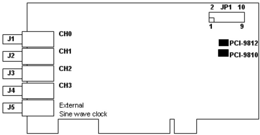
The PCI-9812/9810 connects to external devices via five BNC connectors and one 10-pin dual-in-line header. Figure 2-1 shows the location of these connectors.
![J1\nCH0\nJ2\nCH1\nJ3\nCH2\nJ4\nCH3\nJ5\nExternal\nSine wave clock\nPCI-9812\nPCI-9810\n2 JP1 10\n1 9](.pci-9812-9810-50-11116-2040-302/1d31b9c6c62cc6f7d47ab5bfb4b9ea53f2f194e287bc0de1b5383e9a6bace5f8.jpg)

Figure 2-1: Location of Connectors

<table><tr><td>J1</td><td>Input signal of channel 0 A/D converter.</td></tr><tr><td>J2</td><td>Input signal of channel 1 A/D converter.</td></tr><tr><td>J3</td><td>Input signal of channel 2 A/D converter.</td></tr><tr><td>J4</td><td>Input signal of channel 3 A/D converter.</td></tr><tr><td>J5</td><td>Input signal of external clock 0.</td></tr><tr><td>JP1</td><td>This 10-pin connector is for digital input signal, including a digital clock, a digital trigger, and three digital inputs.</td></tr></table>

# JP1 Pin Definition

Below is the default JP1 pin assignment.

<table><tr><td>Pin</td><td>Signal</td></tr><tr><td>1</td><td>External Clock Input 1</td></tr><tr><td>2</td><td>Ground</td></tr><tr><td>3</td><td>External Digital Trigger Input</td></tr><tr><td>4</td><td>Ground</td></tr><tr><td>5</td><td>Digital Input 0</td></tr><tr><td>6</td><td>Ground</td></tr><tr><td>7</td><td>Digital Input 1</td></tr><tr><td>8</td><td>Ground</td></tr><tr><td>9</td><td>Digital Input 2</td></tr><tr><td>10</td><td>Ground</td></tr></table>

Table 2-1: JP1 Pin Definition

When JP1 is connected to a 9-pin D-type connector using a ribbon cable, the pin-out of the D-type connector is changed to:

<table><tr><td>Pin</td><td>Signal</td></tr><tr><td>1</td><td>External Clock Input 1</td></tr><tr><td>2</td><td>Ground</td></tr><tr><td>3</td><td>External Digital Trigger Input</td></tr><tr><td>4</td><td>Ground</td></tr><tr><td>5</td><td>Digital Input 0</td></tr><tr><td>6</td><td>Ground</td></tr><tr><td>7</td><td>Digital Input 1</td></tr><tr><td>8</td><td>Ground</td></tr><tr><td>9</td><td>Digital Input 2</td></tr><tr><td>10</td><td>N/A</td></tr></table>

Table 2-2: JP1 Pin Definition Connected to 9-pin D-type Connector

# 2.3 Input Settings

This section describes the characteristics and settings of the PCI-9812/9810 inputs.

# Analog Input

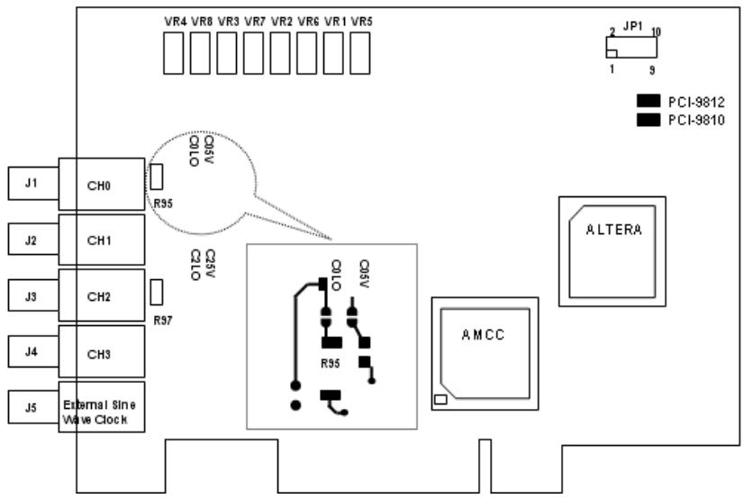
The PCI-9812/9810 has four analog input channels which are connected through the J1 to J4 connectors. The input impedance and input amplitude range can be changed through soldering the gap switches on the board (refer to PCI-9812/9810 layout). A solder gap switch consists of two copper pads. The switch can be turned on by soldering the copper pads. As all four channels use the same method to configure their input characteristics, only channel 0 is discussed here. There are two solder gap switches labeled as COLO (channel 0 low impedance) and C05V (channel 0 5 V input) to setup the input of channel 0. Refer to Figure 2-1.

<table><tr><td>C0LO</td><td>C05V</td><td>Input Impedance</td><td>Input Range</td></tr><tr><td>Open</td><td>Open</td><td>High (~15 MΩ)</td><td>±1 V</td></tr><tr><td>Open</td><td>Close</td><td>1.25 KΩ</td><td>±5 V</td></tr><tr><td>Close</td><td>Open</td><td>Low (50 Ω)</td><td>±1 V (default)</td></tr><tr><td>Close</td><td>Close</td><td>Low (50 Ω)</td><td>±5 V</td></tr></table>

Table 2-3: Analog Input

# CAUTION

![The image displays a yellow triangular warning sign with a thick black border. Inside the triangle is a black exclamation mark with a red dot at the bottom. A small strip of white background is visible on the top left, and a black area is visible on the top right.](.pci-9812-9810-50-11116-2040-302/d9855c8deaf25ff47224c7fdb9603970771829b5102a5ad7120ad820532f11ad.jpg)

DO NOT leave the input connector unconnected when it is configured as high impedance input. The input connector must be connected to a low impedance signal source to provide a return path for the input bias current. Since the OPAMP has a maximum input bias current of $35 \mu A$ in the input stage, it will be placed in an abnormal environment when the input is left unconnected and will lead to saturation in the output stage. Although a current-limiting resistor is present to protect the ADC, the large current brought by the saturation will damage the ADC.

Offset problems will occur if you use high impedance ( $\sim$ 15 M $\Omega$ ) with signal sources having high output impedance. The high output impedance and the input bias current of up to 35 $\mu$ A introduces a voltage drop of several volts. Adjusting the variable resistor does not eliminate this large offset voltage.

# NOTE

75 $\Omega$ input impedance can be achieved by: (1) replacing R95 with a 75-ohm resistor and close COLO or (2) placing a T-connector with a 75-ohm terminator on J1 and open COLO.

The corresponding switches and resistors of other channels are listed below:

<table><tr><td>Channel</td><td colspan="2">Switches</td><td>Resistor</td></tr><tr><td>Channel 0</td><td>C0LO</td><td>C05V</td><td>R95</td></tr><tr><td>Channel 1</td><td>C1LO</td><td>C15V</td><td>R96</td></tr><tr><td>Channel 2</td><td>C2LO</td><td>C25V</td><td>R97</td></tr><tr><td>Channel 3</td><td>C3LO</td><td>C35V</td><td>R98</td></tr></table>

Table 2-4: Switches and Resistors

# External Clock 0

The external clock 0 (J5) is a sine wave signal that is converted to a TTL signal inside the PCI-9812/9810. This signal is AC coupled. The input impedance of external clock 0 is $50\Omega$ and the input level is $2\mathrm{V}$ peak-to-peak.

Note that the external clock frequency is the system clock. The maximum A/D clock frequency is half of the system clock. When using the external sine clock for PCI-9812, take note that the frequency of the sine clock must be above 300 KHz. Otherwise the sine clock will be converted into a digital clock with a long rise time. When the rise time of a clock signal is too long, the CPLD may not work as specified and the real sample clock fed into the ADC will not be continuous. This explains why users will see a different sampled waveform when using a slower sine wave clock. If slower sampling rate is necessary when using PCI-9812/9810, you could feed a sine wave clock that has the frequency higher than 300 KHz, and use the clock divisor to obtain a slower sampling rate.

# External Clock 1

The external clock 1 (JP1 pin 1) is a digital clock. The input impedance is $50\Omega$ and the input level into the 50 ohm-load should be between 2.4 V and 5 V. This signal is DC coupled.

# Digital Input

The PCI-9812/9810 has four digital inputs: an external digital trigger (JP1 pin3) and three general-purpose digital inputs (JP1 pin 5, 7, and 9). These inputs are TTL-compatible with 10 KΩ pull-down resistors.

The PCI-9812/9810 also performs an automatic configuration of the IRQ and I/O port address. There is no need to set any configuration, as you would use in an ISA form factor DAQ card. For system reliability, it is necessary to manually assign some critical settings for analog input/output as these settings will not be changed after your data acquisition system configuration is decided. The software package cannot change this configuration when the system is running.

# 3 Installation

# 3.1 Before You Proceed

The PCI-9812/9810 card has electrostatic sensitive components that can be easily damaged by static electricity. The card must be handled on a grounded anti-static mat. The operator must wear an anti-static wristband, grounded at the same point as the anti-static mat.

Inspect the card module carton for damages. Shipping and handling could cause damage to the module. Make sure that the card has no damage before installing.

After opening the card packaging, get the module and place it on a grounded anti-static surface with component side up, then carefully inspect the module for any damage. Press down all socketed IC's to make sure that they are properly seated. Do this only with the module placed on a firm flat surface.

WARNING Do not attempt to install a damaged board into the computer.

# 3.2 Installing the Card

1. Turn off the system/chassis and disconnect the power plug from the power source.
2. Remove the system/chassis cover.
3. Select the PCI slot that you intend to use, then remove the bracket opposite the slot, if any. The selected slot must provide bus-mastering capability.
4. Align the card connectors (golden fingers) with the slot, then press the card firmly until the card is completely seated on the slot.
5. Secure the card to the chassis with a screw.
6. Replace the system/chassis cover.
7. Connect the power plug to a power source, then turn on the system/chassis.

# 3.3 Configuring the Card

As a plug and play component, the card requests an interrupt number through its PCI controller. The system BIOS responds with an interrupt assignment based on the card information and on known system parameters. These system parameters are determined by the installed drivers and the hardware load detected by the system.

# Troubleshooting

If your system fails to boot or if you experience erratic operation with your PCI board in place, this is likely caused by an interrupt conflict (i.e. the BIOS Setup is incorrectly configured). Refer to the BIOS documentation that came with the system for details.

# 3.4 Installing the Drivers for Windows

The Plug and Play function of Windows 95/98/2000 automatically detects the newly installed card. If this is the first time you installed the card in the system, you will be prompted to search for the device information source. Refer to the Software Installation Guide for instructions on how to install the device drivers.

# 4 Registers

Descriptions of the register format and structure of the PCI-9812/9810 are specified in this chapter. This information is for programmers that want to handle the card using low-level programming.

# 4.1 I/O Port Address

The PCI-9812/9810 functions as a 32-bit PCI target device to any master on the PCI bus. It supports burst transfer to memory space by using 32-bit data — where both data read and write are based on 32-bit data transfer. Table 4-1 lists the I/O address of each register according to the base address and the register function.

<table><tr><td>I/O Address</td><td>Read</td><td>Write</td></tr><tr><td>Base + 0</td><td>—</td><td>ADC Channel Enable Register</td></tr><tr><td>Base + 4</td><td>—</td><td>ADC Clock Divisor Register</td></tr><tr><td>Base + 8</td><td>—</td><td>Trigger Mode Register</td></tr><tr><td>Base + C</td><td>—</td><td>Trigger Level Register</td></tr><tr><td>Base + 10</td><td>—</td><td>Trigger Source Register</td></tr><tr><td>Base + 14</td><td>—</td><td>Post Trigger Counter Register</td></tr><tr><td>Base + 18</td><td>FIFO Control &amp; Status Reg</td><td>FIFO Control &amp; Status Register</td></tr><tr><td>Base + 1C</td><td>—</td><td>Acquisition Enable Register</td></tr><tr><td>Base + 20</td><td>—</td><td>Clock Source Register</td></tr></table>

Table 4-1: I/O Address

# ADC Channel Enable Register

The PCI-9812/9810 has four analog input channels: CH0, CH1, CH2, and CH3. CH0 to CH3 may be enabled or disabled by bit 0 to bit 3 of the ADC channel enable register.

Address: BASE + 0

Attribute: Write only

Data Format:

<table><tr><td>Bit</td><td>7</td><td>6</td><td>5</td><td>4</td><td>3</td><td>2</td><td>1</td><td>0</td></tr><tr><td>BASE+0</td><td>—</td><td>—</td><td>—</td><td>—</td><td>CH3EN</td><td>CH2EN</td><td>CH1EN</td><td>CH0EN</td></tr><tr><td>BASE+1</td><td>—</td><td>—</td><td>—</td><td>—</td><td>—</td><td>—</td><td>—</td><td>—</td></tr><tr><td>BASE+2</td><td>—</td><td>—</td><td>—</td><td>—</td><td>—</td><td>—</td><td>—</td><td>—</td></tr><tr><td>BASE+3</td><td>—</td><td>—</td><td>—</td><td>—</td><td>—</td><td>—</td><td>—</td><td>—</td></tr></table>

Bit 31->4 Any value

Bit 3 CH3EN

Bit 2 CH2EN

Bit 1 CH1EN

Bit 0 CH0EN

Allowed combinations (refer to section 5.5) of these bits include:

0000 No channel is enabled.

0001 Only CH0 is enabled.

0011 CH0 and CH1 are enabled.

1111 All channels are enabled.

# ADC Clock Divisor Register

Feeding the ADC source clock to a clock frequency divider generates the ADC sampling clock. The output of the frequency divider becomes the sampling clock. The frequency of the ADC sampling clock is:

Frequency of source clock / ADC clock divisor

Address: BASE+04h

Attribute: Write only

Data Format:

<table><tr><td>Bit</td><td>7</td><td>6</td><td>5</td><td>4</td><td>3</td><td>2</td><td>1</td><td>0</td></tr><tr><td>Base+4</td><td>DIV7</td><td>DIV6</td><td>DIV5</td><td>DIV4</td><td>DIV3</td><td>DIV2</td><td>DIV1</td><td>DIV0</td></tr><tr><td>Base+5</td><td>DIV15</td><td>DIV14</td><td>DIV13</td><td>DIV12</td><td>DIV11</td><td>DIV10</td><td>DIV9</td><td>DIV8</td></tr><tr><td>Base+6</td><td>—</td><td>—</td><td>—</td><td>—</td><td>—</td><td>—</td><td>—</td><td>—</td></tr><tr><td>Base+7</td><td>—</td><td>—</td><td>—</td><td>—</td><td>—</td><td>—</td><td>—</td><td>—</td></tr></table>

DIV15...0 AD clock frequency devisor.

— Any value

NOTE The minimum value of this register is 2, and the DIV0 is hardwired to 0.

# Trigger Mode Register

The PCI-9812/9810 has five trigger modes: software trigger, post trigger, pre-trigger, middle trigger and delay trigger. The trigger mode register is used to specify which trigger mode is currently used.

Address: BASE + 08h

Attribute: write only

Data Format:

<table><tr><td>Bit</td><td>7</td><td>6</td><td>5</td><td>4</td><td>3</td><td>2</td><td>1</td><td>0</td></tr><tr><td>Base + 8</td><td>—</td><td>—</td><td>—</td><td>—</td><td>—</td><td>TRGMOD2</td><td>TRGMOD1</td><td>TRGMOD0</td></tr><tr><td>Base + 9</td><td>—</td><td>—</td><td>—</td><td>—</td><td>—</td><td>—</td><td>—</td><td>—</td></tr><tr><td>Base + A</td><td>—</td><td>—</td><td>—</td><td>—</td><td>—</td><td>—</td><td>—</td><td>—</td></tr><tr><td>Base + B</td><td>—</td><td>—</td><td>—</td><td>—</td><td>—</td><td>—</td><td>—</td><td>—</td></tr></table>

TRGMOD2...0 Trigger mode. See trigger mode table below.

— Any value

<table><tr><td>TRGMOD2</td><td>TRGMOD1</td><td>TRGMOD0</td><td>Trigger Mode</td></tr><tr><td>0</td><td>0</td><td>0</td><td>Software trigger</td></tr><tr><td>0</td><td>0</td><td>1</td><td>Post trigger</td></tr><tr><td>0</td><td>1</td><td>0</td><td>Pre-trigger</td></tr><tr><td>0</td><td>1</td><td>1</td><td>Delay trigger</td></tr><tr><td>1</td><td>0</td><td>0</td><td>Middle trigger</td></tr></table>

Table 4-2: Five Trigger Modes

NOTE All other values for this register is not allowed. The card will fail to acquire data if you set an unsupported value to this register.

# Trigger Level Register

The trigger condition of the PCI-9812/9810 includes a trigger level and a trigger slope. This register sets the trigger level and the trigger source register described in the next section, and sets the trigger slope.

Address: BASE + 0ch

Attribute: Write only

Data Format:

<table><tr><td>Bit</td><td>7</td><td>6</td><td>5</td><td>4</td><td>3</td><td>2</td><td>1</td><td>0</td></tr><tr><td>BASE+Ch</td><td>TRGLVL7</td><td>TRGLVL6</td><td>TRGLVL5</td><td>TRGLVL4</td><td>TRGLVL3</td><td>TRGLVL2</td><td>TRGLVL1</td><td>TRGLVL0</td></tr><tr><td>BASE+Dh</td><td>—</td><td>—</td><td>—</td><td>—</td><td>—</td><td>—</td><td>—</td><td>—</td></tr><tr><td>BASE+Eh</td><td>—</td><td>—</td><td>—</td><td>—</td><td>—</td><td>—</td><td>—</td><td>—</td></tr><tr><td>BASE+Fh</td><td>—</td><td>—</td><td>—</td><td>—</td><td>—</td><td>—</td><td>—</td><td>—</td></tr></table>

TRGLVL7...0 Trigger level

— Any value

Relationship between the 8-bit trigger level and the trigger voltage:

<table><tr><td>TRGLVL7..0(bit 7..0)</td><td>Trigger voltage(±1 V)</td><td>Trigger voltage(±5 V)</td></tr><tr><td>0xFF</td><td>0.992 V</td><td>4.96 V</td></tr><tr><td>0xFE</td><td>0.984 V</td><td>4.92 V</td></tr><tr><td>|</td><td>|</td><td>|</td></tr><tr><td>0x81</td><td>0.008 V</td><td>0.04 V</td></tr><tr><td>0x80</td><td>0.000 V</td><td>0.00 V</td></tr><tr><td>0x7F</td><td>-0.008 V</td><td>-0.04 V</td></tr><tr><td>|</td><td>|</td><td>|</td></tr><tr><td>0x01</td><td>-0.992 V</td><td>-4.96 V</td></tr><tr><td>0x00</td><td>-1.000 V</td><td>-5.00 V</td></tr></table>

# Trigger Source Register

The PCI-9812/9810 supports five trigger sources: CH0, CH1, CH2, CH3, and external digital trigger.

Address: BASE + 10h

Attribute: Write only

Data Format:

<table><tr><td>Bit</td><td>7</td><td>6</td><td>5</td><td>4</td><td>3</td><td>2</td><td>1</td><td>0</td></tr><tr><td>Base + 10</td><td>--</td><td>--</td><td>--</td><td>--</td><td>TRGSLP</td><td>TRGSRC2</td><td>TRGSRC1</td><td>TRGSRC0</td></tr><tr><td>Base + 11</td><td>--</td><td>--</td><td>--</td><td>--</td><td>—</td><td>—</td><td>—</td><td>—</td></tr><tr><td>Base + 12</td><td>--</td><td>--</td><td>--</td><td>--</td><td>—</td><td>—</td><td>—</td><td>—</td></tr><tr><td>Base + 13</td><td>--</td><td>--</td><td>--</td><td>--</td><td>—</td><td>—</td><td>—</td><td>—</td></tr></table>

TRGSLP

Trigger slope

0: Positive slope trigger

1: Negative slope trigger

TRGSRC2 > TRGSRC0

Trigger source

<table><tr><td>TRIGSRC2</td><td>TRIGSRC2</td><td>TRIGSRC2</td><td>Trigger source</td></tr><tr><td>0</td><td>0</td><td>0</td><td>CH0</td></tr><tr><td>0</td><td>0</td><td>1</td><td>CH1</td></tr><tr><td>0</td><td>1</td><td>0</td><td>CH2</td></tr><tr><td>0</td><td>1</td><td>1</td><td>CH3</td></tr><tr><td>1</td><td>X</td><td>X</td><td>EX_DIG_trigger</td></tr></table>

When the external digital trigger is selected, the positive slope trigger equals to the rising edge trigger, the negative slope trigger equals to the falling edge trigger, and the value of trigger level register becomes meaningless.

# Post Trigger Counter Register

The post trigger counter is a 16-bit down counter. The counter is pre-loaded with the value in the post trigger counter register and will count down on the rising edge of ADC sampling clock after the trigger condition is met. When the count reaches 0, the counter stops. The counter is used to control the delay time in delay trigger mode and to control the post trigger sampling count in middle trigger mode.

Address: BASE + 14h

Attribute: write only

Data Format:

<table><tr><td>Bit</td><td>7</td><td>6</td><td>5</td><td>4</td><td>3</td><td>2</td><td>1</td><td>0</td></tr><tr><td>BASE+Ch</td><td>PSTCN 7</td><td>PSTCN 6</td><td>PSTCN 5</td><td>PSTCN 4</td><td>PSTCN 3</td><td>PSTCN 2</td><td>PSTCN 1</td><td>PSTCN0</td></tr><tr><td>BASE+Dh</td><td>PSTCN15</td><td>PSTCN14</td><td>PSTCN13</td><td>PSTCN12</td><td>PSTCN11</td><td>PSTCN10</td><td>PSTCN9</td><td>PSTCN8</td></tr><tr><td>BASE+Eh</td><td>—</td><td>—</td><td>—</td><td>—</td><td>—</td><td>—</td><td>—</td><td>—</td></tr><tr><td>BASE+Fh</td><td>—</td><td>—</td><td>—</td><td>—</td><td>—</td><td>—</td><td>—</td><td>—</td></tr></table>

PSTCNT15...0 This value is pre-loaded to the post trigger counter when the post trigger counter register is written.

— Any value

# FIFO Status Register

Monitors some of the PCI-9812/9810 status.

Address: BASE + 18h

Attribute: Read

Data Format:

<table><tr><td>Bit</td><td>7</td><td>6</td><td>5</td><td>4</td><td>3</td><td>2</td><td>1</td><td>0</td></tr><tr><td>BASE+18h</td><td>—</td><td>—</td><td>ACQ</td><td>TD</td><td>PTCO</td><td>FIFOOR</td><td>FIFOHF</td><td>FIFOIR</td></tr><tr><td>BASE+19h</td><td>—</td><td>—</td><td>—</td><td>—</td><td>—</td><td>—</td><td>—</td><td>—</td></tr><tr><td>BASE+1Ah</td><td>—</td><td>—</td><td>—</td><td>—</td><td>—</td><td>—</td><td>—</td><td>—</td></tr><tr><td>BASE+1Bh</td><td>—</td><td>—</td><td>—</td><td>—</td><td>—</td><td>—</td><td>—</td><td>—</td></tr></table>

Bit 0 FIFOIR, FIFO input ready flag.

0: FIFO is not ready for input; FIFO is full.

1: FIFO is ready for input (not full).

Bit 1 FIFOHF, FIFO half full flag.

0: FIFO is not half-full yet.

1: FIFO is at least half-full.

Bit 2 FIFOOR, FIFO output ready flag

0: FIFO is not ready for output; FIFO is empty.

1: FIFO is ready for output (not empty).

Bit 3 PTC0, post trigger counter is 0

0: Post trigger counter is not 0.

1: Post trigger counter reached 0.

Bit 4 TD, trigger detection flag

0: No trigger condition has been met; no trigger is detected.

1: Trigger is detected.

Bit 5 ACQ, acquisition flag

0: Card is not acquiring data. Card maybe disabled or is waiting for a trigger.

1: Card is acquiring data.

Bit 6..31 Any value

# FIFO Control Register

Controls the onboard FIFO memory.

Address: BASE + 18h

Attribute: Write

Data Format:

<table><tr><td>Bit</td><td>7</td><td>6</td><td>5</td><td>4</td><td>3</td><td>2</td><td>1</td><td>0</td></tr><tr><td>BASE+18h</td><td>—</td><td>—</td><td>—</td><td>—</td><td>—</td><td>—</td><td>CLRTRG</td><td>CLRFIFO</td></tr><tr><td>BASE+19h</td><td>—</td><td>—</td><td>—</td><td>—</td><td>—</td><td>—</td><td>—</td><td>—</td></tr><tr><td>BASE+1Ah</td><td>—</td><td>—</td><td>—</td><td>—</td><td>—</td><td>—</td><td>—</td><td>—</td></tr><tr><td>BASE+1Bh</td><td>—</td><td>—</td><td>—</td><td>—</td><td>—</td><td>—</td><td>—</td><td>—</td></tr></table>

Bit 0 CLRFIFO, clear the onboard FIFO

When a “1” is written to this bit, the entire onboard FIFO is cleared.

Bit 1 CLRTRG, clear trigger detection flag

When a “1” is written to this bit, the trigger detection bit is cleared.

Bit 2..31 Any value

# Acquisition Enable Register

Enables or disables the ADC acquisition.

Address: BASE + 1ch

Attribute: Write only

Data Format:

<table><tr><td>Bit</td><td>7</td><td>6</td><td>5</td><td>4</td><td>3</td><td>2</td><td>1</td><td>0</td></tr><tr><td>BASE+18h</td><td>—</td><td>—</td><td>—</td><td>—</td><td>—</td><td>—</td><td>—</td><td>ACQEN</td></tr><tr><td>BASE+19h</td><td>—</td><td>—</td><td>—</td><td>—</td><td>—</td><td>—</td><td>—</td><td>—</td></tr><tr><td>BASE+1Ah</td><td>—</td><td>—</td><td>—</td><td>—</td><td>—</td><td>—</td><td>—</td><td>—</td></tr><tr><td>BASE+1Bh</td><td>—</td><td>—</td><td>—</td><td>—</td><td>—</td><td>—</td><td>—</td><td>—</td></tr></table>

Bit 31...1 No value

Bit 0 ACQEN, acquisition enable

When a “1” is written to this bit, the PCI-9812/9810 is ready to sample data. When a “0” is written, the PCI-9812/9810 is disabled.

# Clock Source Register

Selects the system clock source.

Address: BASE + 20h

Attribute: Write only

Data Format:

<table><tr><td>Bit</td><td>7</td><td>6</td><td>5</td><td>4</td><td>3</td><td>2</td><td>1</td><td>0</td></tr><tr><td>BASE+18h</td><td>—</td><td>—</td><td>—</td><td>—</td><td>—</td><td>CLKSRC1</td><td>CLKSRC0</td><td>Freq_Sel</td></tr><tr><td>BASE+19h</td><td>—</td><td>—</td><td>—</td><td>—</td><td>—</td><td>—</td><td>—</td><td>—</td></tr><tr><td>BASE+1Ah</td><td>—</td><td>—</td><td>—</td><td>—</td><td>—</td><td>—</td><td>—</td><td>—</td></tr><tr><td>BASE+1Bh</td><td>—</td><td>—</td><td>—</td><td>—</td><td>—</td><td>—</td><td>—</td><td>—</td></tr></table>

Bit 31...3 Any value

Bit 2...1 CLKSRC1...0, ADC clock source

Bit 0 Freq\_Sel: Frequency selection. Values include:

1: Frequency of A/D clock source is higher than the PCI clock frequency (33 MHz)

0: Frequency of A/D clock source is lower than the PCI clock frequency (33 MHz)

<table><tr><td>CLKSRC2</td><td>CLKSRC1</td><td>Selected clock source</td></tr><tr><td>0</td><td>0</td><td>Internal clock (40 MHz)</td></tr><tr><td>0</td><td>1</td><td>External sine wave clock</td></tr><tr><td>1</td><td>0</td><td>External digital clock</td></tr><tr><td>1</td><td>1</td><td>Illegal</td></tr></table>

# NOTE

When selected, the external clock is divided by the frequency divider as mentioned. Thus, the frequency of the external clock should be at least twice as the desired sampling frequency.

# 4.2 High Level Programming

The PCI-9812/9810 card can be controlled directly using high-level Application Programming Interface (API) that bypasses the detailed register structures. The software libraries, including DOS for Borland C++ and DLL driver for Windows 95 are included in the ADLINK All-in-One CD. For further information, refer to Chapter 6.

# 4.3 Low Level Programming

You are not required to write any hardware dependent low-level programs to operate the PCI-9812/9810 card. Since this process is more complex and the relevant information are not described in this manual, ADLINK does not recommend low-level application programming. The PCI-9812 uses the AMCC-S5933 PCI controller. For more information on the s5933 PCI controller, visit www.amcc.com.

# 5 Operation Theory

The operation theorem of the PCI-9812/9810 card functions is described in this chapter. These functions include A/D conversion and digital input. This section aims to assist you in understanding, operating, and programming the PCI-9812/9810.

# 5.1 Conversion Procedure

Before programming the PCI-9812/9810 to perform A/D conversions, you must first understand the following concepts:

▶ A/D signal source control

When using an A/D converter, you must be familiar with the properties of the signal to be measured, and you must decide which channels to use and connect the signals to the PCI-9812/9810 card. In addition, you must define and control the A/D signal sources, including the A/D channels, A/D gains, and A/D signal types. Refer to section 5.2 for A/D signal source control.

▶ A/D trigger source control

After identifying the A/D signal source, you must decide how to trigger the A/D conversion and define or control the trigger source. The A/D converter will start to convert the signal to a digital value when a trigger condition is met. Refer to section 5.3.

▶ A/D clock control

The A/D clock is controlled by an internal or external clock source. The operation of the A/D clock source is described in section 5.4.

# ▶ A/D data transfer mode

In the end of an A/D conversion, the A/D data is buffered in a FIFO. The total FIFO size on PCI-9812/9810 is 32K samples. This buffer size is relative to the highest data transfer rate. The A/D data should be transferred to the computer's memory for further processing. The cards use DMA to transfer the A/D data to host memory. Refer to section 5.5.

# ▶ A/D data format

To process the A/D data, programmers must be familiar with the A/D data format. Refer to section 5.6.

# 5.2 Signal Source Control

To control the A/D signal source, the signal type, signal channel, and signal range must be determined.

# Signal Type

The A/D signal sources of PCI-9812/9810 are single-ended (SE).

# Channels

There are four channels for SE mode. The ADC Channel Enable Register controls the channel number. Refer to section 4.1.

# Signal Range and Input impedance

The proper signal range is important for data acquisition. The available signal input ranges for the PCI-9812/9810 are $\pm5$ V or $\pm1$ V, which are set by soldering the copper pads on the PCB. The input impedance for high-speed applications should also be considered. The selectable input impedance values are 50 $\Omega$ , 1.25 K, 15 M $\Omega$ . Refer to section 2.3 for details.

# 5.3 Trigger Source Control

When performing trigger acquisition in the PCI-9812/9810, the following parameters have to be specified before DMA operation starts:

▶ Clock source. Refer to section 5.4
▶ Clock rate. Refer to section 5.4
▶ Trigger sources. Refer to next section.
▶ Trigger level. The trigger event occurs when the trigger signal crosses the specified trigger voltage. Refer to Trigger Level Register section for the relationship between the 8-bit trigger level and the trigger voltage.

The trigger is detected while the trigger event occurs. For post-trigger and middle-trigger, the data acquisition is performed after the trigger event. However, the time that the AD conversion starts is 350 ns slower than the trigger detection time. This 350 ns delay has some minor effect to high-speed data acquisition.

▶ Trigger polarity. Trigger slope with a 0 value indicates a positive trigger while a 1 value indicates a negative trigger.

# Trigger Sources

▶ Internal trigger

This is a software trigger. The trigger event occurs when you call \_9812\_AD\_DMA\_Start() function to start the operation.

▶ External analog trigger

You can use the signal on any analog input channel (CH0, CH1, CH2, or CH3) as the trigger signal for external analog trigger. Below are two conditions for analog triggers.

▷ Positive-slope trigger

The trigger event occurs the first time the trigger signal (analog input signal) changes from a voltage that is lower than the specified trigger level to a voltage that is higher than the specified trigger level.

▷ Negative-slope trigger

The trigger event occurs the first time the trigger signal (analog input signal) changes from a voltage that is higher than the specified trigger level to a voltage that is lower than the specified trigger level.

![| Level         | Event Description                     |\n| ------------- | ------------------------------------- |\n| +0.5V         | Negative-slope trigger event occurs    |](.pci-9812-9810-50-11116-2040-302/92562c5613ddec463d3378bfa361316441fda6550b83ac7437402c4d312f1c1d.jpg)

▷ External Digital Trigger

An external digital trigger occurs when a rising edge or a falling edge is detected on the digital signal connected to pin3 of JP1 for external digital trigger.

![Positive-edge trigger\nevent occurs\nNegative-edge\ntrigger event occurs](.pci-9812-9810-50-11116-2040-302/53dc76bd23f29ce66c664e8068acc9986839c7444bca64f9fd5f795e41231583.jpg)

▶ Simultaneous trigger for multiple cards

When multiple PCI-9812/9810 cards are installed in a single system, the trigger sources of each card may be connected together to achieve simultaneous trigger. Note that simultaneous trigger is not equivalent to simultaneous A/D conversion. The theoretical time difference between the samples on two different cards will be $\frac{1}{2}$ of the clock period. Refer to section 5.4 for more information on A/D conversion clock control.

# Trigger Modes

# ▶ Software-trigger acquisition

This trigger mode does not require any external trigger source. The trigger event occurs when the \_9812\_AD\_DMA\_Start() function is called to start the operation.

# ▶ Post-trigger acquisition

Use post-trigger for applications where data needs to be collected after a specified trigger event. The trigger can either be an external analog trigger or digital trigger.

![Based on the provided image, here is the accurate description of the flowchart:\n\n**Labeled Blocks (Text):**\n*   DMA start\n*   External trigger Event\n*   Acquire N A/D data after trigger event\n*   DMA stop\n*   Time\n*   Acquisition Start\n\n**Connections and Structure:**\nThe diagram is organized around a horizontal blue line representing a timeline, which ends with an arrowhead pointing to the right labeled 'Time'.\n\n*   **DMA start:** A blue arrow points downward from this text to the timeline on the far left.\n*   **External trigger Event / Acquisition Start:** In the center of the timeline, a blue arrow points downward from 'External trigger Event'. Directly below this same point on the timeline, another blue arrow points upward from a bracket labeled 'Acquisition Start'.\n*   **Acquire N A/D data after trigger event:** This text floats above the timeline between the trigger event and the stop event, describing the action taking place during that interval.\n*   **DMA stop:** A blue arrow points downward from this text to the timeline on the right.](.pci-9812-9810-50-11116-2040-302/eb4e26ff2fd5533d9eb202da1ff08e3d50ba3cfa6acc667a8c6ead37db0f2b62.jpg)

Figure 5-1: Post-trigger Acquisition

# ▶ Pre-trigger acquisition

Use pre-trigger to collect data before a specified trigger event. The trigger can either be an external analog trigger or digital trigger. Data acquisition starts when DMA operation starts. The operation stops when the external trigger event occurs. If the external trigger occurs before the specified count of data is read (Specified by the \_9812\_AD\_DMA\_Start() function. Refer to section 6.2), the amount of retrieved data would be less than the specified count. However, if the external trigger occurs after the specified count of data is read, the application only samples the specified count of data.

![This diagram depicts a timeline of events flowing from left to right.\n\n**Central Element:**\n*   A horizontal blue line extending to the right, ending with an arrowhead and the label **'Time'**.\n\n**Events and Connections:**\n1.  **'DMA start'**: An arrow points downward to the timeline on the far left.\n2.  **'Acquire A/D data before trigger event'**: Text positioned above the timeline, situated between the start and trigger points.\n3.  **'External trigger Event'**: An arrow points downward to the timeline at a specific point to the right of the start.\n4.  **'Acquisition Stop'**: An arrow points upward to the timeline at the exact same location as the 'External trigger Event'.](.pci-9812-9810-50-11116-2040-302/fecc1fb51a2673551d561a510c01049d854673d5c0374738e50e73deb253eee0.jpg)

Figure 5-2: Pre-trigger Acquisition

# ▶ Middle-trigger acquisition

Use middle-trigger acquisition to collect data before and after a specified trigger event. The amount of data acquired before a trigger event occurs when using middle trigger may not equal to the specified count of data, just like the pre-trigger mode.

![The image displays a horizontal timeline labeled 'Time' at the bottom right. Three vertical arrows point downward from text labels to this timeline, marking specific points:\n\n1.  **DMA start**: The leftmost arrow points to the beginning of the timeline.\n2.  **External trigger Event**: The middle arrow points to a section further along the timeline.\n3.  **DMA Stop**: The rightmost arrow points to the end of the timeline.\n\nBetween these markers, text describes data acquisition phases:\n*   Between 'DMA start' and 'External trigger Event': **'Acquire m A/D data before trigger event'**\n*   Between 'External trigger Event' and 'DMA Stop': **'Acquire n A/D data after trigger event'**](.pci-9812-9810-50-11116-2040-302/b5fb3f3d07a086cfc0dcad6368f4647844aca4417465997ce3d795db63ca3086.jpg)

Figure 5-3: Middle-trigger Acquisition

The desired number of samples after trigger event is pre-loaded in post trigger counter register and will count down on the rising edge of ADC sampling clock after the trigger condition is met. When the count reaches 0, the counter stops. The trigger can either be an external analog trigger or digital trigger.

# ▶ Delay-trigger acquisition

Use delay trigger acquisition to delay the data collection after the specified trigger event occurs. The delay time is controlled by the value that is pre-loaded in the post trigger counter register. The counter then counts down on the rising edge of ADC sampling clock after the trigger condition was met.

When the count reaches 0, the counter stops and PCI-9812/9810 starts to acquire data.

![Based on the provided image, here is the description of the flowchart/timeline:\n\n**Labeled Blocks and Text:**\n*   'External trigger Event'\n*   'Post trigger counter count from N down to 0'\n*   'Acquisition start'\n*   'Acquire n A/D data'\n*   'DMA Stop'\n*   'Time'\n\n**Connections and Flow:**\nThe diagram displays a horizontal timeline running from left to right.\n1.  **Start:** A blue vertical arrow points downward from the text '**External trigger Event**' to the timeline.\n2.  **First Interval:** Between the first arrow and the second arrow, the text '**Post trigger counter count from N down to 0**' is centered above the timeline.\n3.  **Second Event:** A blue vertical arrow points downward from the text '**Acquisition start**' to the timeline.\n4.  **Second Interval:** Between the second arrow and the third arrow, the text '**Acquire n A/D data**' is centered above the timeline.\n5.  **Final Event:** A blue vertical arrow points downward from the text '**DMA Stop**' to the timeline.\n6.  **End:** The timeline concludes on the far right with the label '**Time**'.](.pci-9812-9810-50-11116-2040-302/5346f2fb1461f39224342e4ee34eb92c56aa8d4358c0488f2c18444667736b04.jpg)

Figure 5-4: Delay-trigger Acquisition

# 5.4 Clock Source Control

The AD clock source determines how the board regulates the timing of conversions when acquiring multiple samples from a single-channel or from a group of multiple channels. The A/D clock sources on the PCI-9812/9810 must use a pacer clock, but not single-shot as the A/D converters are in a pipelined structure, that require eight conversion clocks to complete the conversion of digital data.

# A/D Clock Sources

The A/D converters operate under the paced mode, which uses pacer clock for A/D conversion at a fixed rate. PCI-9812/9810 supports three clock sources for analog input conversion

# ▶ Internal Pacer Clock (default)

An onboard timer/counter is used as the internal A/D pacer clock. The frequency of the pacer is software-controllable. The maximum pacer signal rate is 40 MHz / 2 = 20 MHz, which is also the maximum sampling rate of PCI-9812/9810. Note that 40 MHz is the onboard clock. Feeding the clock source into a frequency divider generates the ADC sampling frequency. The following formula determines the ADC sampling frequency:

Sampling Rate = Frequency of Source Clock / ADC
Clock Divisor

NOTE The ADC Clock Divisor must be 2, 4, 6, 8,...65534 (max).

# ▶ External Pacer Clock

You can connect an external pacer clock to the EXTCLK1 (pin 1) on JP1 (for square wave) or Ext. Sine wave clock (for sine wave). Since you can handle the external signal with outside devices, the conversion rate of this mode is more flexible than the previous mode. When the external clock is selected, the frequency divider as mentioned also divides this external clock. Therefore the frequency of the external clock should be at least twice the sampling frequency. The formula is shown below:

Sampling Rate = Frequency of Source Clock / ADC
Clock Divisor

# NOTE

The clock divider must be an even number (2, 4, 6, 8, 10... 65534), with the minimum divider value being 2. Refer to section 6.2 to set the clock source and frequency divider.

The first AD sample takes several clocks to convert because of the ADC's pipelined architecture. Therefore, the external clock must be continuous for correct AD operation.

# ▶ Multiple cards operation

When multiple cards are installed in a single system, 4-channels on one card can achieve simultaneous conversion since they have the same internal clock source. However, the channels between two cards cannot be synchronized because the clock sources on different cards come from different sources. Even when the same external clock source is applied to all cards, the A/D conversion time is still possibly asynchronous because an onboard clock divider (divisible by 2) is used. Therefore, when the same external clock source is applied to multiple cards, the time difference of the sampling clocks between two cards will be half of the sampling clock period. The A/D clock cannot synchronize multiple cards.

# 5.5 Data Transfer

# Data Transfer

There are several function blocks on the PCI-9812/9810 designed to acquire AD data. Even as the maximum sampling rate is specified at up to 20 MHz, there are certain limitations due to the high total data throughput. Refer to the data transfer diagram below to understand how analog signal is converted to digital form and transferred to the host computer's memory. The data transfer rate limitation and bottleneck are discussed in this section.

![This flowchart illustrates a data acquisition and transfer path from analog-to-digital converters (ADCs) to a PCI bus.\n\n**Labeled Blocks:**\n*   **Inputs:** Four blocks labeled `ADC 0`, `ADC 1`, `ADC 2`, and `ADC 3`.\n*   **Intermediate Stage:** Four blocks labeled `Tristate latch`.\n*   **Buffer Stage:** Two blocks labeled `16K Samples FIFO`.\n*   **Controller:** One block labeled `PCI Controller`.\n*   **Output:** A label `PCI Bus` next to a double vertical line.\n\n**Connections:**\n*   **ADC to Latch:**\n    *   `ADC 0` output splits into two arrows, connecting to the top and second `Tristate latch` blocks.\n    *   `ADC 1` and `ADC 2` outputs connect to the third `Tristate latch` block.\n    *   `ADC 3` output connects to the fourth `Tristate latch` block.\n*   **Latch to FIFO:**\n    *   The top `Tristate latch` and the third `Tristate latch` connect to the top `16K Samples FIFO`.\n    *   The second `Tristate latch` and the fourth `Tristate latch` connect to the bottom `16K Samples FIFO`.\n*   **FIFO to Controller:** Both `16K Samples FIFO` blocks connect to the `PCI Controller`.\n*   **Controller to Bus:** The `PCI Controller` connects to the `PCI Bus`.](.pci-9812-9810-50-11116-2040-302/5e45b11c12cf3897787f4ec5f92a5ea10c93fca0076cd1ce9dfadf86ec2c44a9.jpg)

Figure 5-5: Data Transfer Diagram of PCI-9812/9810

# Simultaneous Sampling of Four AD Channels

The PCI-9812/9810 is equipped with four AD converters that support a maximum 20 MHz simultaneous sampling rate.

For single-channel applications, only channel 0 can be selected with a total FIFO length of 32K samples. For simultaneous two-channel applications, use channel 0 and channel 1 to optimize FIFO usage. The onboard circuit does not allow use of channel 0 and 2 or channel 2 and 3 simultaneously. Take note that the card only supports 2 or 4 channels for simultaneous sampling applications.

# Total Data Throughput

When four channels start simultaneously, the total data throughput from the AD converter to the onboard FIFO memory is:

Sampling Rate x number of channels x 2 bytes/channel

Therefore, the maximum total data throughput is 160 Mbytes/sec.

160MB/s = 20MHz x 4 channels x 2 bytes/channel

This extremely high data rate is beyond the 32-bit/33 MHz PCI bus bandwidth. To address this two 16K words (samples) FIFO are designed to buffer the data.

A total of 32K word (32K samples) is used when FIFO is onboard. When four channels are used, the FIFO size is 8K samples per channel. When two channels (#0 and #1) are used, the FIFO size is 16K samples per channel. When only one (#0) is used, the FIFO size is 32K samples.

You need to calculate the total data throughput for your applications, as this value would be relative to the total data length that can be continuously acquired.

# Maximum Acquiring Data Length

The burst PCI bandwidth is 132 MB/s. However, the effective sustained data rate is usually less than 100 MB/s. This value may even be lower when additional PCI devices are used simultaneously. If the total AD data throughput is lower than the PCI bandwidth, the AD data can be stored into the host memory through bus-mastering DMA and the total acquiring data length could be up to 64 MB (32M samples) which is the PCI controller's maximum. If the total AD data throughput is higher than the PCI bandwidth, the maximum data length will either be 16K or 8K samples, which is the maximum length from the size of onboard FIFO.

# Bus-mastering Data Transfer

PCI bus-mastering DMA is necessary for high speed DAQ in order to utilize the maximum PCI bandwidth. The bus-mastering controller—built into the AMCC-5933 PCI controller ASIC—controls the PCI bus when it becomes the master of the bus. Bus-mastering reduces the size of onboard memory and CPU loading since data is directly transferred to the computer's memory without CPU intervention.

The bus-mastering DMA provides the fastest data transfer rate on the PCI bus. Once the analog input operation starts, control returns to your program. The hardware temporarily stores the acquired data into the onboard A/D FIFO and transfers the data to a user-defined DMA buffer memory in the computer.

# NOTE

Even when the acquired data length is less than the FIFO, the AD data is directly transferred to the host memory by bus-mastering DMA.

As DMA transfer mode is very complex to program, ADLINK recommends using a high-level program library to control the card. If you want to apply a software that can handle the DMA bus master data transfer, visit www.amcc.com for more information on the PCI controller.

# Host Memory Operation

The DMA data transfer does not allow processing of AD data simultaneously with the data transfer. You must process the AD data after the completion of one DMA cycle. If the total data throughput in your application is relatively high (>20 MB/s), the processing time of AD data and the CPU computation power consumption must be considered. For example, if the CPU can only process data at a rate of 10 MB/s and you want to continuously acquire data at the rate of 20 MB/s; the FIFO eventually becomes full and data acquisition becomes discontinuous.

Storing data from the host memory to a hard disk or other storage devices must also be considered. The burst data rate of current HDD technology could be between 90 and 80 MB/s. However in reality, the effective bandwidth of a HDD is usually less than 10 MB/s, especially when the HDD seek time is longer. For example, if the HDD seek time is 20 ms, the FIFO is already full and the acquired data cannot be continuous.

Several limitations may be due to the OS and host memory size. In DOS, the maximum allocated memory size is less than 640K, except when you use an extended memory managing software. In Windows 95 or Windows NT, it is relatively difficult to get a continuously large memory size such as 64 MB. It is possible to allocate a large memory size by keeping the memory clean. The PCI bus-mastering DMA controller of the PCI-9812 needs continuous memory to store the AD data.

# 5.6 Data Format

The A/D data of 12-bit PCI-9812 is on the 12 MSB of the 16-bit A/D data. The 4 LSB of the 16-bit A/D data must be truncated by software (Refer to section 6.2). The relationship between the real signal voltage and the sampled value is shown below:

<table><tr><td>A/D Data (Hex)</td><td>Decimal Value</td><td>V (-1 V to +1 V)</td><td>V (-5 V to +5 V)</td></tr><tr><td>7FF 0</td><td>+32752</td><td>+1.0000</td><td>+5.0000</td></tr><tr><td>400 0</td><td>+16384</td><td>+0.5002</td><td>+2.5010</td></tr><tr><td>001 0</td><td>+16</td><td>+0.0005</td><td>+0.0025</td></tr><tr><td>000 0</td><td>0</td><td>0.0000</td><td>0.0000</td></tr><tr><td>FFF 0</td><td>-16</td><td>0.0005</td><td>-0.0025</td></tr><tr><td>C00 0</td><td>-16384</td><td>-0.5002</td><td>-2.5010</td></tr><tr><td>801 0</td><td>-32752</td><td>-1.0000</td><td>-5.0000</td></tr><tr><td>800 0</td><td>-32768</td><td>-1.0049</td><td>-5.0024</td></tr></table>

The A/D data of 10-bit PCI-9810 is on the 10 MSB of the A/D data. The 6 LSB of the 16-bit A/D data must be truncated by software. The relationship between the real signal voltage and the sampled value is shown below:

<table><tr><td>A/D Data (Hex)</td><td>Decimal Value</td><td>V (-1 V to +1 V)</td><td>V (-5 V to +5 V)</td></tr><tr><td>7FC 0</td><td>+32704</td><td>+1.0000</td><td>+5.0000</td></tr><tr><td>400 0</td><td>+16384</td><td>+0.5002</td><td>+2.5010</td></tr><tr><td>0040</td><td>+64</td><td>+0.0005</td><td>+0.0025</td></tr><tr><td>000 0</td><td>0</td><td>0.0000</td><td>0.0000</td></tr><tr><td>FFC 0</td><td>-64</td><td>-0.0005</td><td>-0.0025</td></tr><tr><td>C00 0</td><td>-16384</td><td>-0.5002</td><td>-2.5010</td></tr><tr><td>804 0</td><td>-32704</td><td>-1.0000</td><td>-5.0000</td></tr><tr><td>800 0</td><td>-32768</td><td>-1.0020</td><td>-5.0098</td></tr></table>

The formula showing the relationship of the A/D data and the analog value is:

$$
\text { Voltage } = \text { AD\_data } x (1 / K) x (\text { Gain })
$$

Where Gain and K are constants.

For analog input range -1 V to 1 V, Gain=1

For analog input range -5 V to 5 V, Gain=5.

For PCI-9812, K=2047×16=32752

For PCI-9810, K=511×64=32704.

# 6 Function Reference

This chapter describes the software library for operating the PCI-9812/9810 card. Only the functions for DOS and Windows 95 DLL are described. Refer to the PCIS-DASK function reference manual in the ADLINK All-in-One CD for descriptions of DLL functions for Windows 98/NT/2000.

The function prototypes and some useful constants are defined in the header files LIB directory (DOS) and INCLUDE directory (Windows 95). For Windows 95 DLL, the developing environment can be Visual Basic 4.0 or higher, Visual C/C++ 4.0 or higher, Borland C++ 5.0 or higher, Borland Delphi 2.x (32-bit) or higher, or any Windows programming language that allows calls to a DLL.

# 6.1 Installing the Libraries

Refer to the Software Installation Guide for more information on how to install the software libraries for DOS, Windows 95 DLL, or PCIS-DASK for Windows 98/NT/2000.

The device drivers and DLL functions of Windows 98/NT/2000 are included in the PCIS-DASK. Refer to the PCIS-DASK user's guide and function reference in the ADLINK All-in-One CD for programming information.

# 6.2 Programming Guide

# Naming Convention

The functions of NuDAQ and NuIPC PCI/CompactPCI cards' software driver use the following naming convention rules:

In DOS:

```jinja
_{hardware_model}_{action_name}
```

For example:

```cmake
_9812_Initial()
```

All functions in the PCI-9812 driver uses 9812 as {hardware\_model}. However, these may also be used by PCI-9810.

To differentiate the DOS from Windows 95 libraries, a capital W is placed in the beginning of each function name for Windows 95 DLL driver.

For example:

```txt
W_9812_Initial()
```

# Data Types

Some data types were defined in Pci\_9812.h (DOS) and Acl\_pci.h (Windows 95). These data types are used by the NuDAQ card library. It is recommended that you use these data types for your application programs. The following table lists the data type names and their ranges.

<table><tr><td>Type Name</td><td>Description</td><td>Range</td></tr><tr><td>U8</td><td>8-bit ASCII character</td><td>0 to 255</td></tr><tr><td>I16</td><td>16-bit signed integer</td><td>-32768 to 32767</td></tr><tr><td>U16</td><td>16-bit unsigned integer</td><td>0 to 65535</td></tr><tr><td>I32</td><td>32-bit signed integer</td><td>-2147483648 to 2147483647</td></tr><tr><td>U32</td><td>32-bit single-precision floating-point</td><td>0 to 4294967295</td></tr><tr><td>F32</td><td>32-bit single-precision floating-point</td><td>-3.402823E38 to 3.402823E38</td></tr><tr><td>F64</td><td>64-bit double-precision floating-point</td><td>-1.797683134862315E308 to 1.797683134862315E309</td></tr><tr><td>Boolean</td><td>Boolean logic value</td><td>TRUE, FALSE</td></tr></table>

Table 6-1: Data Types

# 6.3 Function Reference

# \_9812\_Initial

# Description

Initializes the PCI-9812/9810 card. Each PCI-9812/9810 card has to be initialized by this function before calling other functions.

# Syntax

```txt
C/C++ (DOS)
int _9812_Initial (int card_number, U16
*op_base_address, U16 *pt_base_address, U16
*irq_no, U16 *pci_master)

C/C++ (Windows 95)
int W_9812_Initial (int card_number, U16
*op_base_address, U16 *pt_base_address, U16
*irq_no, U16 *pci_master)
```

# Visual Basic (Windows 95)

```txt
W_9812_Initial (ByVal card_number As Long, op_base_address As Integer, pt_base_address As Integer, irq_no As Integer, pci_master As Integer) As Long
```

# Argument(s)

card\_number Card number of the card to be initialized. Valid card numbers are from 0 to 9.

op\_base\_address

Physical location of S5933 operation registers in the I/O space.

pt\_base\_address

Physical location of add-on registers in the pass-through I/O space.

irq\_no Interrupt IRQ level of the PCI-9812/9810 card. IRQ value is automatically assigned by the system BIOS.

pci\_master Tells whether the BIOS enabled or disabled bus mastering in the PCI Command Register.

# Return Code(s)

PCICardNumErr

PCIBiosNotExist

PCIBaseAddrErr

NoError

# \_9812\_Close

# Description

Closes a previously initialized 9812/9810 card.

# Syntax

$$
\mathrm{C} / \mathrm{C} + + (\mathrm{DOS})
$$

int \_9812\_Close (int card\_number)

$$
\mathrm{C} / \mathrm{C} + + (\text {   Windows   95   })
$$

int W\_9812\_Close (int card\_number)

Visual Basic (Windows 95)

W\_9812\_Close (ByVal card\_number As Long) As Long

# Argument(s)

card\_number Card number of the card to be initialized. Valid card numbers are from 0 to 9.

# Return Code(s)

PCICardNumErr

PCICardNotInit

NoError

# \_9812\_AD\_DMA\_Start

# Description

Starts an operation of A/D conversion N times with DMA data transfer. It will take place in the background, which will not stop until the Nth conversion has been completed or until your program executes \_9182\_AD\_DMA\_Stop to stop the operation. After executing this function, check the status of the operation by using the \_9812\_AD\_DMA\_Status function.

# Syntax

```txt
C/C++ (DOS)
```

```txt
int _9812_AD_DMA_Start (int card_number, int ch_cnt, U32 *buff, U32 count)
```

```txt
C/C++ (Windows 95)
```

```c
int W_9812_AD_DMA_Start(int card_number, int ch_cnt, HANDLE memID, U32 count)
```
Visual Basic (Windows 95)

```txt
W_9812_AD_DMA_Start (ByVal card_number As Long, ByVal ch_cnt As Long, ByVal handle As Long, ByVal count As Long) As Long
```

# Argument(s)

card\_number Card number of the selected card.
```txt
ch_cnt Number of A/D channel enabled. Valid values:
```

0 No channel is enabled.
1 Only channel 0 is enabled.
2 Channel 0 and 1 are enabled, and the sequence of channel scan is 0, 1, 0, 1, ...
4 All channels are enabled and the sequence of channel scan is 0, 1, 2, 3, 0, 1, 2, 3, ...

# buff (DOS)

Start address of the memory buffer that stores the A/D data. The buffer size must be larger than the number of A/D conversions. This memory should be in double-word alignment. The resolution of A/D data is 12-bit for PCI-9812 and 10-bit for PCI-9810. Refer to section 5.6 for the A/D data format.

The buffer format is:

<table><tr><td>DATA 1</td><td>DATA 2</td><td>DATA 3</td><td>DATA 4</td><td>......</td><td>DATA N-1</td><td>DATA N</td></tr><tr><td>16-bit</td><td>16-bit</td><td>16-bit</td><td>16-bit</td><td>16-bit</td><td>16-bit</td><td>16-bit</td></tr></table>

Each 16-bit data:

D11 D10 D9 ... D1 D0 b3 b2 b1 b0

where:

D11, D10, ..., D0: A/D converted data (9812) or

D11, D10, ..., D2: A/D converted data (9810).

b2, b1, b0: Digital input data from channel DI2, DI1, DI0.

b3: Trigger detection flag. Valid values:

0 No trigger is detected.

1 Trigger is detected.

memID (Win-95)

Memory ID of the allocated system DMA memory. In Windows 95, before calling W\_9812\_AD\_DMA\_Start, W\_9812\_Aloc\_DMA\_Mem must be called to allocate a contiguous DMA memory.

W\_9812\_Alloc\_DMA\_Mem returns a memory ID for identifying the allocated DMA memory and the linear address of the DMA memory to access the data. The format of the A/D data is the same as the DOS buffer (buff).

count Number of A/D conversion.

# Return Code(s)

PCICardNumErr
PCICardNotInit
InvalidDMACnt
BufNotDWordAlign
DMATransferNotAllowed
NoError

# \_9812\_AD\_DMA\_Status

# Description

Since \_9812\_AD\_DMA\_Start is executed in the background, the function \_9812\_AD\_DMA\_Status can be used to check its operation status.

# Syntax

```txt
C/C++ (DOS)
```

```c
int _9812_AD_DMA_Status(int card_number, int *count, int *status, U32 *start_idx)
```

```txt
C/C++ (Windows 95)
```

```c
int W_9812_AD_DMA_Status(int card_number, int *count, int *status, U32 *start_idx)
```

Visual Basic (Windows 95)

```txt
W_9812_AD_DMA_Status (ByVal card_number As Long, count As Long, status As Long, start_idx As Long) As Long
```

# Argument(s)

card\_number Card number of the selected card.

count Current amount of DMA transferred data.

status DMA data transfer status. Valid values:

0 DMA\_done
1 DMA\_continue
2 DMA\_wait\_trig
3 DMA\_wait\_delay

start\_idx The index where the data starts from is in the user's buffer. For example, the sequence of read data is:

```txt
buff[start_idx], buff[start_idx+1], _, buff[0], buff[1],_, .,buff[start_idx-1].
```

Return Code(s)

```txt
PCICardNumErr
PCICardNotInit
NoError
```

# \_9812\_AD\_DMA\_Stop

# Description

Stops the DMA data transfer. After executing this function, the \_9812\_AD\_DMA\_Start function stops. The function returns the number of transferred data, whether the A/D DMA data transfer is stopped by this function or by the DMA terminal count ISR.

# Syntax

```txt
C/C++ (DOS)
```

```c
int _9812_AD_DMA_Stop(int card_number, U32 *count)
```

```txt
C/C++ (Windows 95)
```

```c
int W_9812_AD_DMA_Stop(int card_number, U32 *count)
```

Visual Basic (Windows 95)

```txt
W_9812_AD_DMA_Stop (ByVal card_number As Long, count As Long) As Long
```

# Argument(s)

card\_number Card number of the selected card.

count Amount of transferred A/D data.

# Return Code(s)

```txt
PCICardNumErr
PCICardNotInit
NoError
```

# \_9812\_Set\_Clk\_Src

# Description

Specifies the ADC clock source.

# Syntax

```txt
C/C++ (DOS)
```

```txt
int _9812_Set_Clk_Src (int card_number, int clk_src, int ftpci)
```

```txt
C/C++ (Windows 95)
```

```c
int W_9812_Set_Clk_Src (int card_number, int clk_src, int ftpci)
```

Visual Basic (Windows 95)

```txt
W_9812_Set_Clk_Src (ByVal card_number As Long, ByVal clk_src As Long, ByVal ftpci As Long) As Long
```

# Argument(s)

card\_number The card number of PCI-9812/9810 to be selected

clk\_src The ADC clock source, the valid values are as follows:

0 INT\_CLK: internal clock
1 SIN\_CLK: external sin wave clock
2 SQR\_CLK: external square clock

ftpci Frequency selection.

AD2\_GT\_PCI The frequency of A/D clock source is higher than PCI clock frequency.

AD2\_LT\_PCI The frequency of A/D clock source is lower than PCI clock frequency.

# Return Code(s)

PCICardNumErr

PCICardNotInit

InvalidClkSrc

NoError

# \_9812\_Set\_Clk\_Rate

# Description

Specifies the clock divider for the ADC clock. The value of the clock divider must be even and between 2 to 65534.

# Syntax

```txt
C/C++ (DOS)
```

```txt
int _9812_Set_Clk_Rate (int card_number, U16 clk_div)
```

```txt
C/C++ (Windows 95)
```

```txt
int W_9812_Set_Clk_Rate (int card_number, U16 clk_div)
```

Visual Basic (Windows 95)

```txt
W_9812_Set_Clk_Rate (ByVal card_number As Long, ByVal clk_div As Integer) As Long
```

# Argument(s)

card\_number The card number of the selected card.

clk\_div ADC clock divisor. The value must be an even number and the minimum value is 2.

# Return Code(s)

```txt
PCICardNumErr
PCICardNotInit
InvalidClkDiv, NoError
```

# \_9812\_Set\_Trig

# Description

Sets up the trigger. The function specifies the trigger mode, trigger level (voltage), trigger source, trigger slope, and post trigger count. Refer to Chapter 5 for details.

# Syntax

```txt
C/C++ (DOS)
```

```c
int _9812_Set_Trig (int card_number, int trig_mode, int trig_src, int trig_pol, int trig_lvl, U16 post_trig_cnt)
```

```txt
C/C++ (Windows 95)
```

```c
int W_9812_Set_Trig (int card_number, int trig_mode, int trig_src, int trig_pol, int trig_lvl, U16 post_trig_cnt)
```
Visual Basic (Windows 95)

```txt
W_9812_Set_Trig (ByVal card_number As Long, ByVal trig_mode As Long, ByVal trig_src As Long, ByVal trig_pol As Long, ByVal trig_lvl As Long, ByVal post_trig_cnt As Integer) As Long
```

# Argument(s)

```txt
card_number Card number of the selected card.
```
trig\_mode Selected trigger mode. Valid values:

```txt
SOFT_TRIG    Software trigger
POST_TRIG    Post trigger
PRE_TRIG    Pre-trigger
DLY_TRIG    Delay trigger
MID_TRIG    Middle trigger
```
trig\_src Selected trigger source, the valid trigger sources are:

```csv
CH0_TRIG Channel 0
CH1_TRIG Channel 1
CH2_TRIG Channel 2
CH3_TRIG Channel 3
```

AUX\_TRIG

External digital trigger

trig\_pol

Trigger slope.

0 Positive slope trigger
1 Negative slope trigger

trig\_lvl

Trigger level. Refer to section 4.1.

post\_trig\_cnt

Post trigger count. This value is pre-loaded to the post trigger counter when the post trigger counter register is written. It will count down on the rising edge of ADC sampling clock after the trigger condition is met. When the count reaches 0, the counter stops. The counter is used to control the delay time in delay trigger mode and to control the post trigger sampling count in middle trigger mode.

# Return Code(s)

PCICardNumErr
PCICardNotInit
InvalidClkDiv
NoError

# W\_9812\_AAlloc\_DMA\_Mem

# Description

Tells the Windows 95 system to allocate a block of contiguous memory for DMA transfer. This function is available only for Windows 95.

# Syntax

```txt
C/C++
```

```c
int W_9812_Aloc_DMA_Mem (U32 buf_size, HANDLE *memID, U32 *linearAddr)
```

# Visual Basic

```txt
W_9812_Alloc_DMA_Mem (ByVal buf_size As Long, memID As Long, linearAddr As Long) As Long
```

# Argument(s)

<table><tr><td>buf_size</td><td>Bytes to allocate. Note that the unit of this argument is byte and not sample.</td></tr><tr><td>memID</td><td>If memory allocation is successful, the driver returns the ID of that memory in this argument. You may use this memory ID in W_9812_AD_DMA_Start function call.</td></tr><tr><td>linearAddr</td><td>Linear address of the allocated DMA memory. This linear address can be used as a pointer in C/C++ to access DMA data.</td></tr></table>

# Return Code(s)

```txt
NoError
AllocDMAMemFailed
```

# W\_9812\_Free\_DMA\_Mem

# Description

Releases a system DMA memory in Windows 95. This function is only available for Windows 95.

# Syntax

C/C++

int W\_9812\_Free\_DMA\_Mem (HANDLE memID)

Visual Basic

W\_9812\_Free\_DMA\_Mem (ByVal memID As Long) As Long

# Argument(s)

memID Memory ID of the system DMA memory to deallocate.

# Return Code(s)

NoError

# W\_9812\_Get\_Sample

# Description

For languages without pointer support such as Visual Basic, programmers can use this function to access the data in DMA buffer. This function is available only for Windows 95.

# Syntax

```txt
C/C++
```

```c
int W_9812_Get_Sample (U32 linearAddr, U32 index, I16 *ai_data)
```

# Visual Basic

```txt
W_9812_Get_Sample (ByVal linearAddr As Long, ByVal idx As Long, ai_data As Integer) As Long
```

# Argument(s)

linearAddr Linear address of the allocated DMA memory.

index Index of the sample. The first sample has an index 0.

ai\_data Returns the samples retrieved.

# Return Code(s)

NoError

# 7 Calibration

In data acquisition, you must calibrate your measurement devices to maintain accuracy. You can calibrate the analog input and analog output channels using your operating environment to optimize accuracy. This chapter describes the calibration process for the PCI-9812/9810 card.

# 7.1 Before You Proceed

You need the following equipment for the calibration process:

▶ Calibration utility. This application guides you through the calibration process and is available from the card package.
▶ Voltage calibrator or a stable and noise-free DC voltage generator.

# 7.2 VR Assignment

There are eight variable resistors (VR) on the PCI-9812/9810 card that allows you to make accurate adjustments to the A/D channels. The function of each VR is specified below.

<table><tr><td>VR1</td><td>A/D channel 0 offset adjustment</td></tr><tr><td>VR2</td><td>A/D channel 1 offset adjustment</td></tr><tr><td>VR3</td><td>A/D channel 2 offset adjustment</td></tr><tr><td>VR4</td><td>A/D channel 3 offset adjustment</td></tr><tr><td>VR5</td><td>A/D channel 0 full scale adjustment</td></tr><tr><td>VR6</td><td>A/D channel 1 full scale adjustment</td></tr><tr><td>VR7</td><td>A/D channel 2 full scale adjustment</td></tr><tr><td>VR8</td><td>A/D channel 3 full scale adjustment</td></tr></table>

Table 7-1: Functions of VRs

# 7.3 A/D Calibration

# A/D Calibration for Channel 0

1. Apply a +1 V input signal to A/D channel 0 and trim VR5 until the average reading of channel 0 is within the range of 2046.6±0.1 (PCI-9812) or 510.9±0.1 (PCI-9810).
2. Apply a +0 V input signal to A/D channel 0 and trim VR1 until the average reading of channel 0 is within the range of ±0.2.
3. Repeat steps 1 and 2, then adjust VR5 and VR1.

# A/D Calibration for Channels 1/2/3

Other channels may be calibrated using the steps enumerated above which involves trimming the corresponding VRs. Refer to the table below when calibrating the other channels.

<table><tr><td>Channel Number</td><td>Full Scale Adjustment VR</td><td>Offset Adjustment VR</td></tr><tr><td>0</td><td>VR5</td><td>VR1</td></tr><tr><td>1</td><td>VR6</td><td>VR2</td></tr><tr><td>2</td><td>VR7</td><td>VR3</td></tr><tr><td>3</td><td>VR8</td><td>VR4</td></tr></table>

Table 7-2: AD Calibration for Channels 1/2/3

A calibration utility is included in the ADLINK All-in-One CD. Details of the calibration procedures and description, and measurement data are included in this utility. Follow the instructions in the software calibration utility to proceed.

There is no need to calibrate the PCI-9812/9810 before first time use as it is already calibrated.

# 8 Software Utility

The 9812util.exe included in the ADLINK all-in-One CD comes with three functions: system configuration, calibration, and functional testing. This utility is designed with a menu-driven based window style that provides not only text messages for operational guidelines, but also graphics to instruct you when setting up the hardware configuration.

# 8.1 Running the Utility

After completing the DOS installation, launch the utility by typing the following command in the prompt (this assumes that the utility is located in \ADLINK\DOS\9812\Util directory):

```batch
C> cd \ADLINK\DOS\9812\Util
C> 9812UTIL
```

The following screen appears. Use the navigation instructions at the bottom of each window to change the default settings.

```txt
******* PCI-9812/10 Utility Rev. 1.0 *****
Copyright © 1995-1997, ADLink Technology Inc. All rights reserved.

&lt;F1&gt; : Configuration.
&lt;F2&gt; : Calibration.
&lt;F3&gt; : Function testing.
&lt;Esc&gt; : Quit.

>>> Select function key F1 ~ F3, or press &lt;Esc&gt; to quit. &lt;&lt;
```

# 8.2 System Configuration

Use the functions in System Configuration &lt;F1&gt; to configure the PCI-9812/9810 card. The following screen appears when the System Configuration menu is selected.

\*\*\*\*\* Configuration of PCI9812/10 \*\*\*\*\*
```txt
&lt;1&gt; Card Type 9812
&lt;2&gt; ADC Trigger Source CHO
&lt;3&gt; Timer Clock Source Internal
&lt;6&gt; AD Input Range Bipolar(-1V~1V)
```
>>> &lt;Up/Down&gt;: Select Item, &lt;PgUp/PgDn&gt;: Change Setting &lt;&lt;&lt;

# 8.3 Calibration

This function takes you through the card calibration process. The calibration program is a useful test for A/D, D/A, and DIO functions, and a tool when troubleshooting the card.

# NOTE

For environments with frequent large fluctuations in temperature and vibration, a re-calibration interval of 3 months is recommended. For laboratory conditions, 6 months to 1 year is acceptable.

When you select Calibration &lt;F2&gt; from the main menu, the calibration screen appears.

```txt
***** PCI-9812 Calibration *****
```

```txt
&lt;1&gt; A/D channel 0 adjusting
&lt;2&gt; A/D channel 1 adjusting
&lt;3&gt; A/D channel 2 adjusting
&lt;4&gt; A/D channel 3 adjusting
&lt;Esc&gt; Quit
```
Select 1 to 4 or &lt;Esc&gt; to quit calibration.

After selecting a calibration item from the menu, a calibration window appears. The upper window shows the step-by-step calibration instructions. The lower window shows the layout of PCI-9812/9810. In addition, the proper Variable Resistor (VR) will blink to indicate which VR needs to be adjusted for the current calibration step.

For example, if you select &lt;3&gt;, the following window appears:

# &lt;1&gt; A/D channel 0 adjusting

Step 1: Input 0U to Channel0

Step 2: Trim VR1 until the range of the Avg. value is within ±0.2

![The image displays a row of numbers reading: 4 8 3 7 2 6 1 5. Below each digit is a vertical rectangular outline. The rectangle directly beneath the number '1' is filled solid black, while the other rectangles are empty.](.pci-9812-9810-50-11116-2040-302/0643c657b4f4306f6d850e50efaf2274c218c4d3de82546f7d3d72acfe36200a.jpg)

Min. = -4

Avg. =-0.39

Max. =4

If completed Step2 then press &lt;Enter&gt; to next step, &lt;ESC&gt; to abort.

# 8.4 Functional Testing

This tool tests the A/D functions of the card. When you select Function testing. &lt;3&gt; from the main menu, the function test window appears.

![| Channel | Value |\n| ------- | ----- |\n| Trigger | 0V    |\n| Polarity | 0V    |\n| ↑,↓     | 0V    |\n| TrigLevel | 0V   |\n| ←,→     | 0V    |\n| Post/Delay Count | 0V   |\n| # of Chans | 0V    |\n| Enter ) Start | 0V   |\n| Esc ) Stop | 0V   |\n| Exit    | 0V    |](.pci-9812-9810-50-11116-2040-302/b5aa9cbf86e3ac0f3ea12c30d32590c4b59befcc49778f474aed1c6fb3b69ece.jpg)

Use the function keys at the bottom of the window to set the trigger mode, trigger signal polarity, trigger level, channel number and post trigger count (for middle trigger and delay trigger). When finished, press &lt;Enter&gt; to perform testing. This function tests and views the effects of various trigger modes. In addition, an arrow shown on the screen indicates the trigger position. If the trigger source is also an enabled A/D channel, you can easily view the result of changing trigger levels.

The following diagram is a snapshot of the post-trigger testing.

![| Time (seconds) | Value (10^-4V) |\n| -------------- | -------------- |\n| 0              | 0.0            |\n| 1              | 0.5            |\n| 2              | 0.0            |\n| 3              | -0.5           |\n| 4              | 0.5            |\n| 5              | 0.0            |\n| 6              | -0.5           |\n| 7              | 0.5            |\n| 8              | 0.0            |\n| 9              | -0.5           |\n| 10             | 0.5            |\n| 11             | 0.0            |\n| 12             | -0.5           |\n| 13             | 0.5            |\n| 14             | 0.0            |\n| 15             | -0.5           |\n| 16             | 0.5            |\n| 17             | 0.0            |\n| 18             | -0.5           |\n| 19             | 0.5            |\n| 20             | 0.0            |\n| 21             | -0.5           |\n| 22             | 0.5            |\n| 23             | 0.0            |\n| 24             | -0.5           |\n| 25             | 0.5            |\n| 26             | 0.0            |\n| 27             | -0.5           |\n| 28             | 0.5            |\n| 29             | 0.0            |\n| 30             | -0.5           |\n| 31             | 0.5            |\n| 32             | 0.0            |\n| 33             | -0.5           |\n| 34             | 0.5            |\n| 35             | 0.0            |\n| 36             | -0.5           |\n| 37             | 0.5            |\n| 38             | 0.0            |\n| 39             | -0.5           |\n| 40             | 0.5            |\n| 41             | 0.0            |\n| 42             | -0.5           |\n| 43             | 0.5            |\n| 44             | 0.0            |\n| 45             | -0.5           |\n| 46             | 0.5            |\n| 47             | 0.0            |\n| 48             | -0.5           |\n| 49             | 0.5            |\n| 50             | 0.0            |\n| 51             | -0.5           |\n| 52             | 0.5            |\n| 53             | 0.0            |\n| 54             | -0.5           |\n| 55             | 0.5            |\n| 56             | 0.0            |\n| 57             | -0.5           |\n| 58             | 0.5            |\n| 59             | 0.0            |\n| 60             | -0.5           |\n| 61             | 0.5            |\n| 62             | 0.0            |\n| 63             | -0.5           |\n| 64             | 0.5            |\n| 65             | 0.0            |\n| 66             | -0.5           |\n| 67             | 0.5            |\n| 68             | 0.0            |\n| 69             | -0.5           |\n| 70             | 0.5            |\n| 71             | 0.0            |\n| 72             | -0.5           |\n| 73             | 0.5            |\n| 74             | 0.0            |\n| 75             | -0.5           |\n| 76             | 0.5            |\n| 77             | 0.0            |\n| 78             | -0.5           |\n| 79             | 0.5            |\n| 80             | 0.0            |\n| 81             | -0.5           |\n| 82             | 0.5            |\n| 83             | 0.0            |\n| 84             | -0.5           |\n| 85             | 0.5            |\n| 86             | 0.0            |\n| 87             | -0.5           |\n| 88             | 0.5            |\n| 89             | 0.0            |\n| 90             | -0.5           |\n| 91             | 0.5            |\n| 92             | 0.0            |\n| 93             | -0.5           |\n| 94             | 0.5            |\n| 95             | 0.0            |\n| 96             | -0.5           |\n| 97             | 0.5            |\n| 98             | 0.0            |\n| 99             | -0.5           |\n| Note: The actual values are not provided in the code provided in the code above the code above the code below it.](.pci-9812-9810-50-11116-2040-302/c6d07a411fecca2a8fb2ec5075717cdecc1e6a7f547df96d4a02bf7a654c1b33.jpg)
[🔗 Link to the original document](.pci-9812-9810-50-11116-2040-302/pci-9812-9810-50-11116-2040-302.pdf)
