# PCIe-7360

# 100 MHz 32-CH High-Speed Digital I/O Card User's Manual

![Green printed circuit board with multiple connectors and a central S/N 51-18020-Q420 chip (no readable text or symbols beyond component labels)](.pcie-7360-50-11042-1000-200-en/c352c7aee01bce6e0038b558587dfc23422b401f4b3fde17fe3a7ea348144239.jpg)

Manual Rev.: 2.00

Revision Date: Aug. 2, 2013

Part No: 50-11042-1000

![Circular black-and-white recycling symbol with three white arrows forming a triangle (no text or symbols)](.pcie-7360-50-11042-1000-200-en/4feb35f937626a18b99cd2d12afc23fbda98de85ae4469aee346f1f74a7a26ca.jpg)

Recycled Paper

# Revision History

<table><tr><td>Revision</td><td>Release Date</td><td>Description of Change(s)</td></tr><tr><td>2.00</td><td>Aug. 2, 2013</td><td>Initial release</td></tr></table>

# Preface

# Copyright ©2013 ADLINK Technology, Inc.

This document contains proprietary information protected by copyright. All rights are reserved. No part of this manual may be reproduced by any mechanical, electronic, or other means in any form without prior written permission of the manufacturer.

# Disclaimer

The information in this document is subject to change without prior notice in order to improve reliability, design, and function and does not represent a commitment on the part of the manufacturer.

In no event will the manufacturer be liable for direct, indirect, special, incidental, or consequential damages arising out of the use or inability to use the product or documentation, even if advised of the possibility of such damages.

# Environmental Responsibility

ADLINK is committed to fulfill its social responsibility to global environmental preservation through compliance with the European Union's Restriction of Hazardous Substances (RoHS) directive and Waste Electrical and Electronic Equipment (WEEE) directive. Environmental protection is a top priority for ADLINK. We have enforced measures to ensure that our products, manufacturing processes, components, and raw materials have as little impact on the environment as possible. When products are at their end of life, our customers are encouraged to dispose of them in accordance with the product disposal and/or recovery programs prescribed by their nation or company.

# Trademarks

Product names mentioned herein are used for identification purposes only and may be trademarks and/or registered trademarks of their respective companies.

# Conventions

Take note of the following conventions used throughout this manual to make sure that users perform certain tasks and instructions properly.

![](.pcie-7360-50-11042-1000-200-en/2a85533c940db37ae27161e5db75d2090b79fa1701a4dd6b3b7c6d2958a22f04.jpg)
NOTE:

Additional information, aids, and tips that help users perform tasks.

![](.pcie-7360-50-11042-1000-200-en/e8dd35a0a72ba9650852a4f2e2d545ce890a8b50d233de1176de23de945e5741.jpg)
CAUTION:

Information to prevent minor physical injury, component damage, data loss, and/or program corruption when trying to complete a task.

![](.pcie-7360-50-11042-1000-200-en/9917bbb4a8b74ec423517520bfa46509f1c1e35e3b526f4050a28e28fab3bce8.jpg)
WARNING:

Information to prevent serious physical injury, component damage, data loss, and/or program corruption when trying to complete a specific task.

# Table of Contents

# Revision History...... ii

# Preface .... iii

# List of Figures ...... vii

# List of Tables ix

# 1 Introduction ...... 1

1.1 Features.... 1
1.2 Applications ...... 1
1.3 Specifications.... 2
1.4 Software Support.... 11
DAQPilot .... 11
PCIS-DASK .... 11

1.5 Schematics, I/O and Indicators 12
1.6 Connectors 12
1.7 LED indicator 17

# 2 Getting Started 19

2.1 Unpacking Checklist 19
2.2 Installing the Card.... 19
2.3 Selecting Cables and Termination Board 20

# 3 Operations 21

3.1 Block Diagram 21
3.2 Programmable Logic Level 22
3.3 Digital I/O Configuration.... 23
DI Raw Data Mapping .... 24
3.4 Sample Clock Phase Shift 27
3.5 Bus-mastering DMA Data Transfer.... 29

3.6 Sample Clock.... 31

Digital Input (DI) Sample Clock 31

Digital Output (DO) Sample Clock 33

3.7 Operating Modes 35

Polling Mode (Single Read/Write) 35

DI DMA in Continuous Mode 35

DO DMA in Continuous Mode 38

DI DMA in Handshake Mode 41

DO DMA in Handshake Mode 44

DI DMA in Burst Handshake Mode 47

DO DMA in Burst Handshake Mode 50

DO DMA in Burst Handshake Mode 2 ....53

3.8 Trigger Source and Trigger Mode.... 54

3.9 Application Function I/O 57

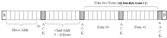
I2C Master 62

SPI Master 64

External Digital Trigger 67

Trigger Out 68

Event Out 69

Handshake 70

Sample Clock In/Out 71

3.10 Pattern Match.... 72

3.11 COS (Change of State) Event 74

3.12 Termination 75

# AppendixA ADLINK DIN-68H 77

# Important Safety Instructions.... 81

# Getting Service 83

# List of Figures

Figure 1-1: Acquisition Timing Diagram....7

Figure 1-2: Generation Timing Diagram....8

Figure 1-3: PCIe-7360 Schematic Diagram 12

Figure 1-4: PCIe-7360 Connectors 13

Figure 3-1: PCIe-7360 Block Diagram 22

Figure 3-2: DI Raw Data Mapping for 8-Bit Data Width ..... 25

Figure 3-3: DI raw data Mapping for 16-Bit Data Width ..... 26

Figure 3-4: DI raw data Mapping for 24-Bit Data Width ..... 27

Figure 3-5: DI raw data Mapping for 32-Bit Data Width ..... 27

Figure 3-6: Phase Shift of Sample Clock 28

Figure 3-7: Maximum Data Throughput 29

Figure 3-8: Scatter-Gather DMA for Data Transfer 31

Figure 3-9: DI/DO Sample Clock Architecture 34

Figure 3-10: DI Continuous Mode Architecture.... 37

Figure 3-11: DI Timing Diagram....38

Figure 3-12: DO Continuous Mode Architecture 40

Figure 3-13: DO Timing Diagram....41

Figure 3-14: DI Handshake Mode Architecture....43

Figure 3-15: DI Handshake Timing Diagram....44

Figure 3-16: DO Handshake Mode Architecture 46

Figure 3-17: DO Handshake Timing Diagram....47

Figure 3-18: DI Burst Handshake Mode Architecture ....49

Figure 3-19: DI Burst Handshake Timing Diagram .... 50

Figure 3-20: DO Burst Handshake Mode Architecture....52

Figure 3-21: DO Burst Handshake Timing Diagram ....53

Figure 3-22: DO Burst Handshake 2 Timing Diagram .... 53

Figure 3-23: DI Post Trigger....54

Figure 3-24: DO Post Trigger....55

Figure 3-25: DI Post Trigger with Re-trigger 55

Figure 3-26: DO Post Trigger with Re-Trigger 56

Figure 3-27: DI Gated Trigger 56

Figure 3-28: DO Gated Trigger 57

Figure 3-29: I2C Master of PCIe-7360 62

Figure 3-30: Data Transfer on the I2C Bus 63

Figure 3-31: I2C Data Format 64

Figure 3-32: SPI Master of PCIe-7360....65

Figure 3-33: Data Transfer on SPI Bus....66

Figure 3-34: Clock Mode of SCK 66

Figure 3-35: External Digital Trigger Input Configuration....67

Figure 3-36: Configured AFI as Internal Software Trigger Output ..... 68

Figure 3-37: Pattern Match and COS Event Configuration ....69

Figure 3-38: Configured AFI as Handshake Interface....70

Figure 3-39: Configured AFI7 as DI Sampled Clock In/Out ..... 71

Figure 3-40: Configured AFI6 as DO Sampled Clock In/Out .....72

Figure 3-41: Example of Pattern Matching....74

Figure 3-42: Example of Pattern Match ....75

Figure A-1: DIN-68H Layout 77

Figure A-2: Resistor Termination Schematic....78

Figure A-3: DIN-68H Layout (Back Side) 79

# List of Tables

Table 1-1: PCIe-7360 SCSI-VHDCI 68-pin Assignment.... 15
Table 1-2: Signal Descriptions for SCSI-VHDCI and SMB Connectors....16
Table 1-3: SMB Jack Connector Signal Description.... 17
Table 1-4: LED indicator 17
Table 3-1: Logic Levels....23
Table 3-2: DI/DO Sample Clock Configuration 35
Table A-1: DIN-68H Pin Assignment 77
Table A-2: Pad Position of User-Defined Resistor Termination ..... 79

This page intentionally left blank.

# 1 Introduction

ADLINK's PCIe-7360 is a high-speed digital I/O board with 32-channel bi-directional parallel I/O lines. Data rate up to 400 MB/s is available through the x4 PCI Express® interfaces, with clock rate up to 100 MHz internal clock or 200 MHz external clock, ideally suited for high-speed and large scale digital data acquisition or exchange applications, such as digital image capture, video playback, and IC testing.

# 1.1 Features

▶ x4 lane PCI Express® interface
▶ 8/16/24/32-CH @ up to 100MHz for DI or DO and 8/16-CH @ up to 200MHz for DI in external clock mode
▶ 400 MB/s maximum throughput
▶ Software selectable 1.8 V, 2.5 V, or 3.3 V (5 V compatible) voltage levels
▶ 80-step phase shift in external clock mode
▶ Per group (8-bit) input/output direction selectable
▶ Supports I2C and SPI programmable serial interfaces for external device communication
▶ Scatter-gather DMA support
▶ Flexible handshake and external digital trigger modes
▶ 8-channel auxiliary programmable I/O support

# 1.2 Applications

▶ High-speed digital data exchange
▶ Digital pattern generation and acquisition
▶ IC testing
▶ Interface to external high-speed A/D and D/A converter
▶ ATE

# 1.3 Specifications

# 1.3.1 General

<table><tr><td>Interface</td><td colspan="3">x4 PCI Express interface</td></tr><tr><td>Connectors</td><td colspan="3">SMB Jack Connector x2 (CLK IN &amp; OUT)68-pin SCSI-VHDCI x1 (32-bit Data Lines &amp; 8-CH AFI)</td></tr><tr><td>Operating Temperature</td><td colspan="3">0°C - 55°C</td></tr><tr><td>Storage Temperature</td><td colspan="3">-20°C - 70°C</td></tr><tr><td>Humidity</td><td colspan="3">5 - 95%, non-condensing</td></tr><tr><td>Dimensions</td><td colspan="3">168 mm (L) x 112 mm (H), not including connectors</td></tr><tr><td rowspan="4">Power Consumption</td><td></td><td>Typical</td><td>Maximum</td></tr><tr><td>+3.3 VDC</td><td>860 mA</td><td>950 mA</td></tr><tr><td>+12V VDC</td><td>270 mA</td><td>550 mA</td></tr><tr><td>Total Power</td><td>6.1 W</td><td>9.8 W</td></tr></table>

# 1.3.2 Digital I/O

<table><tr><td colspan="2">Channels</td><td colspan="3">32</td></tr><tr><td colspan="2">Direction(programmable)</td><td colspan="3">Input or output, per group (8 channel) basis</td></tr><tr><td colspan="2">Logic level(programmable)</td><td>1.8 V</td><td>2.5 V</td><td>3.3 V(5 V compatible)</td></tr><tr><td rowspan="2">Input voltage</td><td>Min. $V_{IH}$ </td><td>1.2 V</td><td>1.6 V</td><td>2 V</td></tr><tr><td>Max. $V_{IL}$ </td><td>0.63 V</td><td>0.7 V</td><td>0.8 V</td></tr><tr><td rowspan="2">Output voltage</td><td>Min. $V_{OH}$ </td><td>1.6 V</td><td>2.3 V</td><td>3.1 V</td></tr><tr><td>Max. $V_{OL}$ </td><td>0.2 V</td><td>0.2 V</td><td>0.2 V</td></tr><tr><td colspan="2">Driving capacity(min.)</td><td>±8 mA</td><td>±16 mA</td><td>±32 mA</td></tr><tr><td colspan="2">Max. throughput</td><td colspan="3">Digital input: 400M Byte/sDigital output: 400M Byte/s</td></tr><tr><td colspan="2">Buffer size</td><td colspan="3">Digital input: 8k samplesDigital output: 20k samples</td></tr><tr><td colspan="2">Data transfer</td><td colspan="3">Software pollingBus-mastering DMA with scatter-gather</td></tr><tr><td colspan="2">Clock modes</td><td colspan="3">Internal clock: up to 100 MHzExternal clock: 200 MHz for DI, 100MHz for DO (see Note)HandshakeBurst handshake</td></tr><tr><td colspan="2">Trigger source</td><td colspan="3">SoftwareExternal digital signalPattern match</td></tr><tr><td colspan="2">Trigger modes</td><td colspan="3">Post trigger with re-triggerGate trigger</td></tr><tr><td colspan="2">Input impedance</td><td colspan="3">10 kΩ</td></tr><tr><td colspan="2">Input protection range</td><td colspan="3">-1 to 6 V</td></tr><tr><td colspan="2">Input protection range</td><td colspan="3">-1 to 6 V</td></tr><tr><td colspan="2">Output impedance</td><td colspan="3">50 Ω</td></tr><tr><td colspan="2">Power-up initial state</td><td colspan="3">Tri-state/All digital inputs</td></tr><tr><td colspan="2">Output protection range</td><td colspan="3">-0.5 V to 3.8 V</td></tr></table>

![](.pcie-7360-50-11042-1000-200-en/9167b6f2edbeef71e5545198089f855102c5776d382b7b2809f140378e65e710.jpg)
NOTE:

External clock rate, which can be up to 200 MHz, only supports 8 or 16-bit data width

# 1.3.3 Application Function I/O (AFI)

<table><tr><td colspan="2">Channels</td><td colspan="3">8</td></tr><tr><td colspan="2">Direction (programmable)</td><td colspan="3">Input or output, per channel basis</td></tr><tr><td colspan="2">Logic levels (programmable)</td><td>1.8 V</td><td>2.5 V</td><td>3.3 V (5 V compatible)</td></tr><tr><td rowspan="2">Input voltage</td><td>Min.  $V_{IH}$ </td><td>1.2 V</td><td>1.6 V</td><td>2 V</td></tr><tr><td>Max.  $V_{IL}$ </td><td>0.63 V</td><td>0.7 V</td><td>0.8 V</td></tr><tr><td rowspan="2">Output voltage</td><td>Min.  $V_{OH}$ </td><td>1.6 V</td><td>2.3 V</td><td>3.1 V</td></tr><tr><td>Max.  $V_{OL}$ </td><td>0.2 V</td><td>0.2 V</td><td>0.2 V</td></tr><tr><td colspan="2">Driving capacity (max.)</td><td>±8 mA</td><td>±16 mA</td><td>±32 mA</td></tr><tr><td colspan="2">Input impedance</td><td colspan="3">10 kΩ</td></tr><tr><td colspan="2">Input protection range</td><td colspan="3">-1 to 6 V</td></tr><tr><td colspan="2">Output impedance</td><td colspan="3">50 Ω</td></tr><tr><td colspan="2">Power-up initial state</td><td colspan="3">Tri-state/All digital inputs</td></tr><tr><td colspan="2">Output protection range</td><td colspan="3">-0.5V to 3.8V</td></tr><tr><td colspan="2">Supported Modes (programmable)</td><td colspan="3"> $I^{2}C$  masterSPI masterHandshakeExternal trigger in/outDI/DO sample clock in/out</td></tr></table>

# 1.3.4 Timing Specifications

<table><tr><td colspan="2">Sample Clock</td></tr><tr><td>Clock sources</td><td>Internal clock: onboard 100MHz with 16-bit dividerExternal clock: AFI6 (for DO)AFI7 (for DI)SMB CLK in</td></tr><tr><td>Internal clock rate(programmable)</td><td>1526 Hz – 100 MHz (100 MHz/ N;1≤N≤65,535)</td></tr><tr><td>Ext. frequency range</td><td>Phase shift disabled: 0-200 MHzPhase shift enabled: 20MHz - 100MHz (see Note)</td></tr><tr><td>Phase shift</td><td>Internal clock: N/AExternal clock: 80 steps; 1 step = 4.5°</td></tr><tr><td colspan="2">Sample Clock Exporting</td></tr><tr><td>Destination</td><td>AFI6 (for DO)AFI7 (for DI)SMB CLK out</td></tr><tr><td>Frequency range</td><td>Phase shift disabled: 0-100 MHzPhase shift enabled: 20MHz - 100MHz (see Note)</td></tr><tr><td>Clock jitter</td><td>Period jitter: 300 ps</td></tr><tr><td>Clock duty cycle</td><td>50%</td></tr><tr><td>Phase shift resolution</td><td>1/80 of external sampled clock period (80 steps; 1 step = 4.5°)</td></tr></table>

![](.pcie-7360-50-11042-1000-200-en/31c0782756edf5dcd91b95aa1cdb5378fabd89fced7dc1c435193e3d6646423f.jpg)
NOTE:

When phase shift is enabled, the clock must be continuous and free-running

# 1.3.5 Timing Accuracy

<table><tr><td colspan="2">Acquisition Timing</td></tr><tr><td>Channel-to-Cannel skew</td><td>±1.08 ns</td></tr><tr><td>Setup time to sampled clock ( $t_{SU}$ )</td><td>2 ns</td></tr><tr><td>Hold time to sampled clock ( $t_{H}$ )</td><td>2 ns</td></tr><tr><td>Time delay of external sampled clock from AFI7 to internal ( $t_{AF7D}$ )</td><td>6.3 ns</td></tr><tr><td>Time delay of external sampled clock from SMB CLK in to internal ( $t_{SMBID}$ )</td><td>9.1 ns</td></tr><tr><td>Time delay of DI data from VHDCI connector to internal ( $t_{DID}$ )</td><td>3.26 ns - 4.34 ns</td></tr><tr><td colspan="2">Generation Timing</td></tr><tr><td>Exported clock skew AFI6 -to- SMB CLK out ( $t_{ECskew}$ )</td><td>2 ns</td></tr><tr><td>Exported clock (AFI6) -to- DO data delay ( $t_{AF62D}$ )</td><td>600 ps - 5 ns</td></tr></table>

![The diagram illustrates the timing of clock and data signals as they pass through a delay.\n\n**Labeled Blocks and Signals:**\n*   **Top Section:**\n    *   'DI Sampled Clock (AFI7)': A square wave signal.\n    *   'DI Data (connector)': A sequence of hexagonal blocks labeled 'D0', 'D1', 'D2', and 'D3'.\n    *   Timing labels: 't_SU' and 't_H' appear between the rising edge of the clock and the 'D0' block.\n*   **Middle Transition:**\n    *   A large grey arrow pointing downward labeled 'Trace & component delay'.\n    *   A timing label 't_AF7D' indicating a shift in the clock signal.\n*   **Bottom Section:**\n    *   'DI Sampled Clock (into FPGA)': A square wave signal shifted to the right relative to the top clock.\n    *   'DI Data (into FPGA)': A sequence of hexagonal blocks labeled 'D0', 'D1', 'D2', and 'D3'.\n    *   Timing label: 't_DID' appears near the alignment of the clock and 'D0' block.\n\n**Connections and Relationships:**\n*   Vertical dotted lines connect the rising edges of the clocks in the top and bottom sections to specific points on the data blocks ('D0').\n*   The 'Trace & component delay' arrow indicates the transformation from the top signals ('connector') to the bottom signals ('into FPGA').\n*   Hatched grey regions precede the 'D0' block in both the 'DI Data (connector)' and 'DI Data (into FPGA)' rows.](.pcie-7360-50-11042-1000-200-en/264844676c198160da9f8366b3c4a141bd9024f7f97dec8faa222769d0f463aa.jpg)

$t_{AF7D}$ = Time delay of external sampled clock from AFI7 to internal
$t_{DID}$ = Time delay of DI data from VHDCI connector to internal

Figure 1-1: Acquisition Timing Diagram

![Based on the provided timing diagram, here is the accurate description of the labeled elements and their connections:\n\n**Labeled Waveforms (from top to bottom):**\n1.  **DO Sampled Clock (internal)**\n2.  **Exported DO Sampled Clock (SMB CLK out/ non-inverted)**\n3.  **Exported DO Sampled Clock (AFI6/ non-inverted)**\n4.  **Exported DO Sampled Clock (AFI6/ inverted)**\n5.  **Exported DO Sampled Clock (AFI6/ phase delay)**\n6.  **DO Data** (showing data blocks labeled **D0**, **D1**, and **D2**)\n\n**Connections and Timing Annotations:**\n*   **Generation Start**: A vertical dotted line marks the start point at the top.\n*   **Trace & component delay**: A large grey arrow points downward from the internal clock to the exported SMB clock.\n*   **t_SC2AF6** and **t_ECskey**: Horizontal arrows indicate timing differences between the 'SMB CLK out' and 'AFI6/ non-inverted' clocks.\n*   **Phase delay (0° ~ 360°)**: A horizontal arrow indicates the phase shift between the 'AFI6/ inverted' and 'AFI6/ phase delay' clocks.\n*   **t_AF62D**: A horizontal arrow indicates the timing difference between the phase-delayed clock and the data start.\n*   **Write data to external device**: A long horizontal arrow at the bottom spans from the 'Generation Start' line to the end of the data sequence.](.pcie-7360-50-11042-1000-200-en/bf46d230fe763bd0aef8717603b19f8f2de2d275ce6ef295c18b8f684267afe1.jpg)

$t_{SC2AF6}$ = Time delay from sampled clock (internal) to exported sampled clock (AFI6)
$t_{ECskew}$ = Time delay from exported clock (AFI6) to exported clock (SMB CLK out)
$t_{AF62D}$ = Time delay from exported sampled clock (AFI6) to do data

Figure 1-2: Generation Timing Diagram

# 1.3.6 External Clock I/O Specification

<table><tr><td colspan="3">CLK IN (SMB Jack Connector)</td></tr><tr><td>Destination</td><td colspan="2">DI or DO sample clock</td></tr><tr><td>Input coupling</td><td colspan="2">AC</td></tr><tr><td>Input Impedance</td><td colspan="2">50 Ω</td></tr><tr><td>Minimum detectable pulse width</td><td colspan="2">8 ns</td></tr><tr><td rowspan="7">External sampled clock range</td><td colspan="2">Square Wave</td></tr><tr><td>Voltage</td><td>0.2 Vpp to 5 Vpp</td></tr><tr><td>Frequency</td><td>Phase shift disabled: 0-200 MHzPhase shift enabled: 20MHz - 100MHz</td></tr><tr><td>Duty cycle</td><td>40% - 60%</td></tr><tr><td colspan="2">Sine Wave</td></tr><tr><td>Voltage</td><td>0.2 Vpp to 5 Vpp</td></tr><tr><td>Frequency</td><td>Phase shift disabled: 0-200 MHzPhase shift enabled: 20MHz - 100MHz</td></tr><tr><td colspan="3">CLK OUT (SMB Jack Connector)</td></tr><tr><td>Sources</td><td colspan="2">DI or DO internal sample clock</td></tr><tr><td>Source impedance</td><td colspan="2">50 Ω</td></tr><tr><td>Logic Levels (programmable)</td><td colspan="2">The same logic level of AFI I/O (1.8 V, 2.5 V, or 3.3 V)</td></tr><tr><td>Driving Capacity (Max.)</td><td colspan="2">±8 mA at 1.8 V±16 mA at 2.5 V±32 mA at 3.3 V</td></tr></table>

# 1.3.7 I²C Master Specification

<table><tr><td rowspan="3">Signal</td><td></td><td>Direction</td><td colspan="2">Pin</td></tr><tr><td>SCL</td><td>O</td><td colspan="2">AFI0</td></tr><tr><td>SDA</td><td>I/O</td><td colspan="2">AFI1</td></tr><tr><td colspan="2">Supported clock rate(programmable)</td><td colspan="3">1.9 kHz -244.14 kHz;488.28125 kHz / (n + 1); 1 ≤ n ≤ 255</td></tr><tr><td colspan="2">Transfer size of Data</td><td colspan="3">0 - 4 Bytes</td></tr><tr><td colspan="2">Transfer size of Cmd/ Addr</td><td colspan="3">0 - 4 Bytes</td></tr><tr><td colspan="2">Logic families (programmable)</td><td>1.8 V</td><td>2.5 V</td><td>3.3 V</td></tr><tr><td rowspan="2">Input Voltage</td><td>Min.  $V_{IH}$ </td><td>1.2 V</td><td>1.6 V</td><td>2.0 V</td></tr><tr><td>Max.  $V_{IL}$ </td><td>0.63 V</td><td>0.7 V</td><td>0.8 V</td></tr><tr><td rowspan="2">Output Voltage</td><td>Min.  $V_{OH}$ </td><td>1.6 V</td><td>2.3 V</td><td>3.1 V</td></tr><tr><td>Max.  $V_{OL}$ </td><td>0.2 V</td><td>0.2 V</td><td>0.2 V</td></tr></table>

# 1.3.8 SPI Master Specification

<table><tr><td rowspan="5">Signal</td><td></td><td></td><td>Direction</td><td>Pin</td></tr><tr><td></td><td>SCK</td><td>O</td><td>AFI0</td></tr><tr><td></td><td>SDO</td><td>O</td><td>AFI1</td></tr><tr><td></td><td>SDI</td><td>I</td><td>AFI2</td></tr><tr><td></td><td>CS_0</td><td>O</td><td>AFI3</td></tr><tr><td colspan="2">Supported clock rate(programmable)</td><td colspan="3">244.14 kHz -62.5 MHz,62.5 MHz / (n + 1); 0 ≤ n ≤ 255</td></tr><tr><td colspan="2">Clock mode</td><td colspan="3">&lt;img src="images/686b6bb691c10aee2957f21c46f1125e60a52ea044daa032f143b630c05a13dd.jpg"/&gt;</td></tr><tr><td colspan="2">The first bit be transferred</td><td colspan="3">MSB/ LSB(Default: MSB)</td></tr><tr><td colspan="2">Transfer size of Data</td><td colspan="3">0 - 32 bits</td></tr><tr><td colspan="2">Transfer size of Cmd/ Addr</td><td colspan="3">0 - 32 bits</td></tr><tr><td colspan="2">Dummy size</td><td colspan="3">0 - 15 bits</td></tr><tr><td colspan="2">SPI Slave selection</td><td colspan="3">CS_0</td></tr><tr><td colspan="2">Logic families(programmable)</td><td>1.8 V</td><td>2.5 V</td><td>3.3 V</td></tr><tr><td rowspan="2">Input Voltage</td><td>Min. VIH</td><td>1.2 V</td><td>1.6 V</td><td>2 V</td></tr><tr><td>Max. VIL</td><td>0.63 V</td><td>0.7 V</td><td>0.8 V</td></tr><tr><td rowspan="2">Output Voltage</td><td>Min. VOH</td><td>1.6 V</td><td>2.3 V</td><td>3.1 V</td></tr><tr><td>Max. VOL</td><td>0.2 V</td><td>0.2 V</td><td>0.2 V</td></tr></table>

# 1.4 Software Support

ADLINK provides versatile software drivers and packages for users' different approach to building up a system. ADLINK not only provides programming libraries such as DLL for most Windows based systems, but also provide drivers for other software packages such as LabVIEW®.

All software options are included in the ADLINK CD. Non-free software drivers are protected with licensing codes. Without the software code, you can install and run the demo version for two hours for trial/demonstration purposes. Please contact ADLINK dealers to purchase the formal license.

# DAQPilot

DAQPilot is ADLINK's proprietary task-oriented software development kit (SDK), supporting ActiveX Controls/.NET Assembly, Express VI and Polymorphic VI for LabVIEW and DAQ Toolbox for MATLAB.

You can download and install DAQPilot at:

http://www.adlinktech.com/TM/DAQPilot.html

Please note that only DAQPilot versions 2.6.1.0705 and later support the PCIe-7360.

# PCIS-DASK

PCIS-DASK comprises advanced 32/64-bit kernel drivers for customized DAQ application development, enabling detailed operations and superior performance and reliability from the data acquisition system. DASK kernel drivers now support Windows 8/7/XP OS.

Please note that only PCIS-DASK versions 5.10 and later support the PCIe-7360 module.

# 1.5 Schematics, I/O and Indicators

![The image displays a simple graphic of a white piece of paper with a folded top-right corner. Faint grey horizontal lines run across the paper, resembling a document or list. A large, bold red checkmark is superimposed diagonally over the center of the paper.](.pcie-7360-50-11042-1000-200-en/1a928bcce83d7e600f8fea7446f3e1798b8275bc4bf1d8c9f9173d0986f8e2a2.jpg)
NOTE:

All dimensions shown are in mm

![100.36\n176.42\n111.15](.pcie-7360-50-11042-1000-200-en/febeecc3e09b5d2b58b869315f227e4ca59b7435017c9396ac34182700a7385e.jpg)

Figure 1-3: PCIe-7360 Schematic Diagram

# 1.6 Connectors

The PCIe-7360 card is equipped with one 68-pin SCSI-VHDCI connector for high-speed digital I/O and programmable function

I/O, and two SMB connectors for sample clock input and output, as labeled on the faceplate.

![ACC\nCLK IN\nCLK OUT\nDIO](.pcie-7360-50-11042-1000-200-en/c9251f66f9ef6262f885d66b841c517826c37803621bf330a2fb8c77c602a243.jpg)

Figure 1-4: PCIe-7360 Connectors

<table><tr><td>ID</td><td>Pin</td><td>Pin</td><td>ID</td></tr><tr><td>GND</td><td>68</td><td>34</td><td>GND</td></tr><tr><td>(DI CLK) AFI7</td><td>67</td><td>33</td><td>AFI6 (DO CLK)</td></tr><tr><td>GND</td><td>66</td><td>32</td><td>GND</td></tr><tr><td>D0</td><td>65</td><td>31</td><td>D1</td></tr><tr><td>AFI5</td><td>64</td><td>30</td><td>AFI4</td></tr><tr><td>D2</td><td>63</td><td>29</td><td>D3</td></tr><tr><td>GND</td><td>62</td><td>28</td><td>GND</td></tr><tr><td>D4</td><td>61</td><td>27</td><td>D5</td></tr><tr><td>AFI3</td><td>60</td><td>26</td><td>AFI2</td></tr><tr><td>D6</td><td>59</td><td>25</td><td>D7</td></tr><tr><td>GND</td><td>58</td><td>24</td><td>GND</td></tr><tr><td>D8</td><td>57</td><td>23</td><td>D9</td></tr><tr><td>GND</td><td>56</td><td>22</td><td>GND</td></tr><tr><td>D10</td><td>55</td><td>21</td><td>D11</td></tr><tr><td>GND</td><td>54</td><td>20</td><td>GND</td></tr><tr><td>D12</td><td>53</td><td>19</td><td>D13</td></tr><tr><td>AFI1</td><td>52</td><td>18</td><td>GND</td></tr><tr><td>D14</td><td>51</td><td>17</td><td>D15</td></tr><tr><td>GND</td><td>50</td><td>16</td><td>GND</td></tr><tr><td>D16</td><td>49</td><td>15</td><td>D17</td></tr><tr><td>GND</td><td>48</td><td>14</td><td>GND</td></tr><tr><td>D18</td><td>47</td><td>13</td><td>D19</td></tr><tr><td>GND</td><td>46</td><td>12</td><td>GND</td></tr><tr><td>D20</td><td>45</td><td>11</td><td>D21</td></tr><tr><td>GND</td><td>44</td><td>10</td><td>GND</td></tr><tr><td>D22</td><td>43</td><td>9</td><td>D23</td></tr><tr><td>GND</td><td>42</td><td>8</td><td>AFI0</td></tr><tr><td>D24</td><td>41</td><td>7</td><td>D25</td></tr><tr><td>GND</td><td>40</td><td>6</td><td>GND</td></tr><tr><td>D26</td><td>39</td><td>5</td><td>D27</td></tr><tr><td>GND</td><td>38</td><td>4</td><td>GND</td></tr></table>

<table><tr><td>ID</td><td>Pin</td><td>Pin</td><td>ID</td></tr><tr><td>D28</td><td>37</td><td>3</td><td>D29</td></tr><tr><td>GND</td><td>36</td><td>2</td><td>GND</td></tr><tr><td>D30</td><td>35</td><td>1</td><td>D31</td></tr></table>

Table 1-1: PCIe-7360 SCSI-VHDCI 68-pin Assignment

<table><tr><td>Pin</td><td>Signal</td><td>Signal Type</td><td>Direction</td><td>Description</td></tr><tr><td>25, 27, 29, 31, 59, 61, 63, 65</td><td>D0 – D7</td><td>Data</td><td>I/O</td><td>Port_A bi-directional digital data lines</td></tr><tr><td>17, 19, 21, 23, 51, 53, 55, 57</td><td>D8 – D15</td><td>Data</td><td>I/O</td><td>Port_B bi-directional digital data lines</td></tr><tr><td>9, 11, 13, 15, 43, 45, 47, 49</td><td>D16 – D23</td><td>Data</td><td>I/O</td><td>Port_C bi-directional digital data lines</td></tr><tr><td>1, 3, 5, 7, 35, 37, 39, 41</td><td>D24 – D31</td><td>Data</td><td>I/O</td><td>Port_D bi-directional digital data lines</td></tr><tr><td>8, 26, 30, 52, 60, 64</td><td>AFI0 – AFI5</td><td>Control /Data</td><td>I/O</td><td>Application Function I/O, can be configured as:►  $I^{2}C$ / SPI► Handshake signal► External trigger in/out► Event out</td></tr></table>

<table><tr><td>Pin</td><td>Signal</td><td>Signal Type</td><td>Direction</td><td>Description</td></tr><tr><td>33</td><td>AFI6</td><td>Control /Data</td><td>I/O</td><td>Application Function I/O, can be configured as: ►Handshake signal ►External trigger in/out ►Event out ►DO sampled clock in/out</td></tr><tr><td>67</td><td>AFI7</td><td>Control /Data</td><td>I/O</td><td>Application Function I/O, can be configured as: ►Handshake signal ►External trigger in/out ►Event out ►DI sampled clock in/out</td></tr><tr><td>2, 4,6, 10, 12, 14, 16, 18,20, 22, 24, 28, 32, 34, 36, 38, 40, 42, 44, 46, 48, 50, 54, 56, 58, 62, 66, 68</td><td>GND</td><td>Ground</td><td>N/A</td><td>Ground reference for Data I/O and AFI I/O</td></tr></table>

Table 1-2: Signal Descriptions for SCSI-VHDCI and SMB Connectors

<table><tr><td>Signal</td><td>Signal Type</td><td>Direction</td><td>Description</td></tr><tr><td>CLK IN</td><td>Clock</td><td>I</td><td>External clock input for DI/DO sampled clock from external device to the PCIe-7360</td></tr><tr><td>CLK OUT</td><td>Clock</td><td>O</td><td>DI/DO sampled clock exporting from the PCIe-7360 to an external device</td></tr></table>

Table 1-3: SMB Jack Connector Signal Description

# 1.7 LED indicator

The LED on the faceplate indicates I2C & SPI communication and digital I/O status of the PCIe-7360.

<table><tr><td>LED</td><td>Color</td><td>Mode</td></tr><tr><td rowspan="3">ACC (Access)</td><td>Red</td><td>DI DMA operation</td></tr><tr><td>Green</td><td>DO DMA operation</td></tr><tr><td>Amber</td><td>DI &amp; DO DMA operation</td></tr></table>

Table 1-4: LED indicator

This page intentionally left blank.

# 2 Getting Started

# 2.1 Unpacking Checklist

Before unpacking, check the shipping carton for any damage. If the shipping carton and/or contents are damaged, inform your dealer immediately. Retain the shipping carton and packing materials for inspection. Obtain authorization from your dealer before returning any product to ADLINK. Check if the following items are included in the package.

▶ PCIe-7360 high-speed DIO card
▶ ADLINK All-in-One CD
▶ Quick Start Guide

If any of the items is damaged or missing, contact your dealer immediately.

![The image displays a yellow triangular warning sign with a black border and a large black exclamation point in the center. Below the triangle, the text 'CAUTION:' is printed in black capital letters.](.pcie-7360-50-11042-1000-200-en/9d3632664987674e3a9854807b99ff9e50553f5c0ba0b821099e742188a45b22.jpg)

The card must be protected from static discharge and physical shock. Never remove any of the socketed parts except at a static-free workstation. Use the anti-static bag shipped with the product to handle the card. Wear a grounded wrist strap when servicing.

# 2.2 Installing the Card

Install the card driver before you install the card into your computer system. See “Software Support” on page 11. for driver support information.

To install the card:

1. Turn off the system/chassis and disconnect the power plug from the power source.
2. Remove the system/chassis cover.
3. Select the PCI Express slot that you intend to use, then remove the bracket opposite the slot, if any.
4. Align the card connectors (golden fingers) with the slot, then press the card firmly until the card is completely seated on the slot.

5. Secure the card to the chassis with a screw.
6. Replace the system/chassis cover.

7. Connect the power plug to a power source, then turn on the system.

# Configuration

All PCI/PCI Express cards on your system are configured individually. Because configuration is controlled by the system and the software, no jumper setting is required for base address, DMA, and interrupt IRQ. Configuration is subject to change with every boot of the system as new PCI/PCI Express $^{®}$ cards are added or removed.

# Troubleshooting

If your system fails to boot or if you experience erratic operation with your PCI/PCI Express card in place, an interrupt conflict may have been generated (such as when the BIOS Setup is incorrectly configured). Refer to the system's BIOS documentation for details.

# 2.3 Selecting Cables and Termination Board

Since the PCIe-7360 is a high-speed digital I/O card, impedance matching is important in eliminating signal reflection generated by cabling or PCB trace. The following recommended cables and termination board can improve signal quality during high-speed signal transfer.

DIN-68H – Termination board with one 68-pin SCSI-VHDCI connector and user selectable impedance. See “ADLINK DIN-68H” on page 77. for more information.

ACL-10279 - 68-pin SCSI-VHDCI cable with $50\Omega$ impedance

SMB-SMB-1M – SMB to SMB cable, 1 M, for sample clock in/out

SMB-BNC-1M – SMB to BNC cable, 1 M, for sample clock in/out

# 3 Operations

The PCIe-7360 provides functions including high-speed digital pattern acquisition, digital pattern generation, application function I/O, and others.

# 3.1 Block Diagram

The PCIe-7360 provides 32-channel bi-directional high-speed digital I/O lines, 8-channel AFI (Application Function I/O) lines, and two sample clock input/output channels. All 32-channel high-speed digital I/O lines are connected to the level shifter and can be programmed as 1.8 V, 2.5 V, or 3.3 V (5 V compatible) logic levels. These channels can also be programmed as input channels for digital pattern acquisition or output channels for digital pattern generation.

8-channel application function I/O lines are also connected to the level shifter. These application function I/Os can be programmed as I2C or SPI serial interface, handshake interface, external digital trigger input, event output and external clock input/output with 1.8 V or 2.5 V or 3.3 V (5 compatible) logic levels by direction and logic level control of level shifter and by AFI controller implemented in FPGA.

The digital pattern acquisition/generation and corresponding flexible sample timing are controlled by ADLINK's Smart Control Engine implemented by FPGA, as shown

![Based on the provided image, here is the accurate and concise description of the flowchart, including all labeled blocks and connections with verbatim text:\n\n**Labeled Blocks:**\n\n*   **100MHz OSC** (Pink circle)\n*   **SMB IN** (Pink connector icon)\n*   **SMB OUT** (Pink connector icon)\n*   **80-Step Phase Shift Control** (Red rectangle)\n*   **Pattern Acquisition/ Generation Timing Control** (Large light blue rectangle)\n    *   Contains: **DI Latch**, **8K FIFO**, **DI DMA**, **Logic Level Control**, **ADLINK Smart Control Engine**, **PCIe INTERFACE**, **DO Buffer**, **20K FIFO**, **DO DMA**, **I2C/SPI**, **AFI Interface**\n*   **1.8/2.5/3.3V Logic Level Selectable** (Top orange rectangle)\n    *   Contains four **Level Shifter** blocks\n*   **1.8/2.5/3.3V Logic Level Selectable** (Bottom orange rectangle)\n    *   Contains two **Level Shifter** blocks\n*   **VHDC1-68P CONNECTOR INTERFACE** (Large vertical blue arrow on the far left)\n*   **PCI Express x4 INTERFACE** (Large vertical blue arrow on the far right)\n\n**Connections:**\n\n*   **100MHz OSC** connects via a purple line labeled 'Int. Timebase' to **80-Step Phase Shift Control** and **Pattern Acquisition/ Generation Timing Control**.\n*   **SMB IN** connects via a purple line labeled 'Ext. CLK in' to **80-Step Phase Shift Control**.\n*   **SMB OUT** connects via a purple line labeled 'Ext. CLK out' from **80-Step Phase Shift Control**.\n*   **80-Step Phase Shift Control** connects to **Pattern Acquisition/ Generation Timing Control** via a purple line labeled 'Ext. CLK in/out'.\n*   **80-Step Phase Shift Control** connects to the top **1.8/2.5/3.3V Logic Level Selectable** block via a purple line.\n*   The top **1.8/2.5/3.3V Logic Level Selectable** block connects to **DI Latch** via a thick blue line labeled 'DI DATA'.\n*   **DO Buffer** connects to the top **1.8/2.5/3.3V Logic Level Selectable** block via a thick blue line labeled 'DO DATA'.\n*   **DI Latch** connects to **8K FIFO** via a rightward arrow.\n*   **8K FIFO** connects to **DI DMA** via a rightward arrow.\n*   **20K FIFO** connects to **DO Buffer** via a leftward arrow.\n*   **I2C/SPI** connects to the green line labeled 'AFI BUS' via a thick pink downward arrow.\n*   **AFI Interface** connects to the green line labeled 'AFI BUS' via a thick green upward-right arrow.\n*   The green line labeled 'AFI BUS' connects to the bottom **1.8/2.5/3.3V Logic Level Selectable** block.\n*   The bottom **1.8/2.5/3.3V Logic Level Selectable** block connects to external lines labeled 'AFI(5:0)' and 'AFI(7:6)'.\n*   The top **1.8/2.5/3.3V Logic Level Selectable** block connects to external lines labeled 'DIO(7:0)', 'DIO(15:8)', 'DIO(23:16)', and 'DIO(31:24)'.\n*   **PCIe INTERFACE** connects to **PCI Express x4 INTERFACE** via a double-headed blue arrow.\n*   The DIO connections ('DIO(7:0)', etc.) are encompassed by the vertical arrow labeled **VHDC1-68P CONNECTOR INTERFACE**.](.pcie-7360-50-11042-1000-200-en/866dba4c5f147590799b82b7696c1cbee4239379ed46971a89f24de84d25f124.jpg)

Figure 3-1: PCIe-7360 Block Diagram

# 3.2 Programmable Logic Level

To interface different logic level applications, the PCIe-7360 supports three software selectable logic levels of 1.8 V, 2.5 V, or 3.3 V (5 V compatible) for all digital I/O lines, sample clocks, $I^{2}C$ , SPI, triggers, and events. All I/O lines conform to the selected logic level. When connecting PCIe-7360 to a device under test (DUT), interface voltage levels must be compatible, as follows.

▶ $V_{IH}$ : The digital input voltage at logic high; senses a binary one (1)
▶ $V_{IL}$ : The digital input voltage at logic low; senses a binary zero (0)
▶ $V_{OH}$ : The digital output voltage at logic high; generates a binary one (1)
▶ $V_{OL}$ : The digital output voltage at logic low; generates a binary zero (0)

<table><tr><td colspan="2">Logic Levels</td><td>1.8 V</td><td>2.5 V</td><td>3.3 V(5 V compatible)</td></tr><tr><td rowspan="2">Digital Input</td><td>Min. VIH</td><td>1.2 V</td><td>1.6 V</td><td>2 V</td></tr><tr><td>Max. VIL</td><td>0.63 V</td><td>0.7 V</td><td>0.8 V</td></tr><tr><td rowspan="2">Digital Output</td><td>Min. VOH</td><td>1.6 V</td><td>2.3 V</td><td>3.1 V</td></tr><tr><td>Max. VOL</td><td>0.2 V</td><td>0.2 V</td><td>0.2 V</td></tr></table>

Table 3-1: Logic Levels

# 3.3 Digital I/O Configuration

32-channel high-speed digital I/O lines are bi-directional and divided into four groups. Each group contains 8 channels and can be configured as input port or output port individually. At power-up, all I/O lines are preset to input ports. When configuring to digital output mode, the initial status of digital outputs are in tri-state. Possible configuration modes are as follows:

<table><tr><td>Port</td><td>Channel</td><td>Power-up status</td><td>Direction</td></tr><tr><td>Port A</td><td>D0 to D7</td><td>Input</td><td>Input or output</td></tr><tr><td>Port B</td><td>D8 to D15</td><td>Input</td><td>Input or output</td></tr><tr><td>Port C</td><td>D16 to D23</td><td>Input</td><td>Input or output</td></tr><tr><td>Port D</td><td>D24 to D31</td><td>Input</td><td>Input or output</td></tr></table>

# DI Raw Data Mapping

For digital pattern acquisition, the data width can be configured to 8-bit, 16-bit, 24-bit, or 32-bit and the data transfer is based on 32-bit data width. Below is the mapping table for different DI port combination.

<table><tr><td>Data Width</td><td colspan="4">Input Ports</td><td>raw data Mapping</td></tr><tr><td rowspan="4">8 bits</td><td>D</td><td>C</td><td>B</td><td>A</td><td rowspan="4">See Figure 3-2</td></tr><tr><td>D</td><td>C</td><td>B</td><td>A</td></tr><tr><td>D</td><td>C</td><td>B</td><td>A</td></tr><tr><td>D</td><td>C</td><td>B</td><td>A</td></tr><tr><td rowspan="5">16 bits</td><td>D</td><td>C</td><td>B</td><td>A</td><td rowspan="5">See Figure 3-3</td></tr><tr><td>D</td><td>C</td><td>B</td><td>A</td></tr><tr><td>D</td><td>C</td><td>B</td><td>A</td></tr><tr><td>D</td><td>C</td><td>B</td><td>A</td></tr><tr><td>D</td><td>C</td><td>B</td><td>A</td></tr><tr><td rowspan="4">24 bits</td><td>D</td><td>C</td><td>B</td><td>A</td><td rowspan="4">See Figure 3-4</td></tr><tr><td>D</td><td>C</td><td>B</td><td>A</td></tr><tr><td>D</td><td>C</td><td>B</td><td>A</td></tr><tr><td>D</td><td>C</td><td>B</td><td>A</td></tr><tr><td>32 bits</td><td>D</td><td>C</td><td>B</td><td>A</td><td>See Figure 3-5</td></tr></table>

![Configured\ninput ports\nD C B A\nCH7 ~ CH0\n(sample #4)\nCH7 ~ CH0\n(sample #3)\nCH7 ~ CH0\n(sample #2)\nCH7 ~ CH0\n(sample #1)\nConfigured\ninput ports\nD C B A\nCH15 ~ CH8\n(sample #4)\nCH15 ~ CH8\n(sample #3)\nCH15 ~ CH8\n(sample #2)\nCH15 ~ CH8\n(sample #1)\nConfigured\ninput ports\nD C B A\nCH23 ~ CH16\n(sample #4)\nCH23 ~ CH16\n(sample #3)\nCH23 ~ CH16\n(sample #2)\nCH23 ~ CH16\n(sample #1)\nConfigured\ninput ports\nD C B A\nCH31 ~ CH24\n(sample #4)\nCH31 ~ CH24\n(sample #3)\nCH31 ~ CH24\n(sample #2)\nCH31 ~ CH24\n(sample #1)](.pcie-7360-50-11042-1000-200-en/d61790547ffcd99e1166bd3e893de5c0ad209608873d96e94832e8fe5fc81943.jpg)

Figure 3-2: DI Raw Data Mapping for 8-Bit Data Width

![The image displays six horizontal rows illustrating data channel configurations. Each row features a long bar with vertical segments and a box below labeled 'Configured input ports' containing the letters D, C, B, and A. Text annotations below the bars describe the channels and samples:\n\n**Row 1:**\nConfigured input ports\nD C B A\nCH15 ~ CH0\n(sample #2)\nCH15 ~ CH0\n(sample #1)\n\n**Row 2:**\nConfigured input ports\nD C B A\nCH23 ~ CH16\n(sample #2)\nCH7 ~ CH0\nCH23 ~ CH16\n(sample #1)\nCH7 ~ CH0\n\n**Row 3:**\nConfigured input ports\nD C B A\nCH31 ~ CH24\n(sample #2)\nCH7 ~ CH0\nCH31 ~ CH24\n(sample #1)\nCH7 ~ CH0\n\n**Row 4:**\nConfigured input ports\nD C B A\nCH23 ~ CH8\n(sample #2)\nCH23 ~ CH8\n(sample #1)\n\n**Row 5:**\nConfigured input ports\nD C B A\nCH31 ~ CH24\n(sample #2)\nCH15 ~ CH8\nCH31 ~ CH24\n(sample #1)\nCH15 ~ CH8\n\n**Row 6:**\nConfigured input ports\nD C B A\nCH31 ~ CH16\n(sample #2)\nCH31 ~ CH16\n(sample #1)](.pcie-7360-50-11042-1000-200-en/da212c47b1b6f4d880f642ff4198f56849df06790c5f290290cf13ff4148c03f.jpg)
Figure 3-3: DI raw data Mapping for 16-Bit Data Width

![Configured\ninput ports\nD C B A\nCH7 ~ CH0\n(sample #2)\nCH23 ~ CH0\n(sample #1)\nConfigured\ninput ports\nD C B A\nCH7 ~ CH0\n(sample #2)\nCH31 ~ CH24\n(sample #1)\nCH15 ~ CH0\nConfigured\ninput ports\nD C B A\nCH7 ~ CH0\n(sample #2)\nCH31 ~ CH16\n(sample #1)\nCH7 ~ CH0\nConfigured\ninput ports\nD C B A\nCH15 ~ CH8\n(sample #2)\nCH31 ~ CH8\n(sample #1)](.pcie-7360-50-11042-1000-200-en/b551f5bb22f7725ff0f21530306f12fb6ac569916e4743b30cc46ac18ef64d90.jpg)

Figure 3-4: DI raw data Mapping for 24-Bit Data Width

![Configured\ninput ports\nD C B A\nCH31 ~ CH0\n(sample #1)](.pcie-7360-50-11042-1000-200-en/31451d4e47967a93588ced51d3bb8f7491e81cfd97b7f044b659f59836a9643b.jpg)

Figure 3-5: DI raw data Mapping for 32-Bit Data Width

# 3.4 Sample Clock Phase Shift

PCIe-7360 features phase shift of sample clock (on SMB connector or AFI6 & AFI7 of SCSI-VHDCI connector). The sample clock can be from external DUT or can be the exporting clock generated from internal time base. The resolution of phase shift is 80 step, implemented by Phase-Locked Loop (PLL) function of FPGA. In other words, the phase shift of sample clock is $4.5^{\circ} \times N$ , where N is any integer from 1 to 80. Furthermore, in phase shifting mode, the supported clock frequency is from 20 to 100 MHz. This function can optimize the timing of digital pattern acquisition or generation to avoid sampling/exporting the data from/to DUT at transition state. Therefore, for digital input, the data can be sampled in clean and valid timing instead of transition timing. For digital output, it can fine tune the exporting clock to avoid the sampling of DUT at setup time or hold time instead of aligning the data.

PCIe-7360 Card
![The diagram is divided into a white background section on the left and a gray background section on the right, illustrating data generation and acquisition flows.\n\n**Top Section (Generation):**\n*   **Left Side:** A header reads **'Generation of Digital Data'**. Below this are labels **'Exported sampled clock (to DUT)'** and **'DO Data (to DUT)'**. Beneath these labels are hexagonal blocks labeled **'D0'**, **'D1'**, **'D2'**, and **'D3'**. A dotted line points to the start of the D0 block, labeled **'Valid area'**.\n*   **Right Side:** A gray box labeled **'80-step phase shift'** contains a schematic and a small letter **'x'** below it. An arrow points left from this box towards the 'Generation of Digital Data' section. To the right of the gray box are hexagonal blocks labeled **'D0'**, **'D1'**, **'D2'**, and **'D3'** with a dotted line pointing to the start, labeled **'Transition area'**.\n\n**Bottom Section (Acquisition):**\n*   **Left Side:** Labels read **'External sampled clock (from DUT)'** and **'DI Data (from DUT)'**. Below are hexagonal blocks labeled **'D0'**, **'D1'**, **'D2'**, and **'D3'**. A dotted line points to the start of the D0 block, labeled **'Transition area'**.\n*   **Middle/Right Flow:** An arrow points right from the 'DI Data' section into a gray box labeled **'80-step phase shift'** (containing a schematic). Another arrow points right from this box towards the right edge.\n*   **Far Right:** A header reads **'Acquisition of Digital Data'**. Below are hexagonal blocks labeled **'D0'**, **'D1'**, **'D2'**, and **'D3'**. A dotted line points to the start of the D0 block, labeled **'Valid area'**.](.pcie-7360-50-11042-1000-200-en/96de68c98e0c4e04651639bc715de8d42d44e17d7b2de9d61f49c7f1c3e49606.jpg)

Figure 3-6: Phase Shift of Sample Clock

<table><tr><td></td><td>Value</td></tr><tr><td>Revolution</td><td>80 steps (1 step = 4.5°)</td></tr><tr><td>Supported Frequency Range</td><td>20 MHz to 100MHz</td></tr><tr><td>Supported CLK</td><td>User can shift the clock phase ofthe following clock: External DI sample clock (from SMB CLK IN or AFI7) External DO sample clock (from SMB CLK IN or AFI6) Exported DI sample clock (from SMB CLK IN or AFI7) Exported DO sample clock (from SMB CLK IN or AFI6)</td></tr></table>

# 3.5 Bus-mastering DMA Data Transfer

Digital I/O data transfer between PCIe-7360 and PC's system memory is through bus mastering DMA, which is controlled by PCIe IP Core.

![The flowchart illustrates a data transfer architecture with the following blocks and connections:\n\n**Blocks:**\n*   **System Memory**\n*   **NB Chipset**\n*   **PC Mainboard** (Label situated below the first two blocks)\n*   **PCI-Express IP Core**\n*   **FIFO**\n*   **PCIe-7360** (Label situated below the middle two blocks)\n*   **DUT**\n\n**Connections:**\n*   A bidirectional arrow connects **System Memory** and **NB Chipset**.\n*   A thick bidirectional arrow connects **NB Chipset** and **PCI-Express IP Core**. The text **500 MB/s** appears above this connection.\n*   A bidirectional arrow connects **PCI-Express IP Core** and **FIFO**. The text **500MB/s** appears above this connection.\n*   A bidirectional arrow connects **FIFO** and **DUT**.](.pcie-7360-50-11042-1000-200-en/c45989373b1dab719133b16d6a6cc77ec789cede8569158c7264317aa2b8411b.jpg)

Figure 3-7: Maximum Data Throughput

The bus-mastering controller controls the PCI/PCIe bus when it becomes the master of the bus. Bus mastering reduces the size of the on-board memory and reduces the CPU loading because data is directly transferred to the computer's memory without host CPU intervention.

Bus-mastering DMA provides the fastest data transfer rate on the PCI/PCIe bus. Once the analog/digital input operation starts, control is returned to the program. The hardware temporarily stores the acquired data in the onboard Data FIFO and then transfers the data to a user-defined DMA buffer memory in the computer. Please note that even when the acquired data length is less than the Data FIFO, the data will not be kept in the Data FIFO but directly transferred into host memory by the bus-mastering DMA.

due to the complexity of programming DMA transfer mode, It is recommended that a high-level program library provided by our driver be used to configure this card, a number needs only to be assigned to the sampling period and the number of conversion into the specified counters. After the trigger condition is matched, the data is transferred to the system memory by the bus-mastering DMA.

The PCI/PCIe controller also supports scatter/gather bus mastering DMA, enabling transfer of large amounts of data by linking all the memory blocks into a continuous linked list.

In a multi-user or multi-tasking OS, like Microsoft Windows, or Linux, it is difficult to allocate a large continuous memory block to DMA transfer. Therefore, the PCI/PCIe controller enables scatter-gather or chaining mode DMA to link the non-continuous memory blocks into a linked list avoiding fragments of small size memory limiting transfer. Users can configure the linked list for the input DMA channel or the output DMA channel.

As shown in a linked list constructed by three DMA descriptors, each descriptor contains a PCI/PCIe address, PCI/PCIe dual address, a transfer size, and the pointer to the next descriptor. PCI/PCIe address and PCI/PCIe dual address support 64-bit addresses which can be mapped into more than 4GB of the address space. Many small size memory blocks can be allocated and their associative DMA descriptors chained together by their application programs. The software driver provides simple settings of the scatter-gather function, and some sample programs are also provided within the ADLINK all-in-one CD.

![Based on the provided image, here is the description of the flowchart:\n\n**Labeled Blocks:**\n\n*   **Bottom Block:** Local Memory (FIFO)\n*   **Middle Block:** PCI Bus\n*   **Top Row - Left Block:**\n    *   First PCI Address\n    *   First Dual Address\n    *   Transfer Size\n    *   Next Descriptor\n*   **Top Row - Middle Block:**\n    *   PCI Address\n    *   Dual Address\n    *   Transfer Size\n    *   Next Descriptor\n*   **Top Row - Right Block:**\n    *   PCI Address\n    *   Dual Address\n    *   Transfer Size\n    *   Next Descriptor\n\n**Connections:**\n\n*   An upward arrow connects **Local Memory (FIFO)** to **PCI Bus**.\n*   An upward arrow connects **PCI Bus** to the **Top Row - Middle Block**.\n*   A curved arrow connects the **Top Row - Left Block** to the **Top Row - Middle Block**.\n*   A curved arrow connects the **Top Row - Middle Block** to the **Top Row - Right Block**.](.pcie-7360-50-11042-1000-200-en/7877277f660dee90f4e03cbb362c59841dfb332e5d6f8e2ec3298058d280626a.jpg)

Figure 3-8: Scatter-Gather DMA for Data Transfer

# Choose Finite or Continuous Operation

Data can be transferred continuously to or from computer memory (continuous operation), or you can specify the number of samples you want to transfer (one-shot operation). In either case, the PCIe-7360 transfers the data using direct memory access (DMA) without occupying CPU resources.

# 3.6 Sample Clock

The sample clock controls the data rate of digital pattern acquisition and generation. For PCIe-7360, the sample clock can be configured from internal timer pacer or external clock through the SMB connectors or SCSI-VHDCI connector.

# Digital Input (DI) Sample Clock

For the operation of digital pattern acquisition in continuous mode or burst handshake mode, the PCIe-7360 card can acquire digital data from external devices at a specific sampling rate (DI sample clock). DI sample clock can be selected as the following two clock sources:

▶ Internal DI sample clock – the PCIe-7360 can internally generate the sample clock signal for digital data acquisition. With an internal base clock source of 100 MHz, the PCIe-7360 can generate any clock frequency of 100 MHz/n, where n is any integer from 1 to 65535.
▶ External DI sample clock – the PCIe-7360 can receive external clock signal from AFI7 or SMB CLK as the DI sample clock for synchronization applications. The external DI sample clock supports up to 100MHz @ 8/16/24/32-CH (8/16/24/32-bit data width) or up to 200MHz @ 8/16-CH (8/16-bit data width).

In addition, the PCIe-7360 can also export internal DI sample clock to external devices through AFI7 pin or SMB CLK connector.

# Digital Output (DO) Sample Clock

For the operation of digital pattern generation in continuous mode or burst handshake mode, PCIe-7360 card can generate digital data to external devices at a specific update rate (DO sample clock). DO sample clock can be selected as the following two clock sources:

▶ Internal DO sample clock – the PCIe-7360 can internally generate the sample clock signal for digital data generation. With an internal clock source of 100MHz, the PCIe-7360 can generate any clock frequency of 100 MHz/n, where n is any integer from 1 to 65535.
▶ External DO sample clock – the PCIe-7360 can receive an external sample clock signal from AFI6 or SMB CLK connector as the DO sample clock for synchronization applications.

In addition, the PCIe-7360 can also export internal DO sample clock to external devices through AFI6 pin or SMB CLK connector. DI/DO sample clock architecture of PCIe-7360 is as follows.

![Based on the provided flowchart, here is the accurate description of the blocks and their connections:\n\n**Top Section (Green Background)**\n*   **Blocks:** 'Generation Engine', 'DO CLK Mux', '80-step phase shift', '1/N', 'Ext. DO CLK Mux', 'AFI6'.\n*   **Connections:**\n    *   'Generation Engine' outputs 'DO Sampled CLK' to 'DO CLK Mux'.\n    *   'Ext. DO CLK Mux' outputs 'Ext. DO sampled clk' to 'DO CLK Mux'.\n    *   '1/N' outputs 'Int. DO sampled clk' to 'DO CLK Mux'.\n    *   'Int. Timebase' connects to the top '1/N'.\n    *   The top '1/N' connects to 'Ext. DO CLK Mux'.\n    *   'AFI6' connects to 'Ext. DO CLK Mux'.\n\n**Middle Section (Yellow Background)**\n*   **Blocks:** 'Acquisition Engine', 'DI CLK Mux', '80-step phase shift', '1/N', 'Ext. DI CLK Mux', 'AFI7'.\n*   **Connections:**\n    *   'Int. Timebase' connects to the bottom '1/N'.\n    *   The bottom '1/N' connects to 'Ext. DI CLK Mux'.\n    *   'Ext. DI CLK Mux' outputs 'Ext. DI sampled clk' to 'DI CLK Mux'.\n    *   '80-step phase shift' outputs 'Int. DI sampled clk' to 'DI CLK Mux'.\n    *   'DI CLK Mux' outputs 'DI Sampled CLK' to 'Acquisition Engine'.\n    *   'AFI7' connects to 'Ext. DI CLK Mux'.\n\n**Bottom Section (Pink Background)**\n*   **Blocks:** '80-step phase shift' (top), '80-step phase shift' (bottom), 'Export DI CLK Mux', 'Export. D/DO CLK Mux', 'Export. DO CLK Mux', 'AFI7', 'SMB CLK out', 'AFI6'.\n*   **Connections:**\n    *   'DI sampled clk' splits into three paths: to the top '80-step phase shift', to 'Export DI CLK Mux', and to 'Export. D/DO CLK Mux'.\n    *   The top '80-step phase shift' connects to 'Export DI CLK Mux'.\n    *   'Export DI CLK Mux' connects to 'AFI7'.\n    *   'DO sampled clk' splits into three paths: to the bottom '80-step phase shift', to 'Export. D/DO CLK Mux', and to 'Export. DO CLK Mux'.\n    *   The bottom '80-step phase shift' connects to 'Export. D/DO CLK Mux' and 'Export. DO CLK Mux'.\n    *   'Export. D/DO CLK Mux' connects to 'SMB CLK out'.\n    *   'Export. DO CLK Mux' connects to 'AFI6'.\n\n**Right-Side Vertical Bus**\n*   A vertical grey bus connects the following components on the right edge:\n    *   'AFI6' (Input 'I')\n    *   'SMB CLK in'\n    *   'AFI7' (Input 'I')\n    *   'AFI7' (Output 'O')\n    *   'SMB CLK out'\n    *   'AFI6' (Output 'O')](.pcie-7360-50-11042-1000-200-en/b9859a264b54df56e4248e6c85f9398bb4d930102c82173706e4994d077dd126.jpg)

Figure 3-9: DI/DO Sample Clock Architecture

<table><tr><td colspan="2"></td><td>DI Sample CLK</td><td>DO Sample CLK</td></tr><tr><td rowspan="2">Internal clock</td><td>Source</td><td>Onboard 100 MHz oscillator</td><td>Onboard 100 MHz oscillator</td></tr><tr><td>Freq.</td><td>100 MHz/n (n = 1 to 65535)</td><td>100 MHz/n (n = 1 to 65535)</td></tr><tr><td rowspan="3">External clock</td><td>Source</td><td>AFI7 SMB CLK in</td><td>AFI6 SMB CLK in</td></tr><tr><td>Freq.</td><td>0-100MHz @ 8/16/24/32-CH 0-200MHz @ 8/16-CH</td><td>0-100MHz @ 8/16/24/32-CH</td></tr><tr><td>Freq. (phase shift)</td><td>20 to 100 MHz</td><td>20 to 100 MHz</td></tr><tr><td rowspan="3">Sample clock exporting</td><td>Destination</td><td>AFI7 SMB CLK out</td><td>AFI6 SMB CLK out</td></tr><tr><td>Freq.</td><td>0 – 100 MHz</td><td>0 – 100 MHz</td></tr><tr><td>Freq. (phase shift)</td><td>20 to 100 MHz</td><td>20 to 100 MHz</td></tr></table>

Table 3-2: DI/DO Sample Clock Configuration

# 3.7 Operating Modes

The PCIe-7360 supports four different modes for acquisition and generation operation, including software polling, continuous, handshake, and burst handshake mode..

# Polling Mode (Single Read/Write)

The PCIe-7360 supports a software polling mode to read or write a single chunk of data via a software command. That is, the 32-bit high-speed I/O lines can be used as a static I/O. The data width can be 8-bit, 16-bit, 24bit, or 32-bit.

# DI DMA in Continuous Mode

For the DI pattern acquisition operation in continuous mode, PCIe-7360 card can acquire input data from external devices at a specific sampling clock rate (DI sampled clock). DI sample clock can be selected from internal or external clock source. The operation sequences are listed as follows:

# Steps:

▶ Define DI port configuration (32/24/16/8-bits data width)
▶ Define DI logic level configuration (3.3/2.5/1.8 V)
▶ Define DI sample clock configuration (internal/external)
▷ If choose internal sampled clock, you can define sampling clock rate to be 100MHz/n (n = 1 to 65535)
If choose external sampled clock, the phase shift function is available when external clock is a free-running clock (not a strobe signal) and external clock rate is from 20 to 100 MHz.
▶ Define DI starting mode configuration (NoWait or WaitTRIG)
▷ If choose WaitTRIG, you can define start trigger source to be software trigger or external trigger (DI-Start) from AFI0 to AFI7.
▶ Define DI data count
▶ Execute DI DMA Read Command (continuous mode)

Operating architecture of DI DMA in continuous mode is as shown.

PCIe-7360 Card
![**Labeled Blocks:**\n*   100MHz (circle with square wave icon)\n*   1/N\n*   DI CLK Mux\n*   80-step phase shift\n*   Ext. DI CLK Mux\n*   AFI7\n*   Flip Flop\n*   8kS FIFO\n*   D(31:0)\n*   Start Trigger Mux\n*   AFI(7:0)\n\n**Connections and Signals:**\n*   **Clock Generation:**\n    *   **100MHz** connects to **1/N**.\n    *   **1/N** connects to **DI CLK Mux** (signal labeled 'Int. DI sampled clk').\n    *   **80-step phase shift** connects to **DI CLK Mux**.\n    *   **DI CLK Mux** outputs signal labeled 'DI sampled clk'.\n    *   **External clock in** connects to **AFI7**.\n    *   **AFI7** connects to **Ext. DI CLK Mux**.\n    *   **SMB CLK in** connects to **Ext. DI CLK Mux**.\n    *   **Ext. DI CLK Mux** outputs signal labeled 'Ext. DI sampled clk'.\n    *   **Ext. DI sampled clk** connects to **80-step phase shift**.\n\n*   **Data Path:**\n    *   **DI sampled clk** connects to **Flip Flop** (labeled 'clk').\n    *   **DI Data** connects to **D(31:0)**.\n    *   **D(31:0)** connects to **Flip Flop** (labeled 'DI Data').\n    *   **Flip Flop** connects to **8kS FIFO**.\n    *   **8kS FIFO** connects to **Bus Master DMA**.\n\n*   **Triggering and Control:**\n    *   **Start Trigger Mux** connects to **Flip Flop** (labeled 'enable').\n    *   **Start Trigger Mux** receives inputs:\n        *   **NoWait/WaitTRIG**\n        *   **Software trigger** (from **AFI(7:0)**)\n        *   **DI-Start** (from **AFI(7:0)**)\n    *   **AFI(7:0)** receives input **External trigger in**.\n    *   **AFI(7:0)** outputs **Software trigger out**.\n    *   **AFI(7:0)** outputs **DI-Start** and **Software trigger** to the Start Trigger Mux.](.pcie-7360-50-11042-1000-200-en/5578b03d71799bc6b7da793018c609eb3b47e313cd7d28ef10bc410146ab894e.jpg)

Figure 3-10: DI Continuous Mode Architecture

Timing of DI DMA in continuous mode is as shown.

![Based on the provided timing diagram, here is the accurate description of the labeled blocks and connections:\n\n**Signals and Data Blocks:**\n*   **Top Waveform:** Labeled **'DI Sampled Clock'**, depicted as a square wave with arrows indicating rising edges.\n*   **Middle Waveform:** Labeled **'Start Trigger'**, depicted as a single pulse.\n*   **Bottom Waveform:** Labeled **'DI Data'**, consisting of a shaded region followed by a sequence of hexagonal blocks labeled **'D0'**, **'D1'**, **'D2'**, **'D3'**, **'D4'**, **'D5'**, **'D6'**, followed by ellipses **'......'**.\n\n**Timing and Connections:**\n*   **Vertical Connections:** Vertical dashed lines connect the first rising edge of the **'DI Sampled Clock'** to the **'Start Trigger'** pulse and the **'D0'** data block.\n*   **Timing Parameters:**\n    *   Below the **'Start Trigger'** pulse, there are timing labels **'\$t_{SU}\$'** (setup time) and **'\$t_H\$'** (hold time) relative to the clock edge.\n    *   Below the **'D0'** block, there are identical timing labels **'\$t_{SU}\$'** and **'\$t_H\$'**.\n\n**Process Stages (Bottom Labels):**\n*   A left-pointing arrow below the timeline is labeled **'Wait for start trigger'**.\n*   A right-pointing arrow covering the subsequent duration is labeled **'Read data into DI FIFO'**.](.pcie-7360-50-11042-1000-200-en/50756fb9fd463cf48cf24e3b40f8a471718723edb88491500ac8781d01e79446.jpg)

$t_{su}$ = Maximum required setup time
$t_{H}$ = Maximum required hold time

Figure 3-11: DI Timing Diagram

# DO DMA in Continuous Mode

For the DO pattern generation operation in continuous mode, PCIe-7360 card can generate digital data to external devices at a specific update clock rate (DO sample clock). DO sample clock can be selected from internal or external clock source. The operation sequences are listed as follows:

# Steps:

▶ Define DO port configuration (32/24/16/8-bits data width)
▶ Define DO logic level configuration (3.3/2.5/1.8 V)
▶ Define DO sample clock configuration (internal/external)

▷ If choose internal sample clock, you can define sampling clock rate to be 100MHz/n (n = 1 to 65535)

▷ If choose external sample clock, the phase shift function is available when external clock rate is 20 to 100 MHz.

▶ Define DO exporting sample clock configuration (AFI6/SMB CLK out)

PCIe-7360 can also export DO sample clock to external devices. The destination of DO sample clock exporting can be AFI6 or SMB CLK out connector.
The phase shift function is available when exported clock is a free-running clock and the clock rate is 20 to 100 MHz.

▶ Define DO starting mode configuration (NoWait or Wait-TRIG)

▷ If choose WaitTRIG, you can define start trigger source to be software trigger or external trigger (DO-Start) from AFI0 to AFI7.

▶ Define DO data count.
▶ Execute DO DMA Write Command (continuous mode)

Operational architecture of DO DMA in continuous mode is as shown.

PCIe-7360 Card
![Based on the provided block diagram, here is the accurate description of the labeled blocks and their connections:\n\n**Clock Generation and Selection**\n*   A **100MHz** oscillator connects to a **1/N** block.\n*   The output of **1/N** is labeled **Int. DO sampled clk** and connects to the **DO CLK Mux**.\n*   **External clock in** connects to the **Ex. DO CLK Mux** and also to an **AFI6** block (labeled with an 'I').\n*   **SMB CLK in** connects to the same **AFI6** ('I') block.\n*   The **AFI6** ('I') output connects to the **Ex. DO CLK Mux**.\n*   The output of the **Ex. DO CLK Mux** is labeled **Ext. DO sampled clk** and connects to the **DO CLK Mux**.\n*   The **DO CLK Mux** output splits into three paths:\n    1.  To an **80-step phase shift** block (top).\n    2.  To another **80-step phase shift** block (bottom).\n    3.  To a line labeled **DO sampled clk** (with a waveform icon), which connects to the **Flip Flop** at the **clk** input.\n\n**Clock Export and Gating**\n*   The **80-step phase shift** (top) output connects to the **Export DO CLK Mux**.\n*   The **80-step phase shift** (bottom) output connects to a buffer inside the **Export clk gate**.\n*   The main vertical line from the **DO CLK Mux** also connects to another buffer inside the **Export clk gate**.\n*   The **Export clk gate** outputs connect to the **Export DO CLK Mux**.\n*   The **Export DO CLK Mux** output connects to an **AFI6** block (labeled with an 'O').\n*   The **AFI6** ('O') output splits into two: **Exported sampled clock out** and **SMB CLK out** (via a circular buffer icon).\n\n**Data Path**\n*   **Bus Master DMA** connects to a **20kS FIFO**.\n*   The **20kS FIFO** connects to a **Flip Flop**.\n*   The **Flip Flop** receives clock signals at **clk** and **clk valid**, and an enable signal from the **Start Trigger Mux**.\n*   The **Flip Flop** output is labeled **DO Data**, which connects to a block labeled **D(31:0)**.\n*   The **D(31:0)** block outputs **DO Data** to the right and connects downward to an **AFI(7:0)** block.\n\n**Trigger Logic**\n*   The **Start Trigger Mux** connects to the **Flip Flop** at the **enable** input.\n*   Inputs to the **Start Trigger Mux** are: **NoWait/WaitTRIG**, **Software trigger**, and **DO-Start**.\n*   The **DO-Start** signal comes from the **AFI(7:0)** block.\n*   The **AFI(7:0)** block receives **External trigger in** and data from **D(31:0)**.\n*   **Software trigger** also connects to a circular buffer labeled **Software trigger out**.](.pcie-7360-50-11042-1000-200-en/6cfb343397ba222aef3f4b1491ff2c9f1a4f84becaf8e0f7114b0783ad334ae9.jpg)

Figure 3-12: DO Continuous Mode Architecture

Timing of DO DMA in continuous mode is as shown.

![This timing diagram illustrates the sequence and timing relationships between various digital output signals.\n\n**Labeled Blocks and Signals:**\n*   **DO Sampled Clock**\n*   **Start Trigger (DO-Start)**\n*   **Software Trigger out (DO-SW)**\n*   **Exported DO Sampled Clock (falling edge)**\n*   **DO Data**\n*   **D0**, **D1**, **D2**, **D3**, **D4** (Data blocks)\n\n**Labels and Annotations:**\n*   **\$t_{ET2D}\$** (Time interval)\n*   **\$t_{TW}\$** (Time interval)\n*   **\$t_{IT2D}\$** (Time interval)\n*   **Wait for start trigger**\n*   **Write data to external device**\n\n**Connections and Relationships:**\n*   **\$t_{ET2D}\$** spans the time from the rising edge of **Start Trigger (DO-Start)** to the start of the **Exported DO Sampled Clock** and **DO Data**.\n*   **\$t_{IT2D}\$** spans the time from the rising edge of **Software Trigger out (DO-SW)** to the start of the **Exported DO Sampled Clock** and **DO Data**.\n*   **\$t_{TW}\$** indicates the pulse width of the **Start Trigger (DO-Start)** signal.\n*   The rising edge of **Software Trigger out (DO-SW)** aligns vertically with the falling edge of **Start Trigger (DO-Start)**.\n*   The falling edge of **Start Trigger (DO-Start)** aligns with the start of the **Exported DO Sampled Clock** and the beginning of the data sequence.\n*   The **DO Data** line features a hatched region labeled **Wait for start trigger** before the data blocks begin.\n*   The hexagonal blocks **D0**, **D1**, **D2**, **D3**, and **D4** correspond to the phase labeled **Write data to external device**.](.pcie-7360-50-11042-1000-200-en/e6f6f4a7a0b43b0ef98ca1b1bd17837ae1bc7ab793948285aca5eb9ba40a296f.jpg)

$t_{w}$ = Minimum detectable trigger width
$t_{ET2D}=$ Delay from external trigger to do data out (about 5 cycle)
$t_{IT2D}$ = Delay from software trigger out to do data out (about 4 cycle)

Figure 3-13: DO Timing Diagram

# DI DMA in Handshake Mode

For the DI pattern acquisition operation in handshake mode, PCIe-7360 card can acquire input data from external devices by handshake data transfer through DI-REQ input signal and DI-ACK output signal of AFI interface. The operation sequences are listed as follows:

# Step1: Configuration

▶ Define DI port configuration (32/24/16/8-bits data width)
▶ Define DI logic level configuration (3.3/2.5/1.8V)
▶ Define DI-REQ and DI-ACK signal (AFI0 to AFI7)

For example: if configure AFI3 as DI-REQ and AFI4 as DI-ACK, and then you must connect the handshake signal (DI-REQ and DI-ACK) of external device to the AFI3 and AFI4.

▶ Define DI starting mode configuration (NoWait or WaitTRIG)
▷ If choose WaitTRIG, you can define start trigger source to be software trigger or external trigger (DI-Start or DI-TRIG) from AFI0 to AFI7.
▶ Define DI data count

Step2: Execute DI DMA Read Command (handshake mode)

▶ After DI data is ready on device side, the peripheral device strobe data into the PCIe-7360 by asserting a DI-REQ signal. (action\_1)
The DI-REQ signal caused the PCIe-7360 to latch DI data and store it into DI FIFO. (action\_2)
The PCIe-7360 asserts a DI-ACK signal when it is ready for another input. (action\_3)
The action\_1 to action\_3 is repeated in handshake mode.
The DI data in the DI FIFO is transferred into system memory directly and automatically by bus mastering DMA.

The operating architecture of DI DMA in handshake mode is as shown.

PCIe-7360 Card
![**Blocks:**\n*   8kS FIFO\n*   Flip Flop (with pins labeled ack, clk, enable)\n*   Start Trigger Mux\n*   D(31:0)\n*   AFI(7:0) (Top)\n*   AFI(7:0) (Bottom)\n\n**Connections:**\n*   **Bus Master DMA**: Arrow pointing left from 8kS FIFO.\n*   **Flip Flop -) 8kS FIFO**: Arrow pointing left.\n*   **D(31:0) -) Flip Flop**: Arrow labeled DI Data pointing left.\n*   **DI Data -) D(31:0)**: Arrow pointing left into D(31:0).\n*   **Start Trigger Mux -) Flip Flop**: Arrow pointing up to enable.\n*   **NoWait/WaitTRIG -) Start Trigger Mux**: Arrow pointing right.\n*   **Software trigger -) Start Trigger Mux**: Arrow pointing right.\n*   **DI-Start or DI-TRIG -) Start Trigger Mux**: Arrow pointing left/up.\n*   **DI-ACK**: Waveform line from ack pin area to top AFI(7:0). Output arrow labeled DI-ACK pointing right from top AFI(7:0).\n*   **DI-REQ**: Waveform line from clk pin area to top AFI(7:0). Input arrow labeled DI-REQ pointing left into top AFI(7:0).\n*   **External trigger in -) AFI(7:0)** (Bottom): Arrow pointing left.\n*   **Software trigger out -) AFI(7:0)** (Bottom): Arrow pointing right.\n*   **Software trigger**: Line connects to bottom AFI(7:0) and Start Trigger Mux.](.pcie-7360-50-11042-1000-200-en/0b5e7aea1d506515c123104e16f38db3e344f77d610426f63e90df747ef4db5a.jpg)

Figure 3-14: DI Handshake Mode Architecture

Timing of DI DMA in handshake mode is as shown.

![The diagram illustrates timing relationships between three signal lines and data flow:\n\n**Signals and Timing:**\n*   **DI -REQ**: A square wave signal at the top. A rising edge is marked by a long vertical dashed line. Timing intervals **t2** and **t3** indicate pulse widths.\n*   **DI -ACK**: A square wave signal below DI-REQ. A vertical dashed line indicates a delay **t1** between the rising edge of DI-REQ and the rising edge of DI-ACK.\n*   **DI Data**: A continuous signal line at the bottom containing hexagonal blocks labeled **D0**, **D1**, and **D2**.\n    *   **D0** is vertically aligned with the rising edge of **DI -REQ**.\n    *   Vertical dashed lines bracket **D0** with timing labels **tSU** and **tH**.\n\n**Process Flow:**\n*   At the bottom, horizontal arrows indicate the timeline: a left-pointing arrow labeled '**Wait for DI-REQ**' and a right-pointing arrow labeled '**Read data into DI FIFO**'.](.pcie-7360-50-11042-1000-200-en/02df8d1197253607bcbb15f88a3ed0f9ba7e05a784cb81fbe9838ac291472482.jpg)

$t_{su}$ = Maximum required setup time

$t_{H}$ = Maximum required hold time

$t_{1} \geq 20 ns$

$t_{2} \geq 10 ns$

$t_{3} \geq 50 ns$

Figure 3-15: DI Handshake Timing Diagram

# DO DMA in Handshake Mode

For the DO pattern generation operation in handshake mode, PCIe-7360 card can generate output data to external devices by handshake data transfer through DO-REQ output signal and DO-ACK input signal of AFI interface. The operation sequences are listed as follows:

# Step1: Configuration

▶ Define DO port configuration (32/24/16/8-bits data width)
▶ Define DO logic level configuration (3.3/2.5/1.8V)
▶ Define DO-REQ and DO-ACK signal (AFI0 to AFI7)

For example: if configure AFI3 as DO-REQ and AFI4 as DO-ACK, and then you must connect the handshake signal (DO-REQ and DO-ACK) of external device to the AFI3 and AFI4.

▶ Define DO starting mode configuration (NoWait or Wait-TRIG)
If choose WaitTRIG, you can define start trigger source to be software trigger or external trigger (DO-Start or DO-TRIG) from AFI0 to AFI7.
▶ Define DO write count

Step2: Execute DO DMA Write Command (handshake mode)

▶ The DO data saved in the system memory is transferred to DO FIFO directly and automatically by bus mastering DMA.
▶ After DO data are ready, DO-REQ signal is generated and DO data are sent to the external device. (action\_1)
▶ After DO-ACK signal from external device is gotten (action\_2)
The action\_1 to action\_2 is repeated in handshake mode.

The operating architecture of DO DMA in handshake mode is as shown.

PCIe-7360 Card
![This diagram illustrates a digital input (DI) clocking, buffering, and triggering system.\n\n**Blocks:**\n*   **AFI7**: A small block at the top right.\n*   **Ext. DI CLK Mux**: A trapezoidal multiplexer at the top.\n*   **80-step phase shift**: A small rectangular block.\n*   **DI CLK Mux**: A trapezoidal multiplexer at the top left.\n*   **D(31:0)**: A large vertical block on the right side representing 32-bit data.\n*   **Flip Flop**: A central rectangular block.\n*   **8kS FIFO**: A rectangular block to the left of the Flip Flop.\n*   **Bus Master DMA**: A label with a thick arrow pointing left.\n*   **Start Trigger Mux**: A trapezoidal multiplexer below the Flip Flop.\n*   **AFI(7:0)**: A large vertical block at the bottom right representing 8 auxiliary function interface signals.\n\n**Connections:**\n*   **Clock Generation Path:**\n    *   **External clock in** and **SMB CLK in** (clock symbol) feed into **AFI7**.\n    *   **AFI7** outputs to **Ext. DI CLK Mux**.\n    *   **Ext. DI CLK Mux** outputs **Ext. DI sampled clk**, which splits to **DI CLK Mux** and **80-step phase shift**.\n    *   **80-step phase shift** feeds into **DI CLK Mux**.\n    *   **DI CLK Mux** outputs **DI sampled clk** (shown as a waveform), which connects to the **clk** input of the **Flip Flop**.\n\n*   **Data Path:**\n    *   **DI Data** (arrow from right) enters **D(31:0)**.\n    *   **D(31:0)** outputs **DI Data** into the right side of the **Flip Flop**.\n    *   The **Flip Flop** outputs data into the **8kS FIFO**.\n    *   The **8kS FIFO** outputs to the **Bus Master DMA** (thick arrow).\n\n*   **Trigger and Control Path:**\n    *   The **Start Trigger Mux** outputs to the **enable** input of the **Flip Flop**.\n    *   Inputs to the **Start Trigger Mux** include **NoWait/ WaitTRIG**, **Software trigger** (from **AFI(7:0)**), and **DI-Start or DI-TRIG** (from **AFI(7:0)**).\n\n*   **I/O and Handshake:**\n    *   **AFI(7:0)** receives **External trigger in** and outputs **Software trigger out**.\n    *   **AFI(7:0)** has connections for **DI-REQ** and **DI-ACK** (shown as waveforms and external arrows).\n    *   The **Flip Flop** has red-labeled **DI-REQ** (input arrow) and **DI-ACK** (output arrow) on its right side.](.pcie-7360-50-11042-1000-200-en/397b77e4aad0c90b512f1edd22b887cfea20baae9b5c679579b85c7fa99a525f.jpg)

Figure 3-16: DO Handshake Mode Architecture

Timing of DO DMA in handshake mode is as shown.

![Based on the provided image, here is the description of the flowchart/block diagram:\n\n**Labeled Blocks and Text:**\n*   **DO -REQ** (Top signal label)\n*   **DO -ACK** (Middle signal label)\n*   **DO Data** (Bottom signal label)\n*   **DO** (Inside the first data block)\n*   **D1** (Inside the second data block)\n*   **D2** (Inside the third data block)\n*   **...** (Ellipses following D2)\n*   **t2** (Time label)\n*   **t3** (Time label)\n*   **Write data to external device** (Bottom label)\n\n**Connections and Relationships:**\n*   **Vertical Alignment:** The diagram displays three parallel signal traces.\n    *   The **DO -REQ** signal is a square wave at the top.\n    *   The **DO -ACK** signal is a square wave in the middle.\n    *   The **DO Data** signal is at the bottom, starting with a cross-hatched preamble area, followed by rectangular blocks labeled **DO**, **D1**, and **D2**, and ending with ellipses **...**.\n*   **Timing Markers:**\n    *   A vertical dotted line aligns with the **falling edge** of the first **DO -REQ** pulse. This line extends downward to the start of the **DO Data** preamble and the start of the time interval **t2**.\n    *   **t2** is indicated by a double-headed arrow representing the time delay between the dotted line (falling edge of the first **DO -REQ**) and the **rising edge** of the first **DO -ACK** pulse.\n    *   **t3** is indicated by a double-headed arrow representing the duration (pulse width) of the first **DO -ACK** pulse.\n*   **Data/Signal Correlation:**\n    *   The **DO** data block aligns vertically with the first **DO -ACK** pulse.\n    *   The **D1** data block aligns vertically with the second **DO -ACK** pulse.\n    *   The **D2** data block aligns vertically with the third **DO -ACK** pulse.\n    *   The rising edge of each **DO -ACK** pulse aligns with the falling edge of the corresponding **DO -REQ** pulse.\n*   **Overall Operation:** A double-headed arrow at the bottom labeled **Write data to external device** spans the entire width of the data sequence, indicating the overall operation depicted.](.pcie-7360-50-11042-1000-200-en/d9f2de5ed5fad104104bfcdd67ea0f5999a9eeae5ea6a7ea06d2916ff4542a23.jpg)

$t_{2} \geq 40 ns$
$t_{3} \geq 50 ns$

Figure 3-17: DO Handshake Timing Diagram

# DI DMA in Burst Handshake Mode

The burst handshake mode is a fast and reliable data transfer protocol. It has both advantage of handshake mode and continuous mode.

In DI burst handshake mode, DI-REQ signal is active by external device when it is ready to send DI data and sample clock. And then DI-ACK signal is generated by PCIe-7360 when it is ready to receive DI data from external device.

External device should start to send DI data after it detect DI-ACK signal is active. DI data transfer between PCIe-7360 and external device should be continued when both DI-REQ and DI-ACK are active. When DI FIFO of PCIe-7360 becomes almost full, DI-ACK signal is inactive. External device should stop to send DI data and sample clock after it detects DI-ACK signal inactive. The operation sequences are listed as follows:

# Step1: Configuration

▶ Define DI port configuration (32/24/16/8-bits data width)
▶ Define DI logic level configuration (3.3/2.5/1.8 V)
▶ Define DI sample clock configuration (only external)
The phase shift function is available when external clock is a free-running clock (not a strobe signal) and external clock rate is from 20 to 100 MHz.
▶ Define DI-REQ and DI-ACK signal (AFI0 to AFI7)
For example: if configure AFI3 as DI-REQ and AFI4 as DI-ACK, and then you must connect the handshake signal (DI-REQ and DI-ACK) of external device to the AFI3 and AFI4.
▶ Define DI starting mode configuration (NoWait or WaitTRIG)
▷ If choose WaitTRIG, you can define start trigger source to be software trigger or external trigger (DI-Start or DI-TRIG) from AFI0 to AFI7.
▶ Define DI data count

Step2: Execute DI DMA Read Command (burst handshake mode)

PCIe-7360 will generate DI-ACK signal when it is ready to receive DI data after DI-REQ signal is active.
▶ External device starts to send DI data and DI sample clock after DI-ACK signal is active.
PCIe-7360 starts to receive DI data and DI sample clock from external device when DI-REQ and DI-ACK are all active.
The DI data in the DI FIFO is transferred into system memory directly and automatically by bus mastering DMA.

The operating architecture of DI DMA in burst handshake mode is as shown.

PCIe-7360 Card
![Based on the provided block diagram, here are the labeled blocks and their connections:\n\n**Labeled Blocks:**\n*   **AFI17**\n*   **Ext. DI CLK Mux**\n*   **DI CLK Mux**\n*   **80-step phase shift**\n*   **D(31:0)**\n*   **Flip Flop**\n*   **8kS FIFO**\n*   **Start Trigger Mux**\n*   **AFI(7:0)**\n\n**Connections:**\n*   **External clock in** connects to **AFI17**.\n*   **SMB CLK in** connects to a clock source symbol, which connects to **Ext. DI CLK Mux**.\n*   **AFI17** connects to **Ext. DI CLK Mux**.\n*   **Ext. DI CLK Mux** outputs a signal labeled **Ext. DI sampled clk**, which connects to **DI CLK Mux**.\n*   The **Ext. DI sampled clk** line also connects to **80-step phase shift**.\n*   **80-step phase shift** connects to **DI CLK Mux**.\n*   **DI CLK Mux** outputs a signal labeled **DI sampled clk**, which connects to the **clk** input of the **Flip Flop**.\n*   A thick arrow labeled **DI Data** enters the **D(31:0)** block.\n*   **D(31:0)** outputs a thick arrow labeled **DI Data**, which connects to the **Flip Flop**.\n*   The **Flip Flop** connects to the **8kS FIFO** via a thick black arrow pointing left.\n*   The **8kS FIFO** outputs a thick black arrow labeled **Bus Master DMA**.\n*   The **Start Trigger Mux** outputs to the **enable** input of the **Flip Flop**.\n*   The **Start Trigger Mux** receives three inputs: **NoWait/ WaitTRIG**, **Software trigger**, and **DI-Start or DI-TRIG**.\n*   The **DI-Start or DI-TRIG** signal originates from the **AFI(7:0)** block area.\n*   **AFI(7:0)** receives **External trigger in**.\n*   **AFI(7:0)** outputs **Software trigger out**, **DI-REQ**, and **DI-ACK**.\n*   Red text labels for **DI-REQ** and **DI-ACK** also appear to the right of the **Flip Flop**.](.pcie-7360-50-11042-1000-200-en/70559430db841d22fc4c9fc25e24ba5b5b640424986f417d65e6e5b144ec8a3c.jpg)

Figure 3-18: DI Burst Handshake Mode Architecture

Timing of DI DMA in burst handshake mode is as shown.

![**Signals and Blocks:**\n*   **DI Sampled Clock (from external)**\n*   **DI -REQ (Active High)**\n*   **DI -ACK (Active High)**\n*   **DI Data** (represented by hexagons labeled **D0**, **D1**, **D2**, **D3**, **D5**, **D7**, **D8**, **D9**)\n\n**Status Text and Connections:**\n*   **DI -REQ (Active High)** is associated with the text: 'External Device is ready to send DI data'\n*   **DI -ACK (Active High)** is associated with the text: 'PCIe-7360 is ready to receive DI data'\n*   **DI -ACK (Active High)** is associated with the text: 'PCIe-7360 is not ready to receive DI data (DI FIFO is full)'\n\n**Timeline Annotations:**\n*   'Wait DI-REQ asserted'\n*   'Wait DI-ACK asserted'\n*   'DI data transfer starts (DI-REQ & DI-ACK are all asserted)'\n*   'DI data transfer stops (DI-ACK is de-asserted)'\n*   'DI data transfer re-start (DI-REQ & DI-ACK are all asserted)'](.pcie-7360-50-11042-1000-200-en/0d0e36c055aead79aab32d66da048b44bd3cffeebd1f32545f200d2768813d57.jpg)

Figure 3-19: DI Burst Handshake Timing Diagram

# DO DMA in Burst Handshake Mode

In DO burst handshake mode, DO-REQ signal is active by PCIe-7360 when it is ready to send out DO data. And then DO-ACK signal should be generated by external device when it is ready to receive DO data. Once DO-ACK is active, external device has to keep DO-ACK active until its input buffer is almost full. The operation sequences are listed as follows:

# Step1: Configuration

▶ Define DO port configuration (32/24/16/8-bits data width)
▶ Define DO logic level configuration (3.3/2.5/1.8 V)
▶ Define DO sample clock configuration (internal/external)

▷ If choose internal sampled clock, you can define sampling clock rate to be 100 MHz/n (n = 1 to 65535)

▷ If choose external sampled clock, the phase shift function is available when external clock rate is from 20 to 100 MHz.

▶ Define DO exporting sample clock configuration (AFI6/SMB CLK out)

The PCIe-7360 can also export DO sampled clock to external devices. The destination of the exported DO sampled clock can be AFI6 or SMB CLK out connector.
The phase shift function is available when exported clock rate is from 20 to 100 MHz.

▶ Define DO-REQ and DO-ACK signal (AFI0 - AFI7)

For example: if configure AFI3 as DO-REQ and AFI4 as DO-ACK, and then you must connect the handshake signal (DO-REQ and DO-ACK) of external device to the AFI3 and AFI4.

▶ Define DO starting mode configuration (NoWait or Wait-TRIG)

If choose WaitTRIG, you can define start trigger source to be software trigger or external trigger (DO-Start or DO-TRIG) from AFI0 - AFI7.

▶ Define DO data count

Step2: Execute DO DMA Write Command (burst handshake mode)

The DO data saved in the system memory is transferred to DO FIFO directly and automatically by bus mastering DMA.
▶ After DO data are ready, DO-REQ signal is asserted.
PCIe-7360 start to send DO data and DO sampled clock to external device after DO-ACK signal is asserted.
▶ If input buffer of external device has no much space for new DO data, DO-ACK signal is inactive and PCIe-7360 is only allowed to send 4 more data to the receiver.
▶ If DO data are not ready (DO FIFO is empty), DO-REQ signal is inactive and PCIe-7360 stops to send DO data and DO sample clock until DO data are ready again.

The operating architecture of DO DMA in burst handshake mode is as shown.

PCIe-7360 Card
![Here is an accurate and concise description of the flowchart, listing labeled blocks and their connections verbatim:\n\n**Clock Generation and Distribution (Top Section)**\n*   **100MHz** (circle) enters **1/N** (box).\n*   **1/N** output enters **DO CLK Mux** (vertical trapezoid).\n*   **DO CLK Mux** also receives input from the **DO sampled clk** line (bottom left zig-zag).\n*   **DO CLK Mux** outputs **Int. DO sampled clk**.\n*   **Int. DO sampled clk** splits: one path goes directly to **Ext. DO CLK Mux**, and another path goes to an **80-step phase shift** (box).\n*   The **80-step phase shift** outputs **Ext. DO sampled clk** to **Ext. DO CLK Mux**.\n*   **DO sampled clk** also connects to the **Flip Flop** (labeled **clk**) and to a second **80-step phase shift** block.\n*   **External clock in** and **SMB CLK in** (circle with 'D') enter the top **AFI6** (box).\n*   The top **AFI6** output enters **Ext. DO CLK Mux**.\n\n**Export Clock Path (Right Side)**\n*   The second **80-step phase shift** feeds **Export clk gate** (box with triangles).\n*   **Export clk gate** feeds **Export DO CLK Mux** (vertical trapezoid).\n*   **Export DO CLK Mux** feeds the bottom **AFI6** (box).\n*   The bottom **AFI6** outputs **Exported sampled clock out** and connects to **SMB CLK out** (circle with 'D').\n\n**Data Path (Bottom Left/Center)**\n*   **Bus Master DMA** (arrow) enters **20kS FIFO** (box).\n*   **20kS FIFO** enters **Flip Flop** (large box).\n*   **Flip Flop** outputs **DO Data** (thick black arrow) to **D(31:0)** (vertical array of circles).\n*   **D(31:0)** outputs **DO Data** (thick black arrow).\n*   **D(31:0)** connects vertically to **AFI(7:0)** (vertical array of circles).\n\n**Trigger and Control Logic (Bottom Section)**\n*   **Start Trigger Mux** (trapezoid) feeds **Flip Flop** (inputs labeled **clk valid** and **enable**).\n*   **Start Trigger Mux** inputs: **NoWait/WaitTRIG**, **Software trigger**, and **DO-Start or DO-TRIG** (coming from **AFI(7:0)**).\n*   **Flip Flop** has red labels **DO-REQ** and **DO-ACK** on its right side.\n*   **AFI(7:0)** connects to **External trigger in**, **Software trigger out**, **DO-REQ** (red line), and **DO-ACK** (red line).](.pcie-7360-50-11042-1000-200-en/16888d5417c5d5202cbe82efbca966d74c2c7b1ae6c8dbdf2244178fb45bce6f.jpg)

Figure 3-20: DO Burst Handshake Mode Architecture

Timing of DO DMA in burst handshake mode is as shown.

![The diagram illustrates the timing relationships between five signals:\n\n1.  **DO Sampled Clock**: A continuous square wave signal at the top.\n2.  **DO -REQ (Active High)**: A signal that transitions low and then high.\n    *   **Connection**: A double-headed arrow labeled '**PCIe-7350 is ready to send DO data**' spans the duration of the high pulse (from the rising edge to the falling edge).\n3.  **DO -ACK (Active High)**: A signal that transitions low and then high.\n    *   **Connection**: A bracket labeled '**External device is ready to receive DO data**' spans the duration of the high pulse.\n    *   **Connection**: An arrow labeled '**Up to 4 samples are allowed to transfer after de-assertion of DO-ACK**' spans the time from the signal's falling edge (de-assertion) to the start of the clock gap.\n4.  **Exported DO Sampled Clock (falling edge)**: A clock signal consisting of a series of pulses, followed by a gap, followed by two pulses.\n    *   **Connection**: Vertical lines indicate that the gap in the clock aligns with the end of the 'Up to 4 samples...' period and the gap in the data stream.\n5.  **DO Data**: A data stream composed of hexagonal blocks.\n    *   **Content**: A sequence of blocks labeled '**D0**' through '**D6**', followed by a hatched block, then blocks labeled '**D7**' and '**D8**', followed by another hatched block.\n    *   **Connection**: Vertical alignment shows that the gap in the data (between the first sequence and D7) corresponds to the gap in the exported clock.](.pcie-7360-50-11042-1000-200-en/fe85716e6bb61c5be80b4a5aaf97c0c4e696fa9167f36509462ba1f51fb195cb.jpg)

Figure 3-21: DO Burst Handshake Timing Diagram

# DO DMA in Burst Handshake Mode 2

DO burst handshake mode 2 improves tolerance in burst handshaking applications with large wire delay. In this mode, the PCIe-7360 confirms availability of the receiver indicated by the DO-ACK signal before it starts to send data. Once the DO-ACK is asserted, the external device (receiver) maintains assertion of the DO-ACK signal before its input buffer becomes too small. When the DO-ACK is de-asserted, indicating the receiver's buffer is low on space for new data, the PCIe-7360 is still allowed to send 4 data to the receiver, and the receiver has to receive the data. Timing of burst handshake mode 2 is as shown.

![This diagram is a timing chart illustrating data transfer signals and clocks. It consists of five horizontal signal tracks stacked vertically, with vertical dotted lines indicating synchronization points.\n\n**Labeled Blocks and Signals (Top to Bottom):**\n1.  **DO Sample Clock**: A continuous square wave.\n2.  **DO -ACK (Active High)**: A signal line that transitions high and low.\n3.  **DO -REQ (Active High)**: A signal line that transitions high and low.\n4.  **Exported DO Sample Clock**: A continuous square wave aligned with the top clock.\n5.  **DO Data**: A track showing data packets (hexagonal blocks labeled **D0**, **D1**, **D2**, **D3**, **D4**, **D5**, **D6**, **D7**, **D8**) and hatched areas indicating wait or stop periods.\n\n**Chronological Description and Connections:**\n\n*   **Initial State:**\n    *   **DO -ACK** goes high. Text above reads: 'External device is ready to receive DO data'.\n    *   **DO Data** shows a hatched area with text below: 'Wait DO-REQ asserted'.\n\n*   **First Transfer (D0-D3):**\n    *   **DO -REQ** goes high. Text below reads: 'PCle-7360 is ready to send DO data'.\n    *   **DO Data** shows blocks **D0**, **D1**, **D2**, **D3**.\n    *   Text below these blocks reads: 'DO data transfer starts (DI-REQ & DI-ACK are all asserted)'.\n    *   Centered text above the gap reads: 'PCle-7360 DO FIFO is empty or paused'.\n\n*   **Stop/Gap:**\n    *   **DO -REQ** goes low (aligns with the end of block **D3**).\n    *   **DO Data** shows a hatched area. Text below reads: 'DO data transfer stops (DO-REQ is de-asserted)'.\n    *   **DO -ACK** remains high during this gap.\n\n*   **Second Transfer (D4-D8):**\n    *   **DO -REQ** goes high (aligns with the start of block **D4**).\n    *   **DO Data** shows blocks **D4**, **D5**, **D6**, **D7**, **D8**.\n    *   Text below reads: 'DI data transfer restart (DI-REQ & DI-ACK are all asserted)'.\n    *   Text below reads: 'Wire delay + DO response time'.\n    *   **DO -ACK** drops low (aligns with the start of this transfer).\n\n*   **End:**\n    *   **DO Data** shows a final hatched area with text: 'DO stop'.](.pcie-7360-50-11042-1000-200-en/98e7b15b28cb1ba465986a091e816fe9ec4bb4042c00d07b474c729f0d0b7b14.jpg)

Figure 3-22: DO Burst Handshake 2 Timing Diagram

# 3.8 Trigger Source and Trigger Mode

The PCIe-7360 supports 2 trigger sources, software command trigger and external digital trigger, to start or pause the DI or DO operation. In addition, the PCIe-7360 supports 3 trigger modes, including post trigger, gated trigger, and post trigger with re-trigger. In post trigger mode and post trigger with re-trigger mode, the polarity of digital trigger signal can be configured to rising edge or falling edge. In gated trigger mode, the level of trigger signal will start or pause the operation of digital pattern acquisition or generation. Below are the examples of these trigger conditions.

[Example 1] External digital trigger with post trigger mode

DI data Count: 8 samples

Trigger Event: DI-Start (rising edge)

![DI Sampled Clock\nDI-Start\n(rising)\ntw\nDI Data\nWait for\nDI-Start\nRead 8 data\ninto DI FIFO\nOperation End\ntw = Minimum required pulse width time](.pcie-7360-50-11042-1000-200-en/c5ccacfd9e467f64a86f871d4e13b49703d1f2a096a52ec0d03a081aa1ad53d8.jpg)

Figure 3-23: DI Post Trigger

[Example 2] External digital trigger with post trigger

DO data Count: 8 samples

Trigger Event: DO-Start (rising edge)

Re-Trigger Count: 3

![DO Sampled Clock\nDO-Start\n(rising)\ntw\nDO Data\nWait for\nDO-Start\nWrite 8 data\nto external device\nOperation End](.pcie-7360-50-11042-1000-200-en/fa224ffb94573e651c16d487af0461b037e2f31db8ed538c1ffa032989bd633b.jpg)

$t_{w}$ = Minimum required pulse width time

Figure 3-24: DO Post Trigger

[Example 3] External digital trigger with post trigger and re-trigger

DI data Count: 4 samples per trigger

Trigger Event: DI-Start (rising edge)

Re-Trigger Count: 3

![DI Sampled Clock\nDI-Start\n(rising)\ntw\nDI Data\nRead 4 data\ninto DI FIFO\nRead 4 data\ninto DI FIFO\nRead 4 data\ninto DI FIFO\nOperation End\nWait for\nTrigger\nWait for\nTrigger\nWait for\nTrigger](.pcie-7360-50-11042-1000-200-en/a5d022c99b9e970b00378cc4c9016b87d2f70896cd16a3fac38fc8ee2f2e5452.jpg)

$t_{w}$ = Minimum required pulse width time

Figure 3-25: DI Post Trigger with Re-trigger [Example 4] External digital trigger with post trigger and re-trigger

DO data Count: 4 samples per trigger

Trigger Event: DO-Start (rising edge)

Re-Trigger Count: 3

![DO Sampled Clock\nDO-Start\n(rising)\nDO Data\nWait for\nTrigger\nWrite 4 data\nto external\ndevice\nWait for\nTrigger\nWrite 4 data\nto external\ndevice\nWait for\nTrigger\nWrite 4 data\nto external\ndevice\nOperation End](.pcie-7360-50-11042-1000-200-en/444722848ed5de713089b41e5a74a4e68a8b2152952982721429504083eac79b.jpg)

$t_{w}$ = Minimum required pulse width time

Figure 3-26: DO Post Trigger with Re-Trigger

[Example 5] External digital trigger with gated trigger

DI data Count: 12 samples

Trigger Event: DI-Pause (logic high)

![This image is a timing diagram illustrating a digital input (DI) acquisition process. It features three signal traces running horizontally and annotations at the bottom indicating events and data transfer.\n\n**Labeled Blocks and Signals:**\n*   **DI Sampled Clock**: A square wave signal at the top.\n*   **DI-Pause (logic high)**: A signal line that briefly goes high (logic 1) in the middle section.\n*   **DI Data**: A waveform showing clusters of white rectangles (data bits) separated by grey shaded areas.\n\n**Chronological Flow and Connections:**\n1.  **Operation Start**: A vertical line marks the beginning of the process on the left.\n2.  **First Data Transfer**: Under the first cluster of four white rectangles on the `DI Data` line, the text reads **'Read 4 data into DI FIFO'**.\n3.  **Pause Event**: The `DI-Pause` signal goes high. Corresponding to this, a large grey hexagonal shape appears on the `DI Data` line. Vertical arrows bracket this duration, pointing to the label **'DI Acquisition Paused'**.\n4.  **Second Data Transfer**: Following the pause, a second cluster of eight white rectangles appears on the `DI Data` line. The text below this section reads **'Read 8 data into DI FIFO'**.\n5.  **Operation End**: A vertical line marks the conclusion of the process on the far right.](.pcie-7360-50-11042-1000-200-en/0e2c786f23bcbebce1133d37db2bacff5d6e5dd586ee98009875579450d18e28.jpg)

Figure 3-27: DI Gated Trigger

[Example 6] External digital trigger with gated trigger

DO data Count: 12 samples

Trigger Event: DO-Pause (logic high)

![**Labeled Blocks (Signals and Annotations):**\n*   DO Sampled Clock\n*   DO-Pause (logic high)\n*   DO Data\n*   Write 4 data to external device\n*   Operation Start\n*   DO Generation Paused\n*   Write 8 data to external device\n*   Operation End\n\n**Connections and Flow:**\n*   Vertical timing lines connect 'Operation Start' to the beginning of the sequence.\n*   'Write 4 data to external device' aligns with the first segment of 'DO Data' (a hatched block followed by a zig-zag waveform).\n*   Vertical lines connect the high state of 'DO-Pause (logic high)' to the text 'DO Generation Paused'. During this interval, the 'DO Data' shows a hatched block.\n*   'Write 8 data to external device' aligns with the second segment of 'DO Data' (a zig-zag waveform followed by a hatched block).\n*   Vertical lines connect the end of the sequence to 'Operation End'.](.pcie-7360-50-11042-1000-200-en/a08b87609e1034d684cb050cb362287b4b8f2898295865ead9933e25b15fab8f.jpg)

Figure 3-28: DO Gated Trigger

# 3.9 Application Function I/O

The PCIe-7360 features eight AFI (Application Function I/O) lines. These bi-directional digital I/O lines allow you to route I2C, SPI, trigger, event, handshake, and clock signals to/from the SCSI-VHDCI I/O connector. The following table lists the supporting functions of AFI lines and the corresponding pin out.

<table><tr><td>Function</td><td>Signal</td><td>I/O</td><td>AFI0</td><td>AFI1</td><td>AFI2</td><td>AFI3</td><td>AFI4</td><td>AFI5</td><td>AFI6</td><td>AFI7</td></tr><tr><td rowspan="2"> $I^{2}C$  Master</td><td>SCL</td><td>O</td><td>●</td><td></td><td></td><td></td><td></td><td></td><td></td><td></td></tr><tr><td>SDA</td><td>I/O</td><td></td><td>●</td><td></td><td></td><td></td><td></td><td></td><td></td></tr><tr><td rowspan="4">SPI Master</td><td>SCLK</td><td>O</td><td>●</td><td></td><td></td><td></td><td></td><td></td><td></td><td></td></tr><tr><td>SDO</td><td>O</td><td></td><td>●</td><td></td><td></td><td></td><td></td><td></td><td></td></tr><tr><td>SDI</td><td>I</td><td></td><td></td><td>●</td><td></td><td></td><td></td><td></td><td></td></tr><tr><td>CS_0</td><td>O</td><td></td><td></td><td></td><td>●</td><td></td><td></td><td></td><td></td></tr><tr><td rowspan="4">External Trigger in</td><td>DI-Start</td><td>I</td><td>●</td><td>●</td><td>●</td><td>●</td><td>●</td><td>●</td><td>●</td><td>●</td></tr><tr><td>DO-Start</td><td>I</td><td>●</td><td>●</td><td>●</td><td>●</td><td>●</td><td>●</td><td>●</td><td>●</td></tr><tr><td>DI-Pause</td><td>I</td><td>●</td><td>●</td><td>●</td><td>●</td><td>●</td><td>●</td><td>●</td><td>●</td></tr><tr><td>DO-Pause</td><td>I</td><td>●</td><td>●</td><td>●</td><td>●</td><td>●</td><td>●</td><td>●</td><td>●</td></tr><tr><td rowspan="2">Trigger out</td><td>DI_SW</td><td>O</td><td>●</td><td>●</td><td>●</td><td>●</td><td>●</td><td>●</td><td>●</td><td>●</td></tr><tr><td>DO_SW</td><td>O</td><td>●</td><td>●</td><td>●</td><td>●</td><td>●</td><td>●</td><td>●</td><td>●</td></tr><tr><td rowspan="2">Event</td><td>PM</td><td>O</td><td>●</td><td>●</td><td>●</td><td>●</td><td>●</td><td>●</td><td>●</td><td>●</td></tr><tr><td>COS</td><td>O</td><td>●</td><td>●</td><td>●</td><td>●</td><td>●</td><td>●</td><td>●</td><td>●</td></tr><tr><td rowspan="6">Handshake</td><td>DI-REQ</td><td>I</td><td>●</td><td>●</td><td>●</td><td>●</td><td>●</td><td>●</td><td>●</td><td>●</td></tr><tr><td>DI-ACK</td><td>O</td><td>●</td><td>●</td><td>●</td><td>●</td><td>●</td><td>●</td><td>●</td><td>●</td></tr><tr><td>DI-TRIG</td><td>I</td><td>●</td><td>●</td><td>●</td><td>●</td><td>●</td><td>●</td><td>●</td><td>●</td></tr><tr><td>DO-REQ</td><td>O</td><td>●</td><td>●</td><td>●</td><td>●</td><td>●</td><td>●</td><td>●</td><td>●</td></tr><tr><td>DO-ACK</td><td>I</td><td>●</td><td>●</td><td>●</td><td>●</td><td>●</td><td>●</td><td>●</td><td>●</td></tr><tr><td>DO-TRIG</td><td>I</td><td>●</td><td>●</td><td>●</td><td>●</td><td>●</td><td>●</td><td>●</td><td>●</td></tr><tr><td rowspan="2">Clock</td><td>DO-SCLK</td><td>I/O</td><td></td><td></td><td></td><td></td><td></td><td></td><td>●</td><td></td></tr><tr><td>DI-SCLK</td><td>I/O</td><td></td><td></td><td></td><td></td><td></td><td></td><td></td><td>●</td></tr></table>

<table><tr><td>Function</td><td>Signal</td><td>I/O</td><td>Description</td></tr><tr><td rowspan="2"> $I^{2}C$  Master</td><td>SCL</td><td>O</td><td> $I^{2}C$  Clock–  $I^{2}C$  clock signal to slave device capable of clock rate up to 1953.125KHz.</td></tr><tr><td>SDA</td><td>I/O</td><td> $I^{2}C$  Serial Data– Data signal for  $I^{2}C$  read/write communication.</td></tr><tr><td rowspan="4">SPI Master</td><td>SCK</td><td>O</td><td>SPI Clock– SPI clock signal to slave device capable of clock rate up to 62.5MHz.</td></tr><tr><td>SDI</td><td>I</td><td>Master Input Slave Output– Data signal for SPI read communication.</td></tr><tr><td>SDO</td><td>O</td><td>Master Output Slave Input– Data signal for SPI write communication.</td></tr><tr><td>CS_0</td><td>O</td><td>Chip Select of Slave Device 0– Output signal to select the desired SPI slave device 0.</td></tr><tr><td rowspan="4">External Trigger in</td><td>DI-Start</td><td>I</td><td>DI Start Trigger in– External digital trigger signal to begin an acquisition operation.</td></tr><tr><td>DO-Start</td><td>I</td><td>DO Start Trigger in– External digital trigger signal to begin a generation operation.</td></tr><tr><td>DI-Pause</td><td>I</td><td>DI Gate Trigger in– External digital signal to start/pause an acquisition operation.</td></tr><tr><td>DO-Pause</td><td>I</td><td>DO Gate Trigger in– External digital signal to start/pause a generation operation.</td></tr><tr><td rowspan="2">Trigger out</td><td>DI_SW</td><td>O</td><td>DI Trigger out– A pulse signal output generated by PCIe-7360 when receiving a software start command of DI.</td></tr><tr><td>DO_SW</td><td>O</td><td>DO Trigger out– A pulse signal output generated by PCIe-7360 when receiving a software start command of DO.</td></tr><tr><td rowspan="2">Event</td><td>PM</td><td>O</td><td>Pattern Match Event– A pulse signal output to indicate the event of pattern match of user-defined data lines.</td></tr><tr><td>COS</td><td>O</td><td>Change Detection Event– A pulse signal output to indicate the change detection of any user-defined data lines.</td></tr><tr><td rowspan="6">Handshake</td><td>DI-REQ</td><td>I</td><td>Digital Input Reques– In handshake mode for DI pattern acquisition, DI-REQ carries handshake control information from DUT to PCIe-7360.</td></tr><tr><td>DI-ACK</td><td>O</td><td>Digital Input Acknowledge– In hand-shake mode for DI pattern acquisition, DI-ACK carries handshake status information from PCIe-7360 to DUT.</td></tr><tr><td>DI-TRIG</td><td>I</td><td>Digital Input Trigger– In handshake mode for DI pattern acquisition, DI-TRIG can be used to start the operation.</td></tr><tr><td>DO-REQ</td><td>O</td><td>Digital Output Request– In handshake mode for DO pattern generation, DO-REQ carries handshake control information from PCIe-7360 to DUT.</td></tr><tr><td>DO-ACK</td><td>I</td><td>Digital Output Acknowledge– In hand-shake mode for DO pattern generation, DO-ACK carries handshake status information from DUT to PCIe-7360.</td></tr><tr><td>DO-TRIG</td><td>I</td><td>Digital Output Trigger– In handshake mode for DO pattern generation, DO-TRIG can be used to start the operation.</td></tr><tr><td rowspan="2">Clock</td><td>DI-SCLK</td><td>I/O</td><td>External DI Sampled Clock in– In free-running mode or burst handshake mode, PCIe-7360 can receive external sampled clock from DUT for acquisition by DI-SCLK.Export DI Sampled Clock out– In free-running mode or burst handshake mode, PCIe-7360 can export sampled clock of acquisition to DUT by DI-SCLK.</td></tr><tr><td>DO-SCLK</td><td>I/O</td><td>External DO Sample Clock in– In continuous mode or burst handshake mode, PCIe-7360 can receive external sampled clock from DUT for generation by DO-SCLK.Export DO Sample Clock out– In continuous mode or burst handshake mode, PCIe-7360 can export sample clock of generation to DUT by DO-SCLK.</td></tr></table>

# I²C Master

PCIe-7360's application function I/O (AFI) can be configured as I2C node for communicating with peripheral devices through PCIe-7360's built-in I²C master protocol and provided Windows API directly. Along with I²C master of PCIe-7360, users can easily communicate with ADC/ Microcontroller/ EEPROM/ image sensor for initializing and programming.
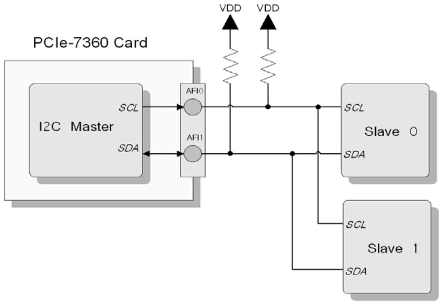
![The diagram illustrates an I2C communication setup involving a host card and two external slaves.\n\n**Blocks:**\n*   **PCIe-7360 Card**: A large container block encompassing the internal circuitry.\n*   **I2C Master**: Located inside the PCIe-7360 Card.\n*   **AFI0**: A vertical block containing a circle, located next to the I2C Master.\n*   **AFI1**: A vertical block containing a circle, located below AFI0.\n*   **Slave 0**: An external block on the right.\n*   **Slave 1**: An external block below Slave 0.\n\n**Connections:**\n*   **SCL**: A line labeled **SCL** originates from the **I2C Master** and points into **AFI0**. It then continues as a horizontal bus line connecting to **Slave 0** and **Slave 1** (both labeled **SCL**).\n*   **SDA**: A line labeled **SDA** originates from **AFI1** and points back into the **I2C Master**. It continues as a horizontal bus line connecting to **Slave 0** and **Slave 1** (both labeled **SDA**).\n*   **VDD**: Two zig-zag resistor symbols connect the top horizontal line (SCL) and bottom horizontal line (SDA) respectively to upward-pointing arrows labeled **VDD**.](.pcie-7360-50-11042-1000-200-en/a9ec667eb0890ba37528f9e2662ffded7559b41267cdb4e9544ce06d4e0d7d49.jpg)

Figure 3-29: I2C Master of PCIe-7360

The I $^{2}$ C master of the PCIe-7360 provides at most 8 bytes data width -- 4 bytes address/ command and 4 bytes data. A basic I $^{2}$ C command is consisted of at least two parts: slave address (with Read/Write bit) and one or more types of data bytes (Command,

Address or Data). Figure 3-29 shows the data transfer on the I $^{2}$ C bus.
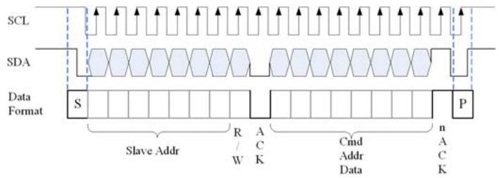
![SCL\nSDA\nData\nFormat\nS\nSlave Addr\nR / W\nA / C K\nCmd Addr Data\nP\nn A C K](.pcie-7360-50-11042-1000-200-en/30f36dfc842cb1780ddb784ecdb8d22b46d951ca754d82da1c239bdf90720ac0.jpg)

Figure 3-30: Data Transfer on the I²C Bus

$I^{2}C$ master of PCIe-7360 supports the clock range from 1.9 kHz to 244.14 kHz. After issuing command to $I^{2}C$ slave device, the clock rate might be changed according the request from $I^{2}C$ slave. The below formula is to calculate the $I^{2}C$ clock rate.

$$
F _ {s c l} = 4 8 8. 2 8 / (C l k P r e - s c a l e + 1) (k H z),
$$

$$
\text { where   Clk   Pre - scale } = 1 \text { to } 2 5 5
$$

I²C Write Command: the content of Cmd/Addr and Data are stored in registers I²C\_A\_CA and I²C\_A\_DAT and their byte counts are indicated by I²C CmdAddr Byte Count and Access Byte Count, respectively.
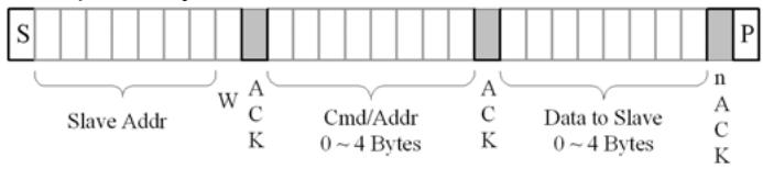
![S\nSlave Addr W A C K Cmd/Addr 0 ~ 4 Bytes A C K Data to Slave 0 ~ 4 Bytes n A C K P](.pcie-7360-50-11042-1000-200-en/3879c42980003e58dfa20b419b859b65fda2237b920414d8a3fd34f05d61ef90.jpg)

I²C Read Command: the format of Read command is similar with a write command except that the data part is derived by slave device.
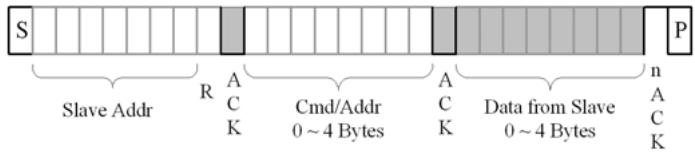
![S\nSlave Addr\nR\nA\nC\nK\nCmd/Addr\n0 ~ 4 Bytes\nA\nC\nK\nData from Slave\n0 ~ 4 Bytes\nn\nA\nC\nK\nP](.pcie-7360-50-11042-1000-200-en/82a8061b0311478cf47d345e0fea90a411532b1fd490a189e4ec53ade27ceeac.jpg)

I²C Cmd/Addr Count is less than 4 byte:
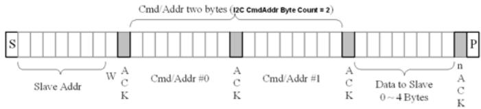
![S\nSlave Addr W A C K Cmd/Addr #0 A C K Cmd/Addr #1 A C K Data to Slave 0~4 Bytes n A C K P\nCmd/Addr two bytes (I2C CmdAddr Byte Count = 2)](.pcie-7360-50-11042-1000-200-en/01197f134d06dedf798ca4ad9cb8763f2a301a8a29445c0421cb1fe2cf4f86a4.jpg)

I²C Data Count is less than 4 byte:

![Data two bytes (12C Data Byte Count = 2)\nS\nSlave Addr W A C K Cmd/Addr 0 ~ 4 Bytes A C K Data #0 A C K Data #1 n A C K P\nA C K](.pcie-7360-50-11042-1000-200-en/dd1b216c90ee46aedcf316052e29c064172a12c1a31e27fdb94297e64e644f6d.jpg)

Figure 3-31: I²C Data Format

# SPI Master

PCIe-7360's application function I/O (AFI) can be configured as SPI node for user to communicate with peripheral devices through PCIe-7360's built-in SPI master protocol and provided API directly. Along with SPI master of PCIe-7360, user can easily communicate with ADC/ Microcontroller/ EEPROM/ image sensor for initializing and programming.

PCIe-7360 Card
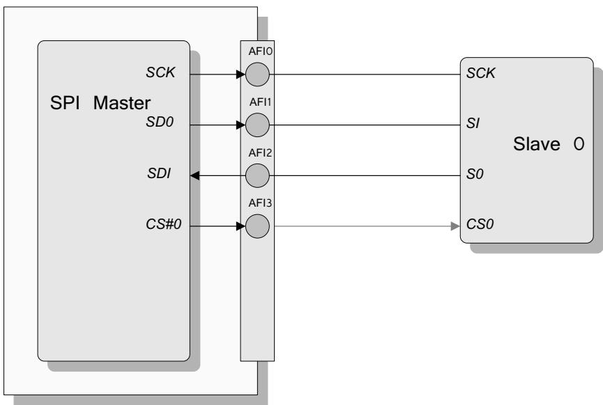
![The diagram illustrates a data flow between three main sections: an 'SPI Master' block on the left, a vertical strip labeled with 'AFI0', 'AFI1', 'AFI2', and 'AFI3' in the center, and a 'Slave 0' block on the right.\n\n**Connections:**\n*   **SPI Master to AFI Strip:**\n    *   An arrow connects 'SCK' on the 'SPI Master' block to the 'AFI0' label.\n    *   An arrow connects 'SD0' on the 'SPI Master' block to the 'AFI1' label.\n    *   An arrow originates from the 'AFI2' label and points to 'SDI' on the 'SPI Master' block.\n    *   An arrow connects 'CS#0' on the 'SPI Master' block to the 'AFI3' label.\n\n*   **AFI Strip to Slave 0:**\n    *   A line connects the 'AFI0' label to 'SCK' on the 'Slave 0' block.\n    *   A line connects the 'AFI1' label to 'SI' on the 'Slave 0' block.\n    *   A line connects the 'AFI2' label to 'SO' on the 'Slave 0' block.\n    *   An arrow connects the 'AFI3' label to 'CS0' on the 'Slave 0' block.](.pcie-7360-50-11042-1000-200-en/72da681d2fae51eb60cc3a80365b120e542107bf20c867c0955dbe6475490e4e.jpg)

Figure 3-32: SPI Master of PCIe-7360

SPI master of PCIe-7360 provide at most 64 bits -- 32 bits address/ command and 32 bits data. SPI master of PCIe-7360 supports only one slave device. Figure 3-32 shows the data transfer on SPI bus.
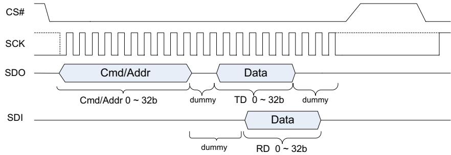
![The diagram illustrates a timing protocol involving four signals: **CS#**, **SCK**, **SDO**, and **SDI**.\n\n**Signals and Sequence:**\n\n*   **CS#**: A control signal that transitions from high to low to initiate the transaction and low to high to terminate it.\n*   **SCK**: A clock signal that pulses continuously while **CS#** is low.\n*   **SDO**: This line transmits a sequence of data blocks:\n    1.  A block labeled **'Cmd/Addr'** is shown above the text **'Cmd/Addr 0 ~ 32b'**.\n    2.  This is followed by a period labeled **'dummy'**.\n    3.  Next is a block labeled **'Data'** shown above the text **'TD 0 ~ 32b'**.\n    4.  This is followed by a final period labeled **'dummy'**.\n*   **SDI**: This line transmits a response sequence:\n    1.  A period labeled **'dummy'** (temporally aligned with the SDO 'dummy' period after TD).\n    2.  Followed by a block labeled **'Data'** shown above the text **'RD 0 ~ 32b'**.](.pcie-7360-50-11042-1000-200-en/741c93d29f2f665ac21a2dea5bcb7108fae5a3f5d4654a03110e373dd665264e.jpg)

Figure 3-33: Data Transfer on SPI Bus

SPI master of PCIe-7360 supports clock frequency range from 244.14 kHz to 62.5 MHz. After issuing command to SPI slave device, the clock rate might be changed according the request from SPI slave. The below formula is to calculate the SPI clock rate.

$$
\text { F   s   c   l } = 6 2. 5 / (\text { C   l   k   P   r   e   -   s   c   a   l   e } + 1) (\text { M   H   z }),
$$

$$
\text { where   Clk   Pre - scale } = 0 \text {   to   } 2 5 5
$$

SPI master of PCIe-7360 supports two different modes of SCK. Clock modes 0 and 1 of SCK are as shown.
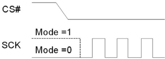
![CS#\nSCK\nMode =1\nMode =0](.pcie-7360-50-11042-1000-200-en/b3857881da40dbe37ad49a9abc8ab913d0f3304c99a0989840b4095cf2e7cb10.jpg)

Figure 3-34: Clock Mode of SCK

# External Digital Trigger

PCIe-7360 supports external digital trigger mode to start or pause an acquisition or generation operation. PCIe-7360 supports two trigger sources, internal software trigger and external digital trigger. The digital pattern acquisition or generation will start upon a software command or an external digital trigger signal to start or pause the process. The PCIe-7360's Application Function I/O (AFI) can be configured as the external digital trigger source.

PCIe-7360 Card
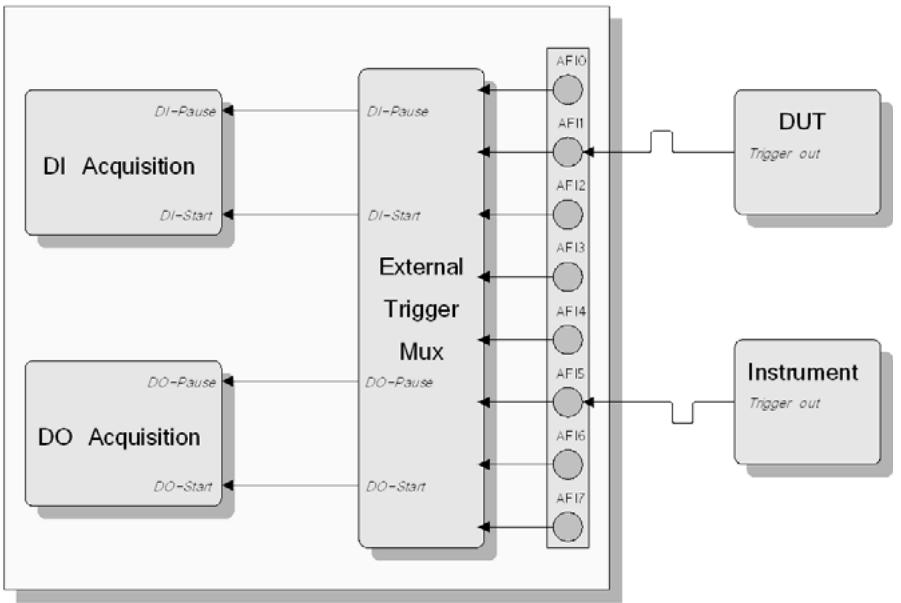
![**Labeled Blocks:**\n*   **DI Acquisition**\n*   **DO Acquisition**\n*   **External Trigger Mux**\n*   **AF10**, **AF11**, **AF12**, **AF13**, **AF14**, **AF15**, **AF16**, **AF17** (arranged vertically)\n*   **DUT** (with sub-label 'Trigger out')\n*   **Instrument** (with sub-label 'Trigger out')\n\n**Connections:**\n*   **DI Acquisition**: Connected to the **External Trigger Mux** via two lines labeled **DI-Pause** and **DI-Start**. Arrows point from the Mux to the DI Acquisition block.\n*   **DO Acquisition**: Connected to the **External Trigger Mux** via two lines labeled **DO-Pause** and **DO-Start**. Arrows point from the Mux to the DO Acquisition block.\n*   **AF10** through **AF17**: Connected to the **External Trigger Mux** via individual lines. Arrows point from the AF terminals into the External Trigger Mux.\n*   **DUT**: Connected to terminal **AF11** via a line labeled **Trigger out**. The arrow points towards AF11.\n*   **Instrument**: Connected to terminal **AF15** via a line labeled **Trigger out**. The arrow points towards AF15.](.pcie-7360-50-11042-1000-200-en/b093e2bdbc684b9639e66bc2b6f053f17795f9a15ec8400537f07d72bfc52524.jpg)

Figure 3-35: External Digital Trigger Input Configuration

# Trigger Out

PCIe-7360's Application Function I/O (AFI) can be configured as trigger output when receiving a software start command of digital pattern acquisition or generation. The trigger out signal can syn- chronize the operation between PCIe-7360 and DUT.

The pulse width of trigger out signal can be configured from 16ns to 524.288 $\mu$ s. (8 ns x (N+1), where N is from 1 to 65535)

PCIe-7360 Card
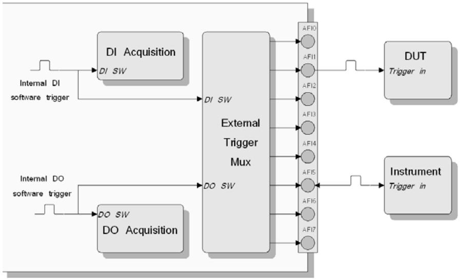
![Based on the provided image, here is an accurate and concise description of the flowchart:\n\n**Labeled Blocks:**\n*   **DI Acquisition** (contains the label 'DI SW')\n*   **DO Acquisition** (contains the label 'DO SW')\n*   **External Trigger Mux** (center block)\n*   **Vertical Strip** (labeled with circles: 'AF10', 'AF11', 'AF12', 'AF13', 'AF14', 'AF15', 'AF16', 'AF17')\n*   **DUT** (contains the label 'Trigger in')\n*   **Instrument** (contains the label 'Trigger in')\n\n**Connections:**\n*   **Inputs:**\n    *   'Internal DI software trigger' points to 'DI SW' in the 'DI Acquisition' block.\n    *   'Internal DO software trigger' points to 'DO SW' in the 'DO Acquisition' block.\n*   **To External Trigger Mux:**\n    *   An arrow labeled 'DI SW' connects 'DI Acquisition' to the 'External Trigger Mux'.\n    *   An arrow labeled 'DO SW' connects 'DO Acquisition' to the 'External Trigger Mux'.\n    *   A feedback loop connects the top of the 'External Trigger Mux' back to the 'DI SW' input of 'DI Acquisition'.\n    *   A feedback loop connects the bottom of the 'External Trigger Mux' back to the 'DO SW' input of 'DO Acquisition'.\n*   **From External Trigger Mux:**\n    *   Arrows connect the 'External Trigger Mux' to all circles on the vertical strip ('AF10' through 'AF17').\n*   **Outputs:**\n    *   From circle 'AF11', a line connects to 'DUT' (labeled 'Trigger in').\n    *   From circle 'AF15', a line connects to 'Instrument' (labeled 'Trigger in').](.pcie-7360-50-11042-1000-200-en/b632c53bd1f858adac904fae0d83459a0eaa4446aab5ac39ca23e199d30eae26.jpg)

Figure 3-36: Configured AFI as Internal Software Trigger Output

# Event Out

PCIe-7360's Application Function I/O (AFI) can be configured as event output of pattern match or COS (Change of State).

Pattern Match event is a pulse signal generated while the PCIe-7360's digital data input lines matching the pre-defined pattern. COS (Change of State) event is a pulse signal generated while the PCIe-7360 detects a change on the pre-defined data input line. The pulse width of Event Out signal can be configured from 16ns to 524.288 $\mu$ s. (8 ns x (N+1), where N is from 1 to 65535).

You can export this event out signal to trigger external devices for synchronization or to inform external devices.

PCIe-7360 Card
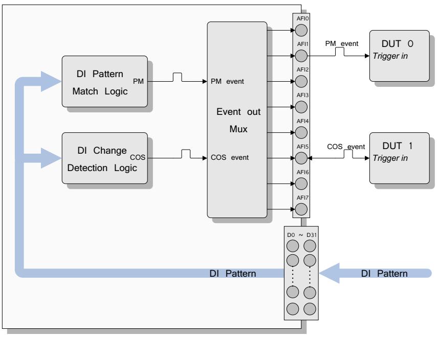
![Based on the provided image, here is the accurate and concise description of the flowchart:\n\n**Inputs and Logic Blocks**\n*   An arrow labeled **DI Pattern** enters from the right into a vertical block containing circles. Above this block is the label **D0 ~ D31**.\n*   From this bottom block, a thick light blue line labeled **DI Pattern** extends upward and splits into two arrows pointing left.\n*   The top arrow enters a block labeled **DI Pattern Match Logic**.\n*   The bottom arrow enters a block labeled **DI Change Detection Logic**.\n\n**Connections to Mux**\n*   From **DI Pattern Match Logic**, a small line labeled **PM** extends right and connects to a line labeled **PM event** entering the central block.\n*   From **DI Change Detection Logic**, a small line labeled **COS** extends right and connects to a line labeled **COS event** entering the central block.\n\n**Event out Mux and Outputs**\n*   The central vertical block is labeled **Event out Mux**. On its right side, there is a column of input circles labeled vertically from top to bottom: **AFI0**, **AFI1**, **AFI2**, **AFI3**, **AFI4**, **AFI5**, **AFI6**, **AFI7**.\n*   From the circle labeled **AFI0**, a line labeled **PM_event** extends right to a block labeled **DUT 0 Trigger in**.\n*   From the circle labeled **AFI5**, a line labeled **COS_event** extends right to a block labeled **DUT 1 Trigger in**.](.pcie-7360-50-11042-1000-200-en/3996a722141b621add91789eb775b8a7eb99c8c79fbdf1334c98325f1b58fdf2.jpg)

Figure 3-37: Pattern Match and COS Event Configuration

# Handshake

PCIe-7360's Application Function I/O (AFI) can be configured as handshake mode (DI-REQ/DI-ACK/DI-TRIG/DO-REQ/DO-ACK/DO-TRIG) to communicate with an external device using an acknowledge signals to request and acknowledge each data transfer. The handshake mode can ensure the data transfer without loss.

For the digital pattern acquisition using handshake, through DI-REQ input signal from external device and DI-ACK output signal to the external device, the digital input can have simple handshake data transfer. (See Section 3.7 Operating Modes)

For the digital pattern generation using handshake, through DO-REQ output signal to the external device and DO-ACK input signal from external device, the digital output can have simple handshake data transfer.

For the PCIe-7360 to communicate with peripheral devices using handshake, verify that the DUT and the PCIe-7360 have compatible timing.
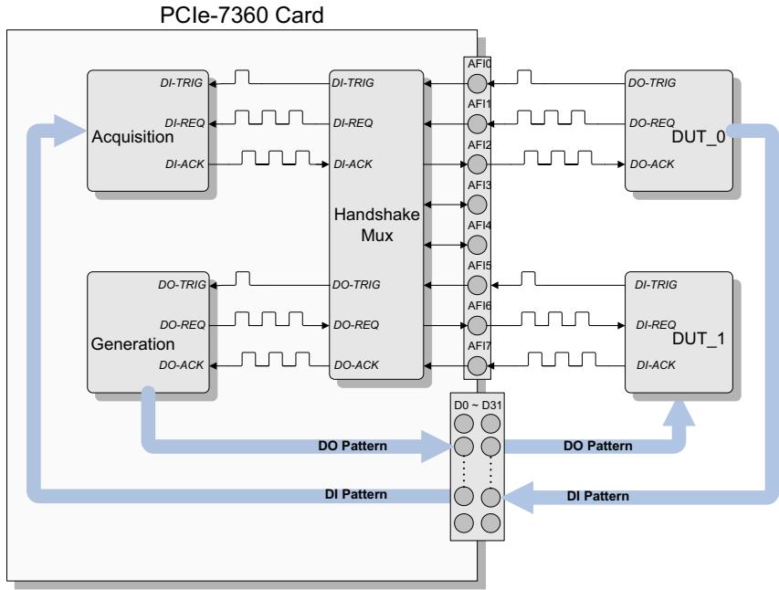
![The image displays a block diagram titled **PCIe-7360 Card**. It illustrates the signal flow between various components.\n\n**Blocks:**\n*   **Acquisition** (Top Left)\n*   **Generation** (Bottom Left)\n*   **Handshake Mux** (Center)\n*   **DUT_0** (Top Right)\n*   **DUT_1** (Bottom Right)\n*   **AFI** strip (Vertical column labeled **AFI0** through **AFI7**)\n*   **D0 ~ D31** (Bottom Center)\n\n**Connections:**\n\n**1. Acquisition and Handshake Mux:**\n*   **DI-TRIG:** Connected between Acquisition and Handshake Mux with an arrow pointing left (towards Acquisition).\n*   **DI-REQ:** Connected between Acquisition and Handshake Mux with an arrow pointing right (towards Handshake Mux).\n*   **DI-ACK:** Connected between Acquisition and Handshake Mux with an arrow pointing right (towards Handshake Mux).\n\n**2. Generation and Handshake Mux:**\n*   **DO-TRIG:** Connected between Generation and Handshake Mux with an arrow pointing left (towards Handshake Mux).\n*   **DO-REQ:** Connected between Generation and Handshake Mux with an arrow pointing right (towards Generation).\n*   **DO-ACK:** Connected between Generation and Handshake Mux with an arrow pointing right (towards Generation).\n\n**3. Handshake Mux and AFI Strip:**\n*   The top three lines (associated with **DI-TRIG**, **DI-REQ**, **DI-ACK**) connect the Handshake Mux to the AFI strip (**AFI0**, **AFI1**, **AFI2**) with arrows pointing left (towards Handshake Mux).\n*   The bottom three lines (associated with **DO-TRIG**, **DO-REQ**, **DO-ACK**) connect the Handshake Mux to the AFI strip (**AFI5**, **AFI6**, **AFI7**) with arrows pointing right (towards AFI strip).\n*   Two middle lines connect to **AFI3** and **AFI4** with arrows pointing left (towards Handshake Mux).\n\n**4. AFI Strip and DUTs:**\n*   **AFI0**, **AFI1**, **AFI2** connect to **DUT_0** (**DO-TRIG**, **DO-REQ**, **DO-ACK**) with arrows pointing left (towards AFI strip).\n*   **AFI5**, **AFI6**, **AFI7** connect to **DUT_1** (**DI-TRIG**, **DI-REQ**, **DI-ACK**) with arrows pointing right (towards DUT_1).\n\n**5. Data Pattern Connections (Blue Arrows):**\n*   From **Generation** to **D0 ~ D31**: Labeled **DO Pattern**.\n*   From **D0 ~ D31** to **DUT_1**: Labeled **DO Pattern**.\n*   From **D0 ~ D31** to **Acquisition**: Labeled **DI Pattern**.\n*   From **DUT_0** to **D0 ~ D31**: A blue arrow points left from DUT_0 to the D0 ~ D31 block.](.pcie-7360-50-11042-1000-200-en/abbed4659ad23586ca2ce24b7aecd3ccbab5a50cfa5f3c91e6d344a5de6c38a0.jpg)

Figure 3-38: Configured AFI as Handshake Interface

# Sample Clock In/Out

The AFI of PCIe-7360 can be configured to sample clock in/out pin. For more details, please see Section 3.6 Sample Clock

PCIe-7360 Card
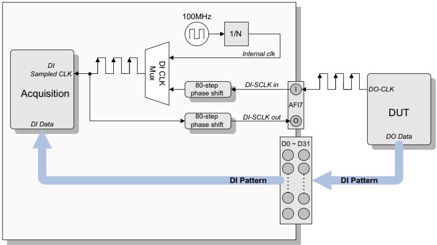
![The flowchart depicts a system with clock generation, phase shifting, multiplexing, and data acquisition paths.\n\n**Labeled Blocks:**\n*   **Acquisition** (contains 'DI Sampled CLK' and 'DI Data')\n*   **DI CLK Mux**\n*   **100MHz** (square wave icon)\n*   **1/N** (contains 'Internal clk')\n*   **80-step phase shift** (two blocks, top and bottom)\n*   **AFI7** (vertical block with '1' and '0')\n*   **DUT** (contains 'DO-CLK', 'DUT', 'DO Data')\n*   **D0 ~ D31** (vertical block with circles)\n\n**Connections:**\n*   **100MHz** connects to **1/N**.\n*   **1/N** connects to **DI CLK Mux** (labeled 'Internal clk').\n*   **AFI7** (port '1') connects to the top **80-step phase shift** block (labeled 'DI-SCLK in', arrow points left).\n*   **AFI7** (port '0') connects to the bottom **80-step phase shift** block (labeled 'DI-SCLK out', arrow points left).\n*   The top **80-step phase shift** block connects to **DI CLK Mux** (arrow points left).\n*   The bottom **80-step phase shift** block connects to **DI CLK Mux** (arrow points left).\n*   **DI CLK Mux** connects to **DI Sampled CLK** in the **Acquisition** block (sawtooth wave).\n*   **AFI7** connects to **DO-CLK** in the **DUT** block (sawtooth wave).\n*   **DO Data** in **DUT** connects to **D0 ~ D31** via a thick blue arrow (labeled 'DI Pattern').\n*   **D0 ~ D31** connects to **DI Data** in the **Acquisition** block via a thick blue arrow (labeled 'DI Pattern').](.pcie-7360-50-11042-1000-200-en/bf34541372a9681b0fa4dc2004b8024e675ba90b660e297a4345b09d1dd195a5.jpg)

Figure 3-39: Configured AFI7 as DI Sampled Clock In/Out

PCIe-7360 Card
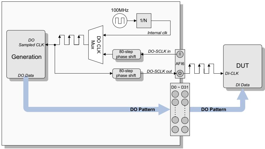
![Flowchart](.pcie-7360-50-11042-1000-200-en/c0a9742aa74905165fe80b4ac25c262d9eb08d3019fbe5e0c4a0af542f102a16.jpg)

Figure 3-40: Configured AFI6 as DO Sampled Clock In/Out

# 3.10 Pattern Match

PCIe-7360 supports pattern match function to monitor the data input lines that conform to the user-defined pattern (for example, 10101110). When the data lines conform to the user-defined pattern, PCIe-7360 will generate a pulse signal of pattern match event to the AFI pin and generate the pattern match interrupt to host PC as well.

Below are the conditions of pattern match. The pattern match can be a single change of specific data line or a combination of different data lines.

<table><tr><td>Logic State</td><td>Description</td></tr><tr><td>0</td><td>Match on a logic low level at the input channel</td></tr><tr><td>1</td><td>Match on a logic high level at the input channel</td></tr><tr><td>R</td><td>Match on rising edge at the input channel</td></tr><tr><td>F</td><td>Match on falling edge at the input channel</td></tr><tr><td>X</td><td>Ignore the input channel</td></tr></table>

An example of 9 channel (CH0 – CH8) pattern match operation is shown. All of the enabled DI channel's signal logic states is compared with the user-defined pattern "1100RRFFX". The pattern match event and interrupt is generated while the following conditions are all matched:

▶ CH0 and CH1 are logic high
▶ CH2 and CH3 are logic low
▶ CH4 and CH5 are rising edge
▶ CH6 and CH7 are falling edge
▶ CH8 is ignored

![The image displays a simple graphic icon of a piece of lined paper with a folded top-right corner. A large, thick red checkmark is overlaid diagonally across the document, extending from the bottom left towards the top right. The paper has horizontal black lines representing text or writing fields.](.pcie-7360-50-11042-1000-200-en/3a3a814e8df0413ea093c6f47bd7095a1a9b7b0ba2eb160808477daef20431cd.jpg)
NOTE:

In the PCIe-7360, edge detection (rising or falling) compares currently sampled data with the previously sampled data.

![The image is a timing diagram illustrating a 'Sampled clock' at the top, which is a square wave. Below this are two columns labeled 'Use-defined pattern' and 'Enabled CH'.\n\nThe rows display waveforms for channels CH0 through CH8, corresponding to specific patterns listed in the left column:\n*   **CH0 (Pattern 1):** A square wave starting at the first rising edge of the clock.\n*   **CH1 (Pattern 1):** A square wave starting at the second rising edge.\n*   **CH2 (Pattern 0):** A square wave starting at the third rising edge.\n*   **CH3 (Pattern 0):** A square wave starting at the fourth rising edge.\n*   **CH4 (Pattern R):** A signal that rises at the first clock edge, indicated by an upward-pointing arrow.\n*   **CH5 (Pattern R):** A signal that rises at the third clock edge, indicated by an upward-pointing arrow.\n*   **CH6 (Pattern F):** A signal that goes high and then low, with a downward-pointing arrow on the falling edge.\n*   **CH7 (Pattern F):** A signal that goes high and then low, with a downward-pointing arrow on the falling edge.\n*   **CH8 (Pattern X):** A square wave.\n\nTwo vertical grey lines extend downwards from the first and third rising edges of the 'Sampled clock'. At the bottom, two final signals are shown:\n*   **PM Match Event:** A signal that goes high at the times indicated by the vertical lines.\n*   **PM Match Interrupt:** Narrow pulses that occur at the same times as the 'PM Match Event' goes high.](.pcie-7360-50-11042-1000-200-en/33357f27514e46bbea69b9eb0253b9bd80f68b6e25f124dc835f9d9ce8dede2c.jpg)
Figure 3-41: Example of Pattern Matching

# 3.11 COS (Change of State) Event

PCIe-7360 supports COS (Change of State) Event to monitor if there is any change on the user-defined or any data lines.

When PCIe-7360 detects the change (either the input state changes from low to high or from high to low) of data input lines, PCIe-7360 will have the following response:

▶ Generate a pulse signal of change detection event to AFI
▶ Generate the change detection interrupt to host PC
▶ Latch the corresponding DI data into change detection latch register

In COS mode, the DI data are sampled by 125 MHz clock rate. Therefore, the pulse width of the DI data should be longer than 8ns. Otherwise, the change detection latch register won't latch the correct input data.

An example of 8 channel change detection operation is shown. Any level change of the enabled DI data lines is detected and then generate the event and interrupt. The corresponding DI data is latched into change detection register.

![Flowchart](.pcie-7360-50-11042-1000-200-en/401dd4202c271cbc6f1dd10a1ab52836498618617fd1fcb47432e8c186491d6e.jpg)

Figure 3-42: Example of Pattern Match

# 3.12 Termination

Proper termination is very important for applications using high-speed digital data transfer to eliminate the signal reflection caused by cables, wiring, connectors, or PCB traces and improve signal quality.

The output impedance (source impedance) of the PCIe-7360 is 50 Ω and the characteristic impedance of the SCSI-VHDCI cable is also 50 Ω. When you connect to a DUT with 50 Ω input impedance, the best impedance matching is achieved, but the voltage level sensed by the DUT is half of the PCI-7360's output voltage due to voltage-divider principles. You can also connect to a DUT with a high impedance (at least 1 - 100 kΩ) if precision timing and excellent signal integrity is not so critical. The voltage level sensed by the DUT is almost the same as the output voltage of the PCIe-7360.

The input impedance of the PCIe-7360 is 10 kΩ, which is a high impedance. So with a high impedance 10 kΩ load termination, the external source impedance of DUT should match the characteristic impedance (50 Ω) of the SCSI-VHDCI cable to achieve better signal integrity and avoid signal reflection.

This page intentionally left blank.

# Appendix A ADLINK DIN-68H

The DIN-68H is a terminal board designed for PCIe-7360 to provide the easier wiring for test circuit or measure signal. Below is the layout and pin-to-pin reference table of DIN-68H:

![T83\nn-5Vdc\nGNV\nD0-D2L Termination\nFull Clean\nFull U-p\nD0J\nD1N-69H\n51-14068-0A10\nI/O Bus\nI/O Bus\nI/O Bus\nI/O Bus\nI/O Bus\nI/O Bus\nI/O Bus\nI/O Bus\nI/O Bus\nI/O Bus\nI/O Bus\nI/O Bus\nI/O Bus\nI/O Bus\nI/O Bus\nI/O Bus\nI/O Bus\nI/O Bus\nI/O Bus\nI/O Bus\nI/O Bus\nI/O Bus\nI/O Bus\nI/O Bus\nI/O Bus\nI/O B13 D30 B14 D36 D37 D38 D39 D40 D41 D42 D43 D44 D45 D46 D47 D48 D49 D50 D51 D52 D53 D54 D55 D56 D57 D58 D59 D60 D61 D62 D63 D64 D65 D66 D67 D68 D69 D70 D71 D72 D73 D74 D75 D76 D77 D78 D79 D80 D81 D82 D83 D84 D85 D86 D87 D88 D89 D90 D91 D92 D93 D94 D95 D96 D97 D98 D99 D100 D101 D102 D103 D104 D105 D106 D107 D108 D109 D110 D111 D112 D113 D114 D115 D116 D117 D118 D119 D120 D121 D122 D123 D124 D125 D126 D127 D128 D129 D130 D131 D132 D133 D134 D135 D136 D137 D138 D139 D140 D141 D142 D143 D144 D145 D146 D147 D148 D149 D150 D151 D152 D153 D154 D155 D156 D157 D158 D159 D160 D161 D162 D163 D164 D165 D166 D167 D168 D169 D170 D171 D172 D173 D174 D175 D176 D177 D178 D179 D180 D181 D182 D183 D184 D185 D186 D187 D188 D189 D190 D191 D192\nI/O Bus\nI/O Bus\nI/O Bus\nI/O Bus\nI/O Bus\nI/O Bus\nI/O Bus\nI/O Bus\nI/O Bus\nI/O Bus\nI/O Bus\nI/O Bus\nI/O Bus\nI/O Bus\nI/O Bus\nI/O Bus\nI/O Bus\nI/O Bus\nI/O Bus\nI/O Bus\nI/O Bus\nI/O Bus\nI/O Bus\nI/O Bus\nI/Obus\nI/Obus\nT82](.pcie-7360-50-11042-1000-200-en/da634dd1f3197b3c08380c86df32cf4afd98d6c32ff62b3661fe7db6c124cf0e.jpg)

Figure A-1: DIN-68H Layout

<table><tr><td>PCIe-7360</td><td>DI/O0</td><td>DI/O1</td><td>DI/O2</td><td>DI/O3</td><td>DI/O4</td><td>DI/O5</td><td>DI/O6</td><td>DI/O7</td></tr><tr><td>DIN-68H</td><td>D0</td><td>D1</td><td>D2</td><td>D3</td><td>D4</td><td>D5</td><td>D6</td><td>D7</td></tr></table>

<table><tr><td>PCIe-7360</td><td>DI/O8</td><td>DI/O9</td><td>DI/O10</td><td>DI/O11</td><td>DI/O12</td><td>DI/O13</td><td>DI/O14</td><td>DI/O15</td></tr><tr><td>DIN-68H</td><td>D8</td><td>D9</td><td>D10</td><td>D11</td><td>D12</td><td>D13</td><td>D14</td><td>D15</td></tr></table>

<table><tr><td>PCIe-7360</td><td>DI/O16</td><td>DI/O17</td><td>DI/O18</td><td>DI/O19</td><td>DI/O20</td><td>DI/O21</td><td>DI/O22</td><td>DI/O23</td></tr><tr><td>DIN-68H</td><td>D16</td><td>D17</td><td>D18</td><td>D19</td><td>D20</td><td>D21</td><td>D22</td><td>D23</td></tr></table>

<table><tr><td>PCIe-7360</td><td>DI/O24</td><td>DI/O25</td><td>DI/O26</td><td>DI/O27</td><td>DI/O28</td><td>DI/O29</td><td>DI/O30</td><td>DI/O31</td></tr><tr><td>DIN-68H</td><td>D24</td><td>D25</td><td>D26</td><td>D27</td><td>D28</td><td>D29</td><td>D30</td><td>D31</td></tr></table>

<table><tr><td>PCIe-7360</td><td>AFI6</td><td>AFI7</td></tr><tr><td>DIN-68H</td><td>AF6</td><td>AF7</td></tr></table>

Table A-1: DIN-68H Pin Assignment

All jumpers on DIN-68H are used for the setting of pull-up or pull-down resistor termination. The proper termination setting can reduce signal reflection during high-speed data transfer. The below diagram is the schematic of AF6, AF7, and D0 to D31. The default jumper setting of DIN-68H is set to 50Ω pull-down termination. When you change the jumper setting to 5V pull-up termination, you have to apply +5V power to +5V $_{IN}$ connector. If you don't want to set termination on specific channels, just remove the corresponding jumpers on the DIN-68H..

![D0 - D31 AF6 - AF7\nJumper\n50 User define\n10K\n+5Vdc\nJumper\nUser define\n50\nD0 - D31 AF6 - AF7](.pcie-7360-50-11042-1000-200-en/6509794f1d50c5c1a0f6a26f32fa56b1b6583fb146e699dd530708bd08350dee.jpg)

Figure A-2: Resistor Termination Schematic

The DIN-68H also provides the option of user define pull-up resistor termination. Please note that the pad position of the resistor is on the back side of PCB and the resistor footprint is 1206 packaging. Below is the layout of the back side PCB and reference table of user-defined resistor termination.

<table><tr><td>Channel</td><td>D0</td><td>D1</td><td>D2</td><td>D3</td><td>D4</td><td>D5</td><td>D6</td><td>D7</td></tr><tr><td>Resistor</td><td>R71</td><td>R72</td><td>R79</td><td>R80</td><td>R87</td><td>R88</td><td>R97</td><td>R98</td></tr></table>

<table><tr><td>PCIe-7360</td><td>D8</td><td>D9</td><td>D10</td><td>D11</td><td>D12</td><td>D13</td><td>D14</td><td>D15</td></tr><tr><td>DIN-68H</td><td>R73</td><td>R74</td><td>R81</td><td>R82</td><td>R89</td><td>R90</td><td>R99</td><td>R100</td></tr></table>

<table><tr><td>PCIe-7360</td><td>D16</td><td>D17</td><td>D18</td><td>D19</td><td>D20</td><td>D21</td><td>D22</td><td>D23</td></tr><tr><td>DIN-68H</td><td>R75</td><td>R76</td><td>R83</td><td>R84</td><td>R91</td><td>R92</td><td>R101</td><td>R102</td></tr></table>

<table><tr><td>PCIe-7360</td><td>D24</td><td>D25</td><td>D26</td><td>D27</td><td>D28</td><td>D29</td><td>D30</td><td>D31</td></tr><tr><td>DIN-68H</td><td>R77</td><td>R78</td><td>R85</td><td>R86</td><td>R93</td><td>R94</td><td>R103</td><td>R104</td></tr></table>

<table><tr><td>PCIe-7360</td><td>AF6</td><td>AF7</td></tr><tr><td>DIN-68H</td><td>R95</td><td>R96</td></tr></table>

Table A-2: Pad Position of User-Defined Resistor Termination

![L3\nC3\nL4\nC4\nC2\nD\nD1\nR3\nR2\nL1\nR1 R4\nP7 P37 P29 P45 P87 P53 P92 P63 P72 P39 P81 P41 P89 P56 P98 P65 P75 P41 P82 P49 P91 P52 P108 P62 P77 P43 P85 P51 P93 P58 P103 P89\nP86\nP25 P61 P77 P23 P9\nP24 P60 P45 P88 P54 P88 P64 P24 P49 P87 P48 P90 P56 R109 P66 R76 R42 P84 P59 P92 P58 R104 P68 R78 R48 P86 P52 P90 P56 R104 F70\nP23\nP22\nP21\nP20\nP19\nP18\nP17\nP16\nP15\nP14\nP13\nP12\nP11\nP10\nP9\nP8\nP7\nP6\nP5\nP4\nP3\nP2\nP1\nP0\nP9\nP8\nP7\nP6\nP5\nP4\nP3\nP2\nP1\nP0\nP9\nP8\nP7\nP6\nP5\nP4\nP3\nP2\nP1\nP0](.pcie-7360-50-11042-1000-200-en/3978bbd828fbc24eec195307505a8f435f10881478d0ee7dcabcc829eeb7c0f9.jpg)

Figure A-3: DIN-68H Layout (Back Side)

This page intentionally left blank.

# Important Safety Instructions

For user safety, please read and follow all instructions, WARNINGS, CAUTIONS, and NOTES marked in this manual and on the associated equipment before handling/operating the equipment.

▶ Read these safety instructions carefully.
- Keep this user’s manual for future reference.
▶ Read the specifications section of this manual for detailed information on the operating environment of this equipment.
- When installing/mounting or uninstalling/removing equipment:

▷ Turn off power and unplug any power cords/cables.

▶ To avoid electrical shock and/or damage to equipment:

▷ Keep equipment away from water or liquid sources;
▷ Keep equipment away from high heat or high humidity;
▷ Keep equipment properly ventilated (do not block or cover ventilation openings);

▶ Make sure to use recommended voltage and power source settings;

▶ Always install and operate equipment near an easily accessible electrical socket-outlet;

▷ Secure the power cord (do not place any object on/over the power cord);

▶ Only install/attach and operate equipment on stable surfaces and/or recommended mountings; and,

▷ If the equipment will not be used for long periods of time, turn off and unplug the equipment from its power source.

▶ Never attempt to fix the equipment. Equipment should only be serviced by qualified personnel.

A Lithium-type battery may be provided for uninterrupted, backup or emergency power.

![The image displays a standard safety sign featuring a red triangle containing a white exclamation point in the center. Directly below the triangle, the word 'WARNING' is printed in black, bold, capital letters on a white background.](.pcie-7360-50-11042-1000-200-en/1f67064580548b1f46194ce72719dab9d8e041b23024c7fdf8cf3c41a86fb77c.jpg)

Risk of explosion if battery is replaced with one of an incorrect type. Dispose of used batteries appropriately.

▶ Equipment must be serviced by authorized technicians when:

The power cord or plug is damaged;
▷ Liquid has penetrated the equipment;
It has been exposed to high humidity/moisture;
$\triangleright$ It is not functioning or does not function according to the user's manual;
▷ It has been dropped and/or damaged; and/or,
▷ It has an obvious sign of breakage.

# Getting Service

Contact us should you require any service or assistance.

# ADLINK Technology, Inc.

Address: 9F, No.166 Jian Yi Road, Zhonghe District
New Taipei City 235, Taiwan
新北市中和區建一路 166 號 9 樓

Tel: +886-2-8226-5877

Fax: +886-2-8226-5717

Email: service@adlinktech.com

# Ampro ADLINK Technology, Inc.

Address: 5215 Hellyer Avenue, #110, San Jose, CA 95138, USA

Tel: +1-408-360-0200

Toll Free: +1-800-966-5200 (USA only)

Fax: +1-408-360-0222

Email: info@adlinktech.com

# ADLINK Technology (China) Co., Ltd.

Address: 上海市浦东新区张江高科技园区芳春路 300 号 (201203)
300 Fang Chun Rd., Zhangjiang Hi-Tech Park,
Pudong New Area, Shanghai, 201203 China

Tel: +86-21-5132-8988

Fax: +86-21-5132-3588

Email: market@adlinktech.com

# ADLINK Technology Beijing

Address: 北京市海淀区上地东路 1 号盈创动力大厦 E 座 801 室(100085)
Rm. 801, Power Creative E, No. 1,
Shang Di East Rd., Beijing, 100085 China

Tel: +86-10-5885-8666

Fax: +86-10-5885-8626

Email: market@adlinktech.com

# ADLINK Technology Shenzhen

Address: 深圳市南山区科技园南区高新南七道 数字技术园

A1 栋 2 楼 C 区 (518057)

2F, C Block, Bldg. A1, Cyber-Tech Zone, Gao Xin Ave. Sec. 7, High-Tech Industrial Park S., Shenzhen, 518054 China

Tel: +86-755-2643-4858

Fax: +86-755-2664-6353

Email: market@adlinktech.com

# LiPPERT ADLINK Technology GmbH

Address: Hans-Thoma-Strasse 11, D-68163, Mannheim, Germany

Tel: +49-621-43214-0

Fax: +49-621 43214-30

Email: emea@adlinktech.com

# ADLINK Technology, Inc. (French Liaison Office)

Address: 15 rue Emile Baudot, 91300 Massy CEDEX, France

Tel: +33 (0) 1 60 12 35 66

Fax: +33 (0) 1 60 12 35 66

Email: france@adlinktech.com

# ADLINK Technology Japan Corporation

Address: 〒101-0045 東京都千代田区神田鍛冶町 3-7-4
神田 374 ビル 4F
KANDA374 Bldg. 4F, 3-7-4 Kanda Kajicho,
Chiyoda-ku, Tokyo 101-0045, Japan

Tel: +81-3-4455-3722

Fax: +81-3-5209-6013

Email: japan@adlinktech.com

# ADLINK Technology, Inc. (Korean Liaison Office)

Address: 서울시 서초구 서초동 1675-12 모인터빌딩 8 층 8F Mointer B/D,1675-12, Seocho-Dong, Seocho-Gu, Seoul 137-070, Korea

Tel: +82-2-2057-0565

Fax: +82-2-2057-0563

Email: korea@adlinktech.com

# ADLINK Technology Singapore Pte. Ltd.

Address: 84 Genting Lane #07-02A, Cityneon Design Centre, Singapore 349584

Tel: +65-6844-2261

Fax: +65-6844-2263

Email: singapore@adlinktech.com

# ADLINK Technology Singapore Pte. Ltd. (Indian Liaison Office)

Address: 1st Floor, #50-56 (Between 16th/17th Cross) Margosa Plaza, Margosa Main Road, Malleswaram, Bangalore-560055, India

Tel: +91-80-65605817, +91-80-42246107

Fax: +91-80-23464606

Email: india@adlinktech.com

# ADLINK Technology, Inc. (Israeli Liaison Office)

Address: 6 Hasadna St., Kfar Saba 44424, Israel

Tel: +972-9-7446541

Fax: +972-9-7446542

Email: israel@adlinktech.com