# PCIe-7856/7853

# Master-Slave Distributed Motion and I/O Master Controller

# User’s Manual

![Green PCIe-7856 dual-chip network card with visible circuitry and port labels (no readable text beyond branding)](.pcie-7856-53-50-15113-1010-11/e0014f2b982ab0639b19307c64ad77b6402d5da926e75e934c51fea29fa0e7ab.jpg)

![Green PCIe 7853 microcontroller board with visible ports and components (no readable text or symbols beyond branding)](.pcie-7856-53-50-15113-1010-11/c54219faa315b1288b27e0acff8ea173672720817dd12b73a9cb8ae6a833fb3e.jpg)

Manual Rev.: 1.1

Revision Date: Sept. 17, 2020

Part No: 50-15113-1010

Revision History

<table><tr><td>Revision</td><td>Release Date</td><td>Description of Change(s)</td></tr><tr><td>1.0</td><td>2020-02-27</td><td>Initial release</td></tr><tr><td>1.1</td><td>2020-09-17</td><td>Add PCIe-7853; integrate HSL System documentation</td></tr></table>

# Preface

# Copyright © 2020 ADLINK Technology Inc.

This document contains proprietary information protected by copyright. All rights are reserved. No part of this manual may be reproduced by any mechanical, electronic, or other means in any form without prior written permission of the manufacturer.

# Disclaimer

The information in this document is subject to change without prior notice in order to improve reliability, design, and function and does not represent a commitment on the part of the manufacturer.

In no event will the manufacturer be liable for direct, indirect, special, incidental, or consequential damages arising out of the use or inability to use the product or documentation, even if advised of the possibility of such damages.

# Environmental

ADLINK is committed to fulfill its social responsibility to global environmental preservation through compliance with the European Union's Restriction of Hazardous Substances (RoHS) directive and Waste Electrical and Electronic Equipment (WEEE) directive. Environmental protection is a top priority for ADLINK. We have enforced measures to ensure that our products, manufacturing processes, components, and raw materials have as little impact on the environment as possible. When products are at their end of life, our customers are encouraged to dispose of them in accordance with the product disposal and/or recovery programs prescribed by their nation or company.

![Symbol of a trash bin crossed with a diagonal line and a horizontal bar below (no text or labels)](.pcie-7856-53-50-15113-1010-11/6f151e5aa52e38f341335f559d6b16d463febc4a8e7a573a1ec612ba6b14416e.jpg)

# Battery Labels (for products with battery)

![Symbol of a trash bin crossed out by two diagonal lines (no text or numbers present)](.pcie-7856-53-50-15113-1010-11/887b4ba7054e97b74c0b320e90c9a51b4fb5030742672b3cb10c84bfb8e2030f.jpg)

![Simple line drawing of a recycling symbol (three chasing arrows) inside a square frame, no text or labels present.](.pcie-7856-53-50-15113-1010-11/d36d13b35960c4442ffdb9be51e7d20f8aa053ac3bf3c7b244003eb48b57f494.jpg)

Li-ion

![RECYCLE\nRBRC\nLi-ion\n1.800.822.8837](.pcie-7856-53-50-15113-1010-11/a6a37128b1397c293b36cffe254afffd6a78b0d8ffc14e60e29ebd0b3824efcf.jpg)

![Abstract geometric pattern with interlocking X and Y shapes (no text or symbols)](.pcie-7856-53-50-15113-1010-11/3b37d389c9723c049d4da15e968e11303abd27a4c631125fdda6e54e48643766.jpg)

ᘄ㟁ụㄳᅇᨲ

# California Proposition 65 Warning

![A yellow triangular warning sign with a thick black border containing a black exclamation point in the center, set against a white background.](.pcie-7856-53-50-15113-1010-11/41f8afdc6b148853c627ed1733348177dc33491e59e677f13a1c6199bf45499c.jpg)

WARNING: This product can expose you to chemicals including acrylamide, arsenic, benzene, cadmium, Tris(1,3-dichloro-2-propyl)phosphate (TDCPP), 1,4-Dioxane, formaldehyde, lead, DEHP, styrene, DINP, BBP, PVC, and vinyl materials, which are known to the State of California to cause cancer, and acrylamide, benzene, cadmium, lead, mercury, phthalates, toluene, DEHP, DIDP, DnHP, DBP, BBP, PVC, and vinyl materials, which are known to the State of California to cause birth defects or other reproductive harm. For more information go to www.P65Warnings.ca.gov.

# Trademarks

Product names mentioned herein are used for identification purposes only and may be trademarks and/or registered trademarks of their respective companies.

# Conventions

Take note of the following conventions used throughout this manual to make sure that users perform certain tasks and instructions properly.

![The image displays a white document icon with a folded top-right corner and horizontal lines representing text. Overlaid on the document is a large, red checkmark.](.pcie-7856-53-50-15113-1010-11/60a0d359ddd74a1667eac0f6a53cd518f5e38b33b3e11cf433abe17164206507.jpg)
NOTE:

Additional information, aids, and tips that help users perform tasks.

![The image displays a standard warning sign consisting of a yellow triangle with a thick black border. Centered inside the triangle is a large, black exclamation mark.](.pcie-7856-53-50-15113-1010-11/b21e0090477b771b1704b5ef640f3261b778f577e3e53f87bdb777f6e6b500ea.jpg)
CAUTION:

Information to prevent minor physical injury, component damage, data loss, and/or program corruption when trying to complete a task.

![A standard warning symbol featuring a red triangle with a white border and a white exclamation point in the center.](.pcie-7856-53-50-15113-1010-11/d7496c4cea03e62cc2608bd924517c1371b6990d36c2a444f6bdf4f9a7fbe3c9.jpg)
WARNING:

Information to prevent serious physical injury, component damage, data loss, and/or program corruption when trying to complete a specific task.

# Table of Contents

# Preface ......... iii

# List of Figures ......... ix

# List of Tables ......... .... xi

# 1 Introduction ........

1.1 Specifications... 3
1.2 Supported Software . 4

# 2 Installation ........ 5

2.1 Package Contents .... 5
2.2 PCIe-7856 Mechanical Drawing . 6
2.3 Driver Installation ... 7

2.3.1 PCIe-7856 . 7
2.3.2 PCIe-7853 . 7

2.4 Troubleshooting ...... 7
2.5 Signal Connections...... 7

2.5.1 Connecting HSL/MNET Slave Modules.... 8
2.5.2 RJ45 Pin Assignments .... 9
2.5.3 HSL and Motionnet LED Indicators .... .. 10

2.6 SW1 Card ID Switch Settings ..... 11

# 3 MNET Master-Slave Motion System ................ 1 3

3.1 MNET System Specifications .... 1 4

3.1.1 Wiring Cables ..... .. 15
3.1.2 MNET System Communication . .. 16

3.2 MNET Motion Modules . 18

3.2.1 Motion Module Mechanical Drawings. .. 20

# 4 HSL Slave Modules ....... 23

# 4.1 HSL Slave I/O Modules... . 24

4.1.1 Discrete I/O Module .. ... 24
4.1.2 Analog I/O Modules ..... .... 25

# 4.2 General Specifications.... . 26

4.2.1 Digital I/O Modules .... ... 26
4.2.2 Analog I/O Modules ..... .. 27
4.2.3 HSL Module DIP Switch .. 28
4.2.4 Daughter Board/Module Dimensions.......... ... 29
4.2.5 Wiring Diagrams ...... ... 32
4.2.6 Terminal Base Motion Control Modules..... ... 36
4.2.7 Managing Slave Indexes in an HSL Network ........... 43

# 5 MotionCreatorPro 2 (MCP2) .......... . 47

5.1 About MCP2.. . 47
5.2 How to Run MCP2 .. . 47
5.3 MCP2 Features.... . 48

5.3.1 Main Menu ..... .. 48
5.3.2 HSL Distributed I/O Manager... .. 51
5.3.3 MNET Distributed Motion Manager ..... .. 53

# 5.4 MCP2 Error Codes... 62

# 6 Scan Time Table........ ....... 63

# 6.1 Full-duplex Mode .... 63

# 7 HSL LinkMaster Utility......... ..... 65

7.1 Software Installation.. 66
7.2 ADLINK HSL LinkMaster Utility..... 67

# 8 HSL Function Library ........ . 73

8.1 List of Functions... 73
8.2 Initialization and System Information ... . 76
8.3 Error Codes... . 81
8.4 Timer Control ... . 84

8.5 Discrete I/O ... . 87
8.6 Analog I/O ...... 96

# 9 How to Program with HSL Function Library................ 103

9.1 Programming with HSL DLL .. . 103

# Important Safety Instructions ......... . 107

# Getting Service........ . 109

This page intentionally left blank.

# List of Figures

Figure 1-1: PCIe-7856 Block Diagram . 2

Figure 2-1: PCIe-7856 Mechanical Drawing .. 6

Figure 2-2: LED Indicators on the PCIe-7856.. . 10

Figure 3-1: MNET Distributed Motion Control System.. . 13

Figure 3-2: MNET System Communication Sequence ............. .. 17

Figure 3-3: MNET-MIA with MINAS A4 Servo Driver.. .. 20

Figure 3-4: MNET-4XMO-(C) Mechanical Diagram .. .. 21

Figure 4-1: HSL Module DIP Switch Location.. . 28

Figure 8-1: Type 1... .. 89

Figure 8-2: Type 2.. .. 89

Figure 8-3: Type 3... .. 90

Figure 9-1: Programming Flow.. . 103

This page intentionally left blank.

# List of Tables

Table 3-1: MNET System Specifications . . 14
Table 3-2: MNET Motion Module Series.. . 18
Table 4-1: HSL Discrete I/O Module Series. . 24
Table 4-2: HSL Discrete I/O Module Selection Guide.. . 24
Table 4-3: HSL Analog I/O Module Series. .. 25
Table 4-4: HSL Analog I/O Module Selection Guide... .. 25
Table 4-5: Digital I/O Module . .. 26
Table 4-6: Analog I/O Modules .. . 27

This page intentionally left blank.

# 1 Introduction

As industrial machine automation continues to advance, designers require not only centralized control systems but also distributed solutions to develop more complex machine applications. Distributed solutions provide many benefits such as lower maintenance, reduced wiring, and easy integration of vast numbers of modules. Motionnet (MNET) and High Speed Link (HSL) are innovative distributed motion and I/O technologies that enable time-deterministic scanning of thousands of I/O points within milliseconds using the master-slave architecture. The MNET bus further improves distributed motion control capability by providing control of up to 256 axes plus minimal command execution time for single-axis control.

The PCIe-7856 is a PCI Express interface card with two ports for MNET and HSL systems for distributed motion and I/O modules for a wide variety of machine automation applications.

HSL technology allows thousands of I/O points to be scanned at the millisecond level in real time by means of the master-slave architecture. Commercial Ethernet cables with RJ45 connectors are used for simplified setup of HSL slave modules as close as possible to sensor devices, resulting in dramatic wiring reduction. System integrators can greatly benefit from an HSL network because it integrates discrete I/O and analog I/O modules. This local network features rapid-response, real-time scanning.

An MNET system is a distributed motion solution for machine systems. MNET is an innovative distributed motion technology which provides distributed motion axis control of up to 256 axes for any servo/stepper motor controlled using mater-slave architecture. This not only facilitates general purpose 4-axis motion control, but also allows up to 64 specific single-axis motion control modules to be scanned at the millisecond level in real time.

# MNET and HSL features:

 Flexible, comprehensive, extendable distributed motion and I/O solution based on PC architecture or embedded platform.
 Convenient wiring for remote distributed motion and I/O modules, inc. multiple-axis motion control modules, singleaxis motion control modules, discrete I/Os, and analog I/Os.
 Saves space, reduces wiring, and lowers costs due to ease of maintenance.
Fast, time-deterministic scanning with hundreds of discrete I/O points (up to 2,016 points).
 Rapid, real-time scanning to support high-speed and highresponse motion control of up to 256 axes.

The PCIe-7856 block diagram is as follows.

![Based on the provided diagram, here are the labeled blocks and their connections:\n\n**Labeled Blocks:**\n*   FPGA\n*   Motionnet Master Controller\n*   HSL Master Controller\n*   FRAM\n*   MNET Transceiver IF Circuit\n*   HSL Transceiver IF Circuit\n*   MRJ45\n*   HRJ45\n*   PCI BUS\n*   Motionnet Topology\n*   HSL Topology\n\n**Connections:**\n*   **FPGA** connects via a single arrow to the **Motionnet Master Controller**.\n*   **FPGA** connects via a single arrow to the **HSL Master Controller**.\n*   **FPGA** connects via an L-shaped single arrow to the **FRAM**.\n*   **FPGA** connects via a double-headed vertical arrow to the **PCI BUS**.\n*   **Motionnet Master Controller** connects via a double-headed horizontal arrow to the **MNET Transceiver IF Circuit**.\n*   **MNET Transceiver IF Circuit** connects via a double-headed horizontal arrow to the **MRJ45**.\n*   **HSL Master Controller** connects via a double-headed horizontal arrow to the **HSL Transceiver IF Circuit**.\n*   **HSL Transceiver IF Circuit** connects via a double-headed horizontal arrow to the **HRJ45**.\n*   The **MRJ45** block is connected to a chain of loops labeled **Motionnet Topology**.\n*   The **HRJ45** block is connected to a chain of loops labeled **HSL Topology**.](.pcie-7856-53-50-15113-1010-11/6fb21279df5a05f218ef21a2c9dc9e46420b3f7763310c02df9f17ddfb7d3b36.jpg)

Figure 1-1: PCIe-7856 Block Diagram

1.1 Specifications

<table><tr><td colspan="2"></td><td>PCIe-7856</td><td>PCIe-7853</td></tr><tr><td colspan="2">Bus</td><td colspan="2">PCI Express x1, Plug and Play</td></tr><tr><td rowspan="3" colspan="2">Master Controller</td><td>Dedicated Motion Controller</td><td>N/A</td></tr><tr><td>Motionnet ASIC master control (80 MHz external clock)</td><td>N/A</td></tr><tr><td colspan="2">Dedicated I/O Controller: HSL ASIC master control (48 MHz external Clock)</td></tr><tr><td rowspan="6">Interface</td><td rowspan="3">Motion</td><td>RS-485 with transformer isolation</td><td>N/A</td></tr><tr><td>Half duplex communication</td><td>N/A</td></tr><tr><td>2.5/5/10/20 Mbps transmission rate can be set by software (20 Mbps default)</td><td>N/A</td></tr><tr><td rowspan="3">HSL</td><td colspan="2">RS-422 with transformer isolation</td></tr><tr><td colspan="2">Full duplex communication</td></tr><tr><td colspan="2">3/6/12 Mbps transmission rate can be set by software (6 Mbps default)</td></tr><tr><td colspan="2">Connectors</td><td>RJ45 connector x4 (MRJ45 connector for Motionnet; HRJ45 connector for HSL)</td><td>RJ-45 connector x2 (HRJ45 connector for HSL)</td></tr><tr><td colspan="2">Interrupt</td><td colspan="2">Status read back</td></tr><tr><td colspan="2">Storage Temperature</td><td colspan="2">-20°C to +80°C (-4°F to 176°F)</td></tr><tr><td rowspan="2" colspan="2">Power Consumption</td><td colspan="2">+3.3 V @ 1.2 A (typical)</td></tr><tr><td colspan="2">+5 V @ 1.5 A (typical)</td></tr><tr><td colspan="2">Dimensions</td><td colspan="2">119.5 mm x 100.2 mm (L x W) (4.66&quot; x 3.9&quot;)</td></tr><tr><td colspan="2">Operating Systems</td><td colspan="2">Windows 10/8/7 (32/64 bit)</td></tr><tr><td rowspan="2" colspan="2">Software Compatibility</td><td>VB, VC++, BCB, Delphi, VB.net, C# compatible</td><td>VB6, VC++, C# compatible</td></tr><tr><td colspan="2">Various sample programs with source codes</td></tr><tr><td colspan="2">Software Recommendations</td><td>APS SDK</td><td>HSL LinkMaster Utility</td></tr><tr><td colspan="2">Certifications</td><td colspan="2">FCC Part 15 B / EN 55032&amp;55035</td></tr></table>

# 1.2 Supported Software

# Program Library

ADLINK provides Windows WDM drivers and DLL function libraries for the PCIe-7856. These function libraries are shipped with the board and they support Windows 7/8/10 (32/64-bit).

# 2 Installation

This chapter describes how to install and set up the PCIe-7856. Please follow these steps:

Check the product for any sign of defect or damage (use Figure 2-1 on page 6 as a reference).
 Install software drivers (Section 2.3, page 7).
Understand the I/O signal connections and how to use them (Section 2.5 on page 7).

# 2.1 Package Contents

In addition to this User’s Guide, the package also includes the following item:

 PCIe-7856: Distributed Motion and I/O Master Controller x1 or

 PCIe-7853: High Speed Link Master Controller Controller x1

If any part of the item is missing or damaged, contact the dealer from whom you purchased the product. Save the shipping materials and carton to ship or store the product in the future.

Signal connections of all I/O’s are described later in this chapter. Refer to the contents of this chapter before wiring any cables between the PCIe-7856 and any slave module.

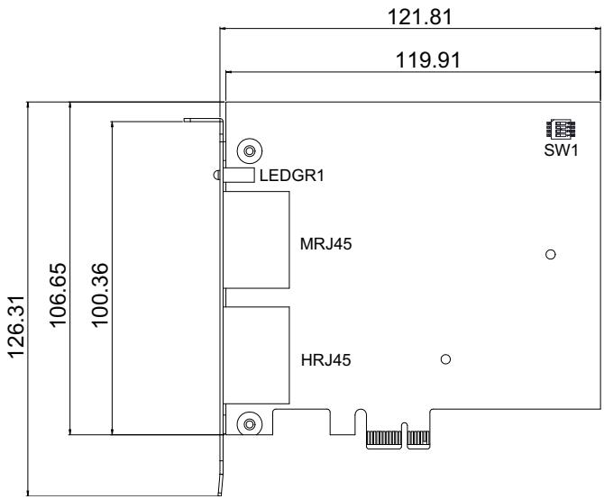
# 2.2 PCIe-7856 Mechanical Drawing

Dimensions: mm

![Pure technical line drawing of a mechanical component without any text, numbers, or symbols](.pcie-7856-53-50-15113-1010-11/a81f3bdbdb489b858c62742143a28a0eb87e3ef86887e2f3cc010a347ed6b3c1.jpg)

![MNET\nHSL](.pcie-7856-53-50-15113-1010-11/1644ffb3b6661547823c1ac0edea7e2194568e8fb59d44193fe2a9142cb5dc75.jpg)

![126.31\n106.65\n100.36\n121.81\n119.91\nLEDGR1\nMRJ45\nHRJ45\nSW1](.pcie-7856-53-50-15113-1010-11/7848a3a4d52eefc1e50601cac5dac51fa0aa6c50b15c8805bd5b9d81eaae53a2.jpg)

Figure 2-1: PCIe-7856 Mechanical Drawing

 MRJ45: MNET connection port
 HRJ45: HSL connection port
 SW1: Card identification switch
 LEDGR1: HSL/Motionnet Scan LEDs

# 2.3 Driver Installation

# 2.3.1 PCIe-7856

Open a web browser and navigate to the PCIe-7856/7853 product web page (https://www.adlinktech.com/Products/Motion\_Control/ DistributedMotionControl/PCIe-7856\_7853). Under Technical Resources, select Driver to see the list of available drivers. After downloading the required ZIP file, extract and double-click the enclosed executable file to run the installer. Follow the installation steps and, after installation is complete, restart the PC.

# 2.3.2 PCIe-7853

Open a web browser and navigate to the PCIe-7856/7853 product web page (https://www.adlinktech.com/Products/Motion\_Control/ DistributedMotionControl/PCIe-7856\_7853). Under Technical Resources, select Driver to see the list of available drivers. Download the HSL LinkMaster Utility for the PCIe-7853 and install it, following the onscreen instructions.

# 2.4 Troubleshooting

If the system doesn’t boot or if the PCIe board exhibits any erratic behavior, it is most likely caused by an interrupt conflict. After confirming the issue wasn’t caused by a simple oversight, the solution can be found by consulting the BIOS documentation that comes with your system. Check the Windows control panel on the connected PC to see if the card is listed by the system. If not, check the PCIe settings in the BIOS or use another PCIe slot.

# 2.5 Signal Connections

Signal connections of all I/O’s are described in the following two sub-sections. Please review this information before wiring any cables between the PCIe-7856 and slave modules.

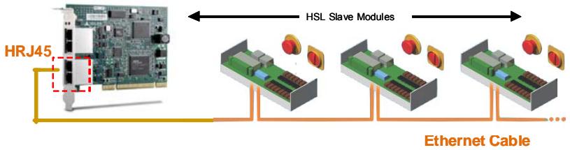
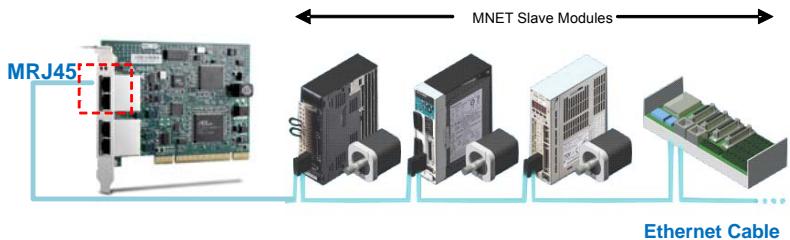
# 2.5.1 Connecting HSL/MNET Slave Modules

Wiring for MNET Motion Slave Modules
![MRJ45\nMNET Slave Modules\nEthernet Cable](.pcie-7856-53-50-15113-1010-11/0f1369361941f8144defd6970edc8071e42533e655c9cb35507976ae810ad5af.jpg)

Wiring for HSL I/O Slave Modules

![The diagram illustrates a connection topology between a central board and multiple peripheral modules.\n\n**Labeled Blocks:**\n*   **HRJ45:** Located on the left, this label points to a specific port on a circuit board, highlighted by a red dashed box.\n*   **HSL Slave Modules:** Located on the right, this label sits above three identical green modules arranged horizontally. Each module features red and yellow knobs.\n*   **Ethernet Cable:** Located at the bottom right, this label refers to the cabling connections.\n\n**Connections:**\n*   A yellow line originates from the **HRJ45** port and connects to the first green module.\n*   Orange lines connect the three **HSL Slave Modules** in a sequential daisy-chain fashion.\n*   The text **Ethernet Cable** indicates that these connections utilize Ethernet cabling.](.pcie-7856-53-50-15113-1010-11/863caeccc9eb69c0e5d6171f104b4a09503b79c0f0000875566fb60f91e40410.jpg)

Ethernet Cable (CAT5e Recommended)
![CAT5 CABLE\nCAT5 CABLE](.pcie-7856-53-50-15113-1010-11/a5b580b0d87774013f3066ba5aaa361446be1621f64d6becd3345f8f00072132.jpg)

# 2.5.2 RJ45 Pin Assignments

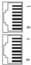
The Motionnet (MNET) master is the key component in charge of communicating with slave motion modules. The master sends commands to slave motion controllers and obtains motion status from them. The PCIe-7856 provides two MNET master connection ports for greater wiring flexibility. The pin assignments of the MRJ45 connector on the PCIe-7856 are as listed below:
![Two identical electrical connector pinout diagrams with no text or symbols](.pcie-7856-53-50-15113-1010-11/1ce7ef9de069f8c0f9faab05882932354ff1b6d2f35244edcd51a8556078a18d.jpg)

<table><tr><td>Pin No.</td><td>Pinout</td></tr><tr><td>1</td><td>NC</td></tr><tr><td>2</td><td>NC</td></tr><tr><td>3</td><td>NC</td></tr><tr><td>4</td><td>Data-</td></tr><tr><td>5</td><td>Data+</td></tr><tr><td>6</td><td>NC</td></tr><tr><td>7</td><td>NC</td></tr><tr><td>8</td><td>NC</td></tr></table>

The HSL master is the key component in charge of communicating with slave I/O modules. The master sends output values to, and gathers input information from, the slaves. PCIe-7856 provides two ports for HSL master connections for greater wiring flexibility. The pin assignments of the HRJ45 connector on the PCIe-7856 are as follows:

![Two identical electrical connector pinout diagrams with no text or symbols](.pcie-7856-53-50-15113-1010-11/2603ea424e473dee9630741fb9e8ba1a59daea8ef23532232ab9c5c898adb15a.jpg)

<table><tr><td>Pin No.</td><td>Pinout</td></tr><tr><td>1</td><td>NC</td></tr><tr><td>2</td><td>NC</td></tr><tr><td>3</td><td>RX+</td></tr><tr><td>4</td><td>TX-</td></tr><tr><td>5</td><td>TX+</td></tr><tr><td>6</td><td>RX-</td></tr><tr><td>7</td><td>NC</td></tr><tr><td>8</td><td>NC</td></tr></table>

# 2.5.3 HSL and Motionnet LED Indicators

The two LEDs on the PCIe-7856 provide communication status information. The red LED indicates MNET status and the green LED indicates HSL status. Before initialization of the PCIe-7856, both LEDs will be off. After initialization, the LEDs will begin blinking at a 1 Hz frequency.

When the PCIe-7856 connects to an HSL slave module, the green LED will turn on and remain constantly on during the scanning process, after which the green LED will continue blinking at 1 Hz.

When the PCIe-7856 connects to an MNET slave module, the red LED will turn on and remain constantly on until the scanning process stops or a communication error occurs, after which the red LED will continue blinking at 1 Hz.

![HSL Scan LED\nMotionnet Scan LED](.pcie-7856-53-50-15113-1010-11/8c7ee955fbe95244d8930ae66bd8bbc705f781f50c6c1cc0adbff6bd2c7534b7.jpg)

Figure 2-2: LED Indicators on the PCIe-7856

# 2.6 SW1 Card ID Switch Settings

The card ID can be set via the SW1 DIP switch as follows.

![SW1\nNC\nON\n1\n2\n3\n4\nNO\nON = 1\n0000 Card ID 0\n0001 Card ID 1\n0010 Card ID 2\n...\n...\n1110 Card ID 14\n1111 Card ID 15\nOFF = 0](.pcie-7856-53-50-15113-1010-11/a856344aa2c50d3f02975471137a2b81207d198aaff7f0b92e48e6d15ccbbea6.jpg)

This page intentionally left blank.

# 3 MNET Master-Slave Motion System

Motionnet (MNET) is an ultra-high-speed serial communication system proposed by Nippon Pulse Motor (NPM). It features strong performance with a maximum transfer speed of up to 20Mbps. The PCIe-7856 is equipped with one MNET port offering control of up to 256 axes via serial connections. ADLINK MNET solutions include not only single-axis controllers suitable for multiple PTP (point-to-point) movement applications, but also 4-axis motion controllers with support for linear and circular interpolation functions. Individual devices can control Panasonic A4 servo drivers. The controller can be used for executing continuous operations at constant speeds, performing linear as well as S-curve acceleration and deceleration, carrying out preset positioning operations, executing zero return operations, and so forth. As for connection distance, the cable length can be extended by up to 100 meters using an ordinary CAT5e LAN cable while connecting 64 axes at 20Mbps. All function library designs are compatible with ADLINK’s PCIe motion controllers and MNET bus motion controllers.

![**Labeled Blocks:**\n*   **PCle-7856**: An image of a green PCIe expansion card located at the top left.\n*   **Panasonic A4 Series**: An image of a grey industrial drive located in the center.\n*   **MNET-4XMO-(C) (4-axis Motion Controller)**: An image of a white terminal block module located at the bottom right.\n\n**Connections:**\n*   A thick blue line originates from the **PCle-7856** block.\n*   The line extends downward and connects to the text label: **Multi-drop Connection MNET Bus via CAT5/5e Cable**.\n*   From this central connection point, the line splits into two branches:\n    *   One branch connects upward to the **Panasonic A4 Series** block.\n    *   The other branch connects downward to the **MNET-4XMO-(C)** block.](.pcie-7856-53-50-15113-1010-11/3edb8b82b61b6abe996d34d469f701bb450d3ce4389ab8c5fb3c26d4eb5b6655.jpg)

Figure 3-1: MNET Distributed Motion Control System

# 3.1 MNET System Specifications

The two major functions of a Motionnet (MNET) system are serial communication and motion control.

<table><tr><td>Item</td><td>Specifications</td></tr><tr><td>Total serial communication line length (using recommended cables)</td><td>► Maximum of 100m (at a data transfer speed of 20 Mbps with 32 devices connected)► Maximum of 50m (at a data transfer speed of 20 Mbps with 64 devices connected)► Maximum of 100m (at a data transfer speed of 10 Mbps with 64 devices connected)</td></tr><tr><td>Serial communication interface</td><td>Pulse transformer and RS-485 specification line transceiver</td></tr><tr><td>Serial communication protocol</td><td>ADLINK proprietary protocol</td></tr><tr><td>Serial communication</td><td>NRZ signed</td></tr><tr><td>Serial communication method</td><td>Half-duplex communication</td></tr><tr><td>Connection method</td><td>Multi-drop connection using a LAN cable (CAT5/ CAT5e STP/S-STP)</td></tr><tr><td>Serial data transfer speed</td><td>20 Mbps/10 Mbps/5 Mbps/2.5 Mbps programmable speed setting</td></tr><tr><td>Maximum number of MNET modules</td><td>64 (the total number of axes will be 64 if all single-axis modules are connected or 256 if all modules belong to MNET-4XMO)</td></tr></table>

Table 3-1: MNET System Specifications

# 3.1.1 Wiring Cables

The PCIe-7856 system guarantees enhanced quality for highspeed communication and is designed to be connected with userprovided LAN cables suitable for 100BASE-T and 1000BASE-T. Because these cables have well-known specifications and are cheap and easy to obtain, we do not provide them and do not include them in our product lines. When selecting cables, make sure they meet one of the following standards.

# Wiring Standards

 TIA/EIA-568-B
 Category 5 (CAT5)
 Enhanced Category 5 (CAT5e)
 Category 6 (CAT6)

Choose UTP (Unshielded Twisted Pair) or STP (Shielded Twisted Pair) cables that meet one of the standards above. For an environment with excessive electromagnetic noise, use a shielded cable (STP).

Observe the following when connecting your system.

1. Keep the total serial line length as short as possible.
2. Maximum total serial line length will vary based on the data transfer speed and the number of local boards that are connected (this system employs a multi-drop connection method).
 20 Mbps with 32 modules connected: Max. 100 m
 20 Mbps with 64 modules connected: Max. 50 m
 10 Mbps with 64 modules connected: Max. 100 m

3. The shortest cable must be at least 60 cm long.
4. Do not mix cables of different types or models in the same serial line.
5. If using shielded cables, do not connect the shield on both ends to the FG terminals. Connecting only one end of the shield on each cable will improve noise immunity.

# 3.1.2 MNET System Communication

The following is a communication block diagram for a Missionnet (MNET) system.

![The flowchart displays a linear sequence of four blocks connected by red, double-headed arrows indicating bidirectional communication. The blocks and their labels are:\n\n1.  **Host** (Yellow block)\n2.  **Motionnet Bus** (Green block)\n3.  **MNET Single modules** (Blue block)\n4.  **Motion Amp.** (Pink block)\n\nThe connections are as follows:\n*   **Host** connects to **Motionnet Bus**.\n*   **Motionnet Bus** connects to **MNET Single modules**.\n*   **MNET Single modules** connects to **Motion Amp.**](.pcie-7856-53-50-15113-1010-11/d80cc8cc98cc0a63f5f0ee9d0dd0678908aa50303689444d9c8e4817a8596fbd.jpg)

<table><tr><td>Command Launching</td><td>Command Delivering</td><td>Command Dispatching</td><td>Command Executing</td></tr></table>

# Command Launching

Within the MNET system, remote modules communicate with each other using MNET network packets, but users do not need to understand the contents of these packets. Several API functions are provided for controlling modules and these functions are easy to understand and use.

API functions can analyze parameters from user commands and pack them as MNET network packets. The packets are then passed to remote modules. The remote modules will interpret the packets and execute the commands. Before launching a packet, all commands issued by the user are written into RAM and transferred on the MNET network.

RAM, therefore, is a bridge between the MNET master controller and the host PC. The RAM access time for one packet is about 600 ns and should be quite fast on the host PC. The delivery time for one command on the network will depend on the number of modules and the operating clock rate. In addition to using RAM, users can also write data into a FIFO queue in the central device and then issue a “send” command. This communication will be sent and received automatically by interrupting the cyclic communication. Complete command delivery time will depend on the number of MNET packets. One packet command can be delivered in one MNET scan (cycle) time.

# Command Delivery

For commands delivered as part of the cyclic communication process, the time allowed for communication by a single module is fixed. However, in a direct data communication the communication time will vary based on how the communication is controlled by the user’s program and the time needed to access the PCIe-7856.

![**Title:** Cyclic communication\n\n**Top Blocks & Connections:**\n- A bracket labeled **Send** encompasses two blue blocks: **Center** and **Local** connected by a red arrow pointing right.\n- A bracket labeled **Response** encompasses two blue blocks: **Local** and **Center** connected by a red arrow pointing right.\n- Text below the blocks reads: **Total of send and receive: 4 bytes**\n\n**Cylindrical Diagram (Ring):**\n- Lines connect the top blocks to specific points on the ring.\n- The ring is divided into sectors by vertical dashed lines.\n- Number **1** is near the left side.\n- Number **2** is above a right-pointing arrow on the top rim.\n- Number **3** is near the right side.\n- Number **4** is near the bottom right.\n- Number **5** is near the bottom left.\n- Text **64(max)** points to the sector at the bottom left.\n- An arrow inside the ring points left.\n- Text **ce image** is below the ring.\n\n**Bottom Section:**\n- Text **Interrupt** has an arrow pointing up to the ring.\n- A bracket connects **Interrupt** to the text **Data communication (Send, Receive)**.](.pcie-7856-53-50-15113-1010-11/dae696093210dba9a5ae9650a011101ebde02548b83a70481ab3a360cb004871.jpg)

Figure 3-2: MNET System Communication Sequence

# 3.2 MNET Motion Modules

Motionnet (MNET) motion slave modules are wire-saving solutions. ADLINK provides two types of general purpose 4-axis modules: MNET-4XMO and MNET-4XMO-C. Both offer crucial motion functions such as point-to-point, zero-position searching, programmable acceleration/deceleration, T/S curve speed profile, etc. In addition, the MNET-4XMO-C also supports high-speed position comparison, a trigger output function, and a point table for continuous contouring applications. For additional details, please refer to the MNET-4XMO Series User’s Manual available for download at: https://www.adlinktech.com/Products/Industrial\_Fieldbus/ Motionnet/MNET-4XMO-(C).

ADLINK has also provided single-axis motion modules with specific drivers for connecting to Panasonic A4 servos. These singleaxis modules have reached “end of life,” however, and the 4-axis modules are recommended as they can be conveniently plugged into any of those servos.

Regardless of the module and servo types involved, the servos themselves can be connected serially by the recommended cable type, greatly reducing wiring requirements.

<table><tr><td>Series</td><td>Model</td><td>Servo Driver</td><td>Axes</td><td>Mechanical I/O</td></tr><tr><td>MNET Single-axis Motion Modules</td><td>MNET-MIA</td><td>Panasonic A4</td><td>1</td><td>PEL, MEL, ORG, SD, EMG</td></tr><tr><td rowspan="2">MNET 4-axis Motion Modules</td><td>MNET-4XMO</td><td>General Purpose</td><td>4</td><td>PEL, MEL, ORG, SD, EMG</td></tr><tr><td>MNET-4XMO-C</td><td>General Purpose</td><td>4</td><td>PEL, MEL, ORG, SD, EMG, TRG</td></tr></table>

Table 3-2: MNET Motion Module Series

The MNET-MIA can control a servomotor when I/O signals from a Panasonic (Matsushita) servo amplifier MINAS A4 series (pulse command supporting type) servo amplifier CNI/F or CNX5 are routed directly to this connector: CN4.

These single-axis modules can control continuous operations of a servomotor with a variety of speed patterns (constant speed, linear acceleration/deceleration, S-curve acceleration/deceleration, preset positioning, and zero return) using serial communications.

Since these modules can connect directly to the mechanical I/O signals of a servo driver, they do not need the special servo driver cable required of conventional motion control modules, thus saving time and providing the following advantages: simplified wiring, shortened wiring runs, and reduction of problems caused by faulty wiring. They also offer high noise immunity, take full advantage of high-speed signal lines to handle command pulses, and are highly compact, especially since they conserve wiring space.

Again, ADLINK also offers general purpose 4-axis motion control modules which are highly recommended, especially if using servos or stepper motors that are not described above or if more advanced motion functionality is required (such as linear/circular interpolation). By using specific or general purpose D-Sub cables, these 4-axis modules can directly connect to servo drivers, including the Panasonic MINAS A4.

# 3.2.1 Motion Module Mechanical Drawings

![Pereonite\nM\nS\nM\nM\nM\nM\nM\nM\nM\nM\nM\nM\nM\nM\nM\nM\nM\nM\nM\nM\nM\nM\nM\nM\nM\nM\nM\nM\nM\nM\nM\nM\nM\nM\nM\nM\nM\nM\nM\nM\nM\nM\nM\nM\nM\nM\nM\nM\nM\nM\nM\nM\nN](.pcie-7856-53-50-15113-1010-11/d432c408fe1ca1fb37d875b0545a1ed48abb0b8f8f60b7d40a6dc92831731d3e.jpg)

![(62.6)\nSPEED\nT0\nA1\nADDRC 35\nA2\nSEL CH\nSWI](.pcie-7856-53-50-15113-1010-11/ddfed8a8662254b0e709bef7777d85c4883e35dd8ceb3e3129d96046e0936784.jpg)

units: mm

![52.4\n44\nCN1 CN2 CN1\n16.3](.pcie-7856-53-50-15113-1010-11/ab051c6de1468d6a7e4eb7ae5fb69612e4acde876dddbb6e557c88d86c46ff27.jpg)

![Pure mechanical assembly diagram without any text, numbers, or symbols](.pcie-7856-53-50-15113-1010-11/12614acbf80e04190bd10e7e71d77bfc10a57c7555e5079226d06c42b652c4fa.jpg)

![(3)\n64.3\n(2.2)](.pcie-7856-53-50-15113-1010-11/a540d1e05bd392d29ce0ffc3baae72e11f9dd7da6083430e25b9e00cb2267e54.jpg)

Figure 3-3: MNET-MIA with MINAS A4 Servo Driver

![74.9\n69\nCN1\nCM4\nCM3\nCM2\nCM1\nS3\nIOIF1\nIOIF2\nJP7\nJP3\nHS1\nHS2\nJP6\nJP5\nEMG\nJP4\nJ8\nS5\nIOIF3\nIOIF4\nON\nS2\nON\n1 2 3 4 5 6\n16 2.3\n16 5.3](.pcie-7856-53-50-15113-1010-11/050dfc705fbeb7da55829a4f62d828a65210f270e83419e2d6c1326285d3e0a0.jpg)

units: mm

Figure 3-4: MNET-4XMO-(C) Mechanical Diagram

This page intentionally left blank.

# 4 HSL Slave Modules

High Speed Link (HSL) is a master-slave network system featuring an innovative distributed architecture that modularizes communication, I/O functionality, and signal termination. ADLINK provides slave I/O modules and terminal bases to meet your particular application requirements, including discrete I/O, analog I/O, and motion control. For complete details about the modules, please refer to the HSL-4XMO User’s Manual, available here:

https://www.adlinktech.com/Products/Industrial\_Fieldbus/

HighSpeedLink(HSL)/HSL-4XMO

Slave I/O Modules: There are three groups of slave I/O modules with different dimensions. Slave I/O modules give terminal bases additional I/O capability. To identify each slave I/O module in a HSL network, a module type electronic data sheet is stored in the module itself. Slave I/O modules can also be located by address ID, set by a 6-bit DIP-switch. Depending on the I/O type, each slave I/O module may consume 1 or 2 address IDs. Since the greatest ID number in a HSL master is 63 (the highest value for a 6-bit unsigned integer), and since ‘0’ is reserved for the master, there are at most 63 slave I/O modules for each HSL master.

Terminal Bases: The function of a terminal base (TB) slave module is to facilitate convenient wiring. Both power and signal wiring go from the TB into the slave I/O modules. TBs can also facilitate RJ-45 connections between masters and slave I/O modules. With the help of a TB, slave I/O modules can be hot-swapped without interfering with other modules on the same HSL network.

U-series Modules: U-series slave modules provide direct I/O signal wiring on top of the device. They are more compact than TBs and offer several I/O interface types to facilitate signal linking.

HUB/Repeaters: HSL-HUB/Repeaters provide more sub-system flexibility and thus enable a greater variety of topologies.

Wiring Cables: The communication wiring cables between an HSL master and its I/O modules are standard 100 Base/TX with RJ-45 connectors, the same as commercial Ethernet cables.

# 4.1 HSL Slave I/O Modules

# 4.1.1 Discrete I/O Module

ADLINK provides a discrete M series daughter board form factor I/O module with aluminum cover.

<table><tr><td>Series</td><td>Model</td><td>Discrete Inputs</td><td>Discrete Outputs</td><td>Relay Outputs</td><td>Slave Index Occupation</td></tr><tr><td>M</td><td>HSL-DI32-M-N</td><td>32</td><td></td><td></td><td>2 (consecutive from odd number)</td></tr><tr><td></td><td>HSL-DO32-M-N</td><td></td><td>32</td><td></td><td>2 (consecutive from odd number)</td></tr><tr><td></td><td>HSL-DI16DO16-M-NN/PN</td><td>16</td><td>16</td><td></td><td>1</td></tr></table>

Table 4-1: HSL Discrete I/O Module Series

The selection guide is as follows:

![HSL - Discrete I/O Type - Series - Signal Type](.pcie-7856-53-50-15113-1010-11/8e1252620b9eb5633dc935376c7a05351d7ca79db7da828be527a66a5f8748b1.jpg)

 DI16DO16: 16 discrete inputs and 16 discrete outputs
 DI32: 32 discrete inputs
 DO32: 32 discrete outputs

 M: Daughter board with aluminum cover

 X: Input Signal Type: NPN sinking or PNP sourcing support

 Y: Output Signal Type: NPN sinking or PNP sourcing support

Table 4-2: HSL Discrete I/O Module Selection Guide

# 4.1.2 Analog I/O Modules

ADLINK provides M and U analog I/O modules, as shown below.

<table><tr><td>Series</td><td>Model</td><td>Analog Input</td><td>Analog Output</td><td>Slave Index Occupation</td></tr><tr><td>M</td><td>HSL-AI16AO2-M-VV</td><td>16</td><td>2</td><td>2 (leap number)</td></tr><tr><td>U</td><td>HSL-AO4</td><td></td><td>4</td><td>2</td></tr></table>

Table 4-3: HSL Analog I/O Module Series

The selection guide is as follows.

![The diagram is a block diagram illustrating a product code structure, organized into columns.\n\n**Top Row Blocks:**\n*   **HSL -**\n*   **Discrete I/O Type -**\n*   **Series -**\n*   **Signal Type**\n\n**Content Blocks (aligned vertically below the top row headers):**\n*   Below **Discrete I/O Type -**:\n    *   '► AI16AO2: 16 analog inputs and 2 analog out- puts'\n*   Below **Series -**:\n    *   '► M: Daughter board with aluminum cover'\n*   Below **Signal Type**:\n    *   '► X: Input signal type, V for voltage and A for current'\n    *   '► Y: Output signal type, V means voltage'](.pcie-7856-53-50-15113-1010-11/7dd3e8ed087db8b47b7fed732a2a52d8e948a9f787a0d7be589fc7e526c9221d.jpg)

Table 4-4: HSL Analog I/O Module Selection Guide

# 4.2 General Specifications

# 4.2.1 Digital I/O Modules

<table><tr><td rowspan="8">Discrete Input</td><td>Photo Couple Isolation</td><td colspan="2">2500 VRMS</td></tr><tr><td>Input Impedance</td><td colspan="2">4.7 kΩ</td></tr><tr><td>Input Voltage</td><td colspan="2">+24 V</td></tr><tr><td rowspan="2">Input Current</td><td>For NPN(1)</td><td>-10 mA</td></tr><tr><td>For PNP(2)</td><td>+10 mA</td></tr><tr><td rowspan="2">Operation Voltage (@ 24 VDC Power Supply)</td><td>For NPN(1)</td><td>ON: 11.4 VDC (max.)OFF: 14.3 VDC (min.)</td></tr><tr><td>For PNP(2)</td><td>ON: 12.6 VDC (min.)OFF: 9.8 VDC (max.)</td></tr><tr><td>Response Time</td><td colspan="2">ON: 8.8 μs (typical)OFF: 42 μs (typical)</td></tr><tr><td rowspan="4">Discrete Output</td><td rowspan="2">Switch Capacity</td><td>For NPN(3)</td><td>All channels: -50 mA/ch at 24 VDC</td></tr><tr><td>For PNP(4)</td><td>All channels: +50 mA/ch at 24 VDC</td></tr><tr><td rowspan="2">Response Time</td><td colspan="2">ON to OFF: 68 μs</td></tr><tr><td colspan="2">OFF to ON: 1.1 μs</td></tr><tr><td rowspan="5">Relay</td><td>Relay Type</td><td colspan="2">SPST, normally open, non-latching</td></tr><tr><td>Rating</td><td colspan="2">30 VDC/2 A, 250 VAC/2 A</td></tr><tr><td>Switching Frequency</td><td colspan="2">20 times/minute at rating load</td></tr><tr><td rowspan="2">Response Time</td><td colspan="2">ON to OFF: 3 μs (max.)</td></tr><tr><td colspan="2">OFF to ON: 6 μs (max.)</td></tr></table>

Table 4-5: Digital I/O Module

![This is an icon depicting a white document with a folded top-left corner and faint gray horizontal lines. A large, red checkmark is superimposed over the document.](.pcie-7856-53-50-15113-1010-11/aa70875c674b12b7b86d63ebf76e011523e90b690d6d2df89e3a630284328854.jpg)

(1) NPN sinking type sensor input modules.
(2) PNP sourcing type sensor input modules.
(3) NPN sinking type sensor output modules.
(4) PNP sourcing type sensor output modules.

# 4.2.2 Analog I/O Modules

<table><tr><td rowspan="5">Analog Input</td><td>A/D Resolution</td><td>16-bit (14-bit guaranteed)</td></tr><tr><td rowspan="2">Input Range</td><td>For VV type: ±10 V, ±5, ±2.5, ±1.25 V</td></tr><tr><td>For AV type: 20 mA, 10 mA, 5 mA</td></tr><tr><td>A/D Conversion</td><td>10 μs</td></tr><tr><td>Signal Type</td><td>16-ch Single Ended; 8-ch Differential</td></tr><tr><td rowspan="2">Analog Output</td><td>D/A Resolution</td><td>16-bit</td></tr><tr><td>D/A Settling Time</td><td>10 μs</td></tr></table>

Table 4-6: Analog I/O Modules

# 4.2.3 HSL Module DIP Switch

![DEV-0024411\nON\n1 2 3 4 5](.pcie-7856-53-50-15113-1010-11/952c284b9d6885e39a9236e114aa8e7c83647a3eaba9dcc66872c8a8bcc112e7.jpg)

Figure 4-1: HSL Module DIP Switch Location

![ON\n1 2 3 4 5 6](.pcie-7856-53-50-15113-1010-11/2516ebcf63b6800d7b08398eeac5eee99ecd52de88b04d0172590df4dad0d404.jpg)

$$
\mathrm{ON} = 1
$$

$$
1 0 0 0 0 0 \text {   address   } 1
$$

$$
0 1 0 0 0 0 \text {   address   } 2
$$

$$
\dots \dots
$$

$$
0 1 1 1 1 1 \text {   address   } 6 2
$$

$$
1 1 1 1 1 1 \text {   address   } 6 3
$$

$$
\mathrm{OFF} = 0
$$

![This image displays a white document icon featuring a folded top-left corner and horizontal lines representing text. A large red checkmark is superimposed over the right side of the document.](.pcie-7856-53-50-15113-1010-11/6c9db4ec5907032e880aec1c4796cb4261530652c6c7d938520e6d3b46cdc52b.jpg)
NOTE:

1. The address (or index) ‘0’ is reserved for the master.
2. HSL-DI32-M and HSL-DO32-M need two consecutive addresses starting from an odd number. For example, if the DIP switch is set to 3, it will occupy indexes 3 and 4.
3. HSL-AI16AO2-M-VV/AV needs two leap addresses in fullduplex mode. For example, if the DIP switch is set to 2, this module will occupy indexes 2 and 4.

# 4.2.4 Daughter Board/Module Dimensions

![100\n94\nØ3.2 4Ø7\n75\n78.2\n2.235\n46.43\n28\n82\n4\n92\n4.2\nk0](.pcie-7856-53-50-15113-1010-11/e27311020ba1adde80c5a1b76125405ff011a2e8be7f0dee6524b59b758a3775.jpg)

units: mm

M: Daughter board with aluminum cover (125 mm × 80 mm)
![100\n94\nØ3.2 4P1\n78.2\n2.235\n46.43\n28\n82\n9\n4\n92\n7.5\n4.2](.pcie-7856-53-50-15113-1010-11/dec97cd9a63e90475df83ac16175a234b060f59e341db5c1e06cdc61bbbf0aa8.jpg)

units: mm

U: Low-profile I/O module (71.8 mm × 138 mm)
![71.6\n53\n135\n138](.pcie-7856-53-50-15113-1010-11/7d4c44657ee96dd183503214c1f9bae51e5581311b0bc9d56fc44023105c15db.jpg)

![Technical line drawing of a mechanical assembly with mounting holes and internal components (no text or symbols)](.pcie-7856-53-50-15113-1010-11/d2353fb2df76b581363709616e082ea0912294d43325b74360de2d60a0a7e6b4.jpg)

units: mm

# 4.2.5 Wiring Diagrams

R (Relay Output):
![The image displays a block diagram enclosed within a large rectangular border. Inside the border, there are two primary blocks connected by two horizontal lines: a block on the left labeled **'Internal Circuit'** and a block on the right labeled **'SSR'**.\n\nAbove the **'Internal Circuit'** block, there is a diode symbol labeled **'LED'**.\n\nTo the right of the **'SSR'** block, two output terminals extend outward:\n*   The top terminal is labeled **'NO.n'**.\n*   The bottom terminal is labeled **'COM.n'**.\n\nOutside the main enclosure, a circuit connects to these terminals:\n*   A line from **'NO.n'** connects to a rectangle labeled **'Load'**.\n*   The right side of the **'Load'** rectangle connects to the positive terminal of a battery symbol.\n*   The negative terminal of the battery connects to the bottom wire, which originates from **'COM.n'**.\n*   To the far right, an AC source symbol (a circle with a sine wave) is present. A dashed line connects the bottom wire (from **'COM.n'**) to this AC source.](.pcie-7856-53-50-15113-1010-11/9ba4a2c84b8005ef9df5e15195b360f8fa059c60fcaf615c79a493ff87c4b3c4.jpg)

Analog Input (Differential Voltage Input):
![Based on the provided image, here is an accurate and concise description of the block diagram:\n\n**Labeled Blocks and Text:**\n*   **Differential Signal Source** (Top left label)\n*   **(30V** (Label next to the DC source symbol)\n*   **AGND** (Label next to the ground symbol)\n*   **IN(+)** (Label for the top input terminal)\n*   **IN(-)** (Label for the bottom input terminal)\n*   **ADC** (Label for the Analog-to-Digital Converter block)\n\n**Connections:**\n*   **Source to Inputs:** A top wire connects the upper terminal of the AC source (circle with sine wave) to the **IN(+)** terminal. A bottom wire connects the lower terminal of the AC source to the **IN(-)** terminal.\n*   **Source to Ground:** The lower terminal of the AC source is also connected to a DC source symbol labeled **(30V**, which connects to a ground symbol labeled **AGND**.\n*   **Inputs to ADC:** Inside a dashed enclosure, arrows point from the **IN(+)** and **IN(-)** terminals into the **ADC** block.](.pcie-7856-53-50-15113-1010-11/bc5905d6b0009d8675f6cb8aef853715add91beed00776c02cf8aba6718489d9.jpg)

Analog Input (Single-Ended Voltage Input):
![The diagram depicts a signal source connected to an Analog-to-Digital Converter (ADC).\n\n**Labeled Blocks:**\n*   **Source:** A circle containing a sine wave. To its left, the text 'Ground', 'Signal', and 'Source' is stacked vertically.\n*   **Input Terminals:** Inside a dotted rectangular boundary, there are two hexagonal terminals. The top one is labeled 'IN(+)' and the bottom one is labeled 'AGND'.\n*   **ADC:** A rounded rectangle labeled 'ADC'.\n*   **Ground Symbol:** A triangle pointing downwards connected to the source's bottom wire.\n\n**Connections:**\n*   A line connects the top output of the source circle to the 'IN(+)' hexagon.\n*   A line connects the bottom output of the source circle to the 'AGND' hexagon.\n*   The ground symbol connects to the bottom output line of the source circle.\n*   An arrow connects the 'IN(+)' hexagon to the 'ADC' block.\n*   An arrow connects the 'AGND' hexagon to the 'ADC' block.](.pcie-7856-53-50-15113-1010-11/b7d9a37d661ca26e425c6750480d684c0d36d7ad2a44d6e656fdb96ac96e144a.jpg)

# Analog Input (Current Measure):

![Based on the provided image, here is an accurate and concise description of the flowchart/block diagram:\n\n**Blocks:**\n*   **Current Source:** Labeled text above a circle containing an upward-pointing arrow.\n*   **Resistor:** Labeled **R** (zig-zag symbol). Below it, text reads **R=125 Ohm** and **%1 accuracy**.\n*   **Input Terminals:** Located inside a dashed box. The top terminal is labeled **IN(+)** and the bottom terminal is labeled **IN(-)**. Both have a hexagonal symbol next to them.\n*   **ADC:** A rectangular block on the right side labeled **ADC**.\n\n**Connections:**\n*   The **Current Source** and resistor **R** are connected in parallel.\n*   Two arrows point from the top and bottom rails of the parallel circuit into the input section inside the dashed box.\n*   Inside the dashed box, arrows connect the input terminals to the **ADC** block:\n    *   An arrow connects **IN(+)** to the top input of the **ADC**.\n    *   An arrow connects **IN(-)** to the bottom input of the **ADC**.](.pcie-7856-53-50-15113-1010-11/a94cf8916ece0b486b4727acf2b4c2a81297acc9d34879812c510f3a345d62ab.jpg)

# N (NPN Sinking-type Sensor Input):

![Circuit\nV+\n4.7kΩ\nIN\nG\nLED\nInternal Circuits](.pcie-7856-53-50-15113-1010-11/135ec8df74c510f3afb60874084e8af78a9afa01a710430ae22574366e8f14b4.jpg)

# N (Dry Contact Input):

![V+\n4.7kΩ\nIN\nI\nG\nLED\nInternal Circuits](.pcie-7856-53-50-15113-1010-11/a968d7179d39ed6d16576ee3ce968be7c1953c817cdbeb18d1ea002e7d3473d1.jpg)

P (PNP Sourcing-type Sensor Input):
![Circuit\nV+\nIN\nG\n4.7kΩ\nLED\nInternal Circuits](.pcie-7856-53-50-15113-1010-11/5fd2007cfb5260e1a510c5bb92797b2d7ed00a796a714d61337278910bb01cfb.jpg)

P (Wet Contact Input):
![V+\nIN\n4.7kΩ\nG\nLED\nInternal Circuits](.pcie-7856-53-50-15113-1010-11/a94a2a8e6b0d3afc351748d3428641c8e8a77e00c1787e4e9f97df321c2b7fc8.jpg)

N (NPN Sinking Output):
![LED\nInternal\nCircuits\nV+\nLoad\nOut\nG](.pcie-7856-53-50-15113-1010-11/6f50fe5b1af07dedd8fb19721a7933f103e292baf9b9d8af5598e2484bc1c545.jpg)

P (PNP Sourcing Output):
![LED\nInternal Circuits\nV+\nOut\nLoad\nG](.pcie-7856-53-50-15113-1010-11/7c426a20470ad2f0cea67b71330a449f5e39c6db9004a35a8d50883633957e7d.jpg)

# 4.2.6 Terminal Base Motion Control Modules

The terminal bases (TBs) include:

 HSL-TB32-U-DIN
 HSL-TB64-DIN
 HSL-TB32-M-DIN
 HSL-TB32-MD

# Features

 Field I/O wiring connection for HSL I/O modules
 Screw or spring terminal for easy field wiring
 Power and ground included for each signal channel
 Interlocking design for rugged installation
 Power LED indicator
 DIN rail mount
 Onboard terminator resistor

General Descriptions

<table><tr><td>Series</td><td>Model</td><td>Description</td><td>Module Support</td></tr><tr><td rowspan="2">DB</td><td>HSL-TB32-U</td><td>(1) 32-channel direct connection terminal base(2) One DB slot</td><td>All HSL DB-series modules</td></tr><tr><td>HSL-TB64</td><td>(1) 64-channel direct connection terminal base(2) Two DB slots</td><td>All HSL DB-series modules</td></tr><tr><td rowspan="2">M</td><td>HSL-TB32-M</td><td rowspan="2">32-channel direct connection terminal base for HSL M-series modules</td><td rowspan="2">All HSL M-series modules</td></tr><tr><td>HSL-TB32-MD</td></tr></table>

# Jumper Settings

Since HSL is a serial transmission system, a terminator should be set at the end of the cable. Each TB has a jumper-selectable terminator on board. Only the last module needs to have the terminator enabled.

Not the last module (Default)
![5 3 1\nOFF ON\n6 4 2](.pcie-7856-53-50-15113-1010-11/4c056d370419599ab59ea71c9684e26d232ad1ecd53acc65606b733abd93c2f9.jpg)

The last module
![5 3 1\nOFF ON\n6 4 2](.pcie-7856-53-50-15113-1010-11/ac1729798d6412aed1d0caf20564b48e13fecc7e5f921c7bfccd9f4a6197c278.jpg)

# HSL-TB32-MD Jumper Settings

JP1,2 (External Power Option)
![1 2 3\n1 2 3](.pcie-7856-53-50-15113-1010-11/cb8a192031f89168cc54fcffd95f3b0b4b74f178fe9b12e3abaf5f8091671290.jpg)

1,2 short: Different Power (Default)
2,3 short:Common Power

JP3 (Tx Terminal Resistor)
![ON\n3\n2\n1\nOFF\nOFF is default setting](.pcie-7856-53-50-15113-1010-11/6812881ec86d4d155160cca1a2706e156c0abf64da34c6b5ff3812bc2a734cc5.jpg)

JP4 (Rx Terminal Resistor)
![ON\n3\n2\n1\nOFF\nOFF is default setting](.pcie-7856-53-50-15113-1010-11/2828bd9d800c5693a3ad1cc17de63bc4b137b675782497651ef34ad3e88adb4e.jpg)

JP5 (Fuse Option)
![1\n2\n3\nON\nOFF](.pcie-7856-53-50-15113-1010-11/8558ba420c4ce20b885c5daa42834590601fcd9353b83d14d039fe7e3d031fc0.jpg)

1,2 short: With Fuse
2,3 short:Without Fuse (Default)

# Dimensions

DB with HSL-TB32-U-DIN (126 × 120.1 × 107.3) mm

![126\n120.1](.pcie-7856-53-50-15113-1010-11/4657323f761b607a0527f4eba92edc7e2027bc26954b76624d6db027dc988419.jpg)

units: mm

![Pure technical line drawing of a mechanical assembly without any text, numbers, or symbols](.pcie-7856-53-50-15113-1010-11/b94a5503f5d4bc7e6cd886621d24ac0aba9bdfac08533e7771a4c418f6751e7d.jpg)

![10.4\n10.3](.pcie-7856-53-50-15113-1010-11/cc5ce7a58ec5cf2d4c4a44c15f49e8a713fd7848b0d233e69c5fc301b70bf158.jpg)

![168.7\n120.7](.pcie-7856-53-50-15113-1010-11/a2e558bc7bc62a01cc19483c7a7120d9ce5b6f5c1d71bf985143e3a31248a695.jpg)

![Technical line drawing of a mechanical assembly with spring-loaded components and a 720mm dimension label (no text or symbols beyond measurement)](.pcie-7856-53-50-15113-1010-11/42ef8410a47af648af0f9194e4d24de1a0bb8653726a0e7d5418a8dea4690150.jpg)

![63\n0.5](.pcie-7856-53-50-15113-1010-11/8688db764ea99fd416ce833e6db43ab5a57934d757f89d9c2d9cf2b76a0b1e22.jpg)

DB with HSL-TB64-DIN (168.7 × 120.1 × 107.3) mm
![168.7\n120.7](.pcie-7856-53-50-15113-1010-11/a1fbf6109c3d5587c409a601250c803217e306bd957eafad615a3b8eb8ab0b41.jpg)

units: mm

![Technical line drawing of a mechanical assembly with spring and base components (no text or symbols)](.pcie-7856-53-50-15113-1010-11/e491c3b1d5830985ded76e56abd7f81efee135cb771f04b14b60106a5dd92f0c.jpg)

![6.3\n8.3](.pcie-7856-53-50-15113-1010-11/350f226989215b47badc8266d6fdd899602538cf800484f8f5c95c744f8f622c.jpg)

M module with HSL-TB32-M-DIN (128.5 × 85.5 × 108) mm
![128.5\n85.6](.pcie-7856-53-50-15113-1010-11/b0e012efddfdb45895bb5c7482449d35f6f8a717a3edd27d50c6bc36d3373d86.jpg)

units: mm

![Pure architectural line drawing of a building facade with no text, numbers, or symbols](.pcie-7856-53-50-15113-1010-11/d0b1d4e79c31b10ae870fe1385fb4405724c04701adb6d42248c9d337284ee02.jpg)

![4.5,7\n108](.pcie-7856-53-50-15113-1010-11/369ff1b6dc094ebfe054ca07a296209783d2cac82811d83f0ec7f087e9bc0cb3.jpg)

HSL-TB32-MD (129 × 107) mm

units: mm

![107\n129](.pcie-7856-53-50-15113-1010-11/30b2728afd1bd5b7b7617f391e134e0774c75ce5679310288792f4dce856babe.jpg)

# 4.2.7 Managing Slave Indexes in an HSL Network

# Before Proceeding

Before powering on the slave modules, ensure the DIP switch is properly set. Refer to Section 4.2.3 on page 28 and take special note of the following:

1. One master controller can connect to a maximum of 63 slave modules.
2. The more compact the slave addresses, the more efficiently the HSL system can work.
3. Discrete I/O and relay module rules:

<table><tr><td>Module</td><td>Slave Index Occupation</td><td>Transmission Mode</td><td>Transmission Speed</td></tr><tr><td>HSL-DI16DO16-M-NN/PN</td><td>1 (any address)</td><td rowspan="3">Full-duplex (fixed)</td><td rowspan="3">6 Mbps (fixed)</td></tr><tr><td>HSL-DI32-M-N/P</td><td rowspan="2">2 (consecutive from odd number)</td></tr><tr><td>HSL-DO32-M-N/P</td></tr></table>

4. Analog I/O and thermocoupling module rules:

<table><tr><td>Module</td><td>Slave Index Occupation</td><td>Transmission Mode</td><td>Transmission Speed</td></tr><tr><td>HSL-AI16AO2-M-VV</td><td rowspan="2">2 (leap number)</td><td rowspan="2">Full-duplex (fixed)</td><td rowspan="2">3/6/12 Mbps (selectable)</td></tr><tr><td>HSL-AO4-U</td></tr></table>

5. Special rule: If installing only one HSL-AI16AO2-M-VV and the DIP switch is set to 1 (the HSL-AI16AO2-M-VV only supports full-duplex mode), the occupied indexes will be 1 and 3. You must assign a value of 4 to the parameter “MOD\_No” of “APS\_set\_field\_bus\_slave\_param()” to ensure correct communication (PCIe-7856 only).

# Examples

The following examples are provided for user reference. All the modules involved are assumed to be in full-duplex mode.

# Example 1

HSL-DI16DO16-UD×2, HSL-DI32-MN×2, and HSL-AI16AO2- VV×1 are installed (with all slave modules in full-duplex mode) under two different conditions:

Condition 1: HSL-AI16AO2-VV operating at 6 Mbps.

ADLINK suggests the following slave index configuration:

<table><tr><td>Item</td><td>DIP Switch</td><td>Index Occupation in HSL</td></tr><tr><td>HSL-DI32-M-N #1</td><td>1</td><td>1, 2</td></tr><tr><td>HSL-DI32-M-N #2</td><td>3</td><td>3, 4</td></tr><tr><td>HSL-AI16AO2-VV</td><td>5</td><td>5, 7</td></tr><tr><td>HSL-DI16DO16-UD #1</td><td>6</td><td>6</td></tr><tr><td>HSL-DI16DO16-UD #2</td><td>8</td><td>8</td></tr></table>

This is an example of a compact composition. The scan time will be 30.33 µs × 8 at 6 Mbps, full-duplex mode. Users can connect the modules with one master controller.

Condition 2: HSL-AI16AO2-VV×1 operating at 12 Mbps.

ADLINK recommends the following slave index configuration.

<table><tr><td>Item</td><td>DIP Switch</td><td>Index Occupation in HSL</td></tr><tr><td>HSL-DI32-M-N #1</td><td>1</td><td>1, 2</td></tr><tr><td>HSL-DI32-M-N #2</td><td>3</td><td>3, 4</td></tr><tr><td>HSL-DI16DO16-UD #1</td><td>5</td><td>5</td></tr><tr><td>HSL-DI16DO16-UD #2</td><td>6</td><td>6</td></tr></table>

This is another example of a compact composition. The scan time required is 30.33 µs × 6 at 6 Mbps, full-duplex mode. Users may connect these modules with one master controller.

The HSL-AI16AO2-M-VV module will connect to another master controller. The DIP switch of HSL-AI6AO2-M-VV will be assigned a value of 1.

![HSL-D16DO2-UL ×2, HSL-DI32-UD × 2\nHSL-AI16AO2-M-VV\n6 Mbps\n12 Mbps](.pcie-7856-53-50-15113-1010-11/c762b820ff510f38d9bd741b6a55d5877012c9bf2a5d6b5332a491c297962cdb.jpg)

Consequently, the cycle time of the first master controller is 30.33 µs × 6 and the cycle time of the second master controller is 45.5 µs at 12 Mbps, full-duplex mode.

# Example 2

Two HSL-DI16DO16-UJ’s, one HSLDI16DO16-M-NN, two HSL-DO32-M-N’s and one HSL-AI16AO2-VV are installed (with all slave modules in full-duplex mode) under two different conditions:

Condition 1: HSL-AI16AO2-VV module operating at 6 Mbps.

ADLINK recommends the following slave index configuration:

<table><tr><td>Item</td><td>DIP Switch</td><td>Index Occupation in HSL</td></tr><tr><td>HSL-DO32-M-N #1</td><td>1</td><td>1, 2</td></tr><tr><td>HSL-DO32-M-N #2</td><td>3</td><td>3, 4</td></tr><tr><td>HSL-AI16AO2M-VV</td><td>5</td><td>5, 6</td></tr><tr><td>HSL-DI16DO16-UJ #1</td><td>7</td><td>7</td></tr><tr><td>HSL-DI16DO16-UJ #2</td><td>8</td><td>8</td></tr><tr><td>HSL-DI16DO16-M-NN</td><td>9</td><td>9</td></tr></table>

The scan time will be 30.33 µ ×17 at 6 Mbps, full-duplex mode. These modules can be connected with one master controller.

Condition 2: HSL-AI16AO2-VV module operating at 12 Mbps.

ADLINK recommends the following slave index configuration:

<table><tr><td>Group 1</td><td>DIP Switch</td><td>Index Occupation in HSL</td></tr><tr><td>HSL-DO32-M-N #1</td><td>1</td><td>1, 2</td></tr><tr><td>HSL-DO32-M-N #2</td><td>3</td><td>3, 4</td></tr><tr><td>HSL-DI16-UJ #1</td><td>5</td><td>5</td></tr><tr><td>HSL-DI16-UJ #2</td><td>6</td><td>6</td></tr><tr><td>HSL-DI16DO16-M-NN</td><td>7</td><td>7</td></tr></table>

The scan time required is 30.33 µs × 7. These modules may be connected with one master controller. The HSL-AI16AO2-M-VV module will connect to another master controller. The management table and illustration below are provided for reference.

<table><tr><td>Group 2</td><td>DIP Switch</td><td>Index Occupation in HSL</td></tr><tr><td>HSL-AI16AO2-M-VV</td><td>1</td><td>1, 2</td></tr></table>

<table><tr><td>Group 1</td></tr><tr><td>Group 2</td></tr></table>

![6 Mbps\n12 Mbps](.pcie-7856-53-50-15113-1010-11/c72865ac7db13a09b9342e2c8eae0624db3d0221d2b8be48ea7872e971e18385.jpg)

![Green printed circuit board with various electronic components and connectors (no readable text or symbols)](.pcie-7856-53-50-15113-1010-11/8fb3970fb4196ce57395f22c9a15a12b4f6a03827c6cac51567c177fa84cc680.jpg)

The cycle time of the first master controller will be 30.33 µs × 7 while the cycle time of the second master controller will be 15.17 µs × 11 at 12 Mbps, full-duplex mode.

# 5 MotionCreatorPro 2 (MCP2)

After installing the hardware, it is necessary to correctly configure all cards and double-check the system before running. This chapter provides guidelines for establishing a control system and manually testing the PCIe-7856 to verify correct operation. The MCP2 software provides a simple yet powerful means to set up, configure, test, and debug a motion control system that uses PCIe-7856.

# 5.1 About MCP2

Before running MCP2, please note the following.

1. MCP2 was developed using BCB 6.0 and is available only for Windows systems with a screen resolution of 1024x768 or higher. It cannot be run under DOS.
2. The following files are required by the program:

 MCP2.mdb, which stores parameters and graphics.

 MCPro2.ini, which stores initialization settings.

3. MCP2 is a highly integrated program that supports many ADLINK motion control cards. Multiple cards can be used in one system.

# 5.2 How to Run MCP2

After installing the software drivers for PCIe-7856, the MCP2 program will be located at “&lt;chosen path&gt;\MCP2.exe”. Double click the executable file to run the program.

# 5.3 MCP2 Features

# 5.3.1 Main Menu

Launching MCP2.exe will present the user with the main menu. Refer to the following images and descriptions for details on all the available features. To exit the program at any time, select “Exit” from the “File” menu.

![MotionCreatorPro2\nFile View Initial Options Function About\nMisc. Function\nADLINK\nPCIe-7856\nCard No 0\nHSL BusNo 0\n(ID1) HSL-DI32\n(ID62) HSL-DO32\nMNET BusNo 1\n(ID0) MNET-4XMO\nAxisNo = 1500 ServoOff\nAxisNo = 1501 ServoOff\nAxisNo = 1502 ServoOff\nAxisNo = 1503 ServoOff\n(ID63) MNET-4XMO-C\nAxisNo = 1504 ServoOff\nAxisNo = 1505 ServoOff\nAxisNo = 1506 ServoOff\nAxisNo = 1507 ServoOff\nVersion Info\nADLINK\nTECHNOLOGY INC.\nBoard ID: 0\nAPS Library: 191004\nDriver: 1606161\nADCNC Library: 2014111701\nCPLD/FPGA: 20190917\nCarrier Board: 0\nB\nC](.pcie-7856-53-50-15113-1010-11/4e74a2cde0b0ca06b2322e02998ec4be375c693a7ad662506010dba4f9ffbdf0.jpg)

A. Icons for operation modes. Some will be active when a bus/motion item in the tree view is selected and some will be active when an axis item is selected.

 Function Buttons

 Configuration

<table><tr><td>Button</td><td>Function</td><td>Description</td></tr><tr><td>&lt;img src="images/46fbcb3315a1c46cf6d78d71f8af2c93ff6faeaa72cd4e0d30f7cbf15e145a81.jpg"/&gt;</td><td>Axis/Board Configuration</td><td>Set axis/board parameters.</td></tr></table>

#  Movement

<table><tr><td>Button</td><td>Function</td><td>Description</td></tr><tr><td>&lt;img src="images/88504e17baa0046c736fed90de1eb78e4bf71e295c7c112547797585595fe6fe.jpg"/&gt;</td><td>Single Movement</td><td>Single-axis movement (PTP), including absolute and relative functions.</td></tr><tr><td>&lt;img src="images/01580bce5b959ee46dfa7afae9918086cf55fe8e8e607c83ece2abe5fb35ffa4.jpg"/&gt;</td><td>Home Return Movement</td><td>Home return movement.</td></tr><tr><td>&lt;img src="images/ee5bebf14d69375b967ea6722baaa12f0e30b6cb771ddfcce806d2169b49abcd.jpg"/&gt;</td><td>Interpolation</td><td>Interpolation function.</td></tr><tr><td>&lt;img src="images/16e96e98caac4855d1806875e86acdba850c57dc7710fd4ff22ba915aab9b89f.jpg"/&gt;</td><td>Sampling</td><td>Sampling function. Select this to set the source and draw its profile.</td></tr><tr><td>&lt;img src="images/ac4588000c8749f5fa4e93e9d3599b443bf3bff44d552a1a140c2eed1f776b9d.jpg"/&gt;</td><td>2D Movement</td><td>Execute 2D motion.</td></tr></table>

#  Field Bus

<table><tr><td>Button</td><td>Function</td><td>Description</td></tr><tr><td>&lt;img src="images/bb26b06300b921be6abf469f7cdb7967945937c2147fb48d89fe17cf7055fdc0.jpg"/&gt;</td><td>Field Bus Connect</td><td>Connect an MNET/HSL module. Select baud rate (to the right of the button) and connect.</td></tr><tr><td>&lt;img src="images/0136d11fa49f75a6e7db3fbcb0e0a9f1bd7d6e02acbd01744761b3d3665d1f6e.jpg"/&gt;</td><td>Field Bus Disconnect</td><td>Disconnect an MNET/HSL module.</td></tr><tr><td>&lt;img src="images/46b3a82744caf1257aa071d862db1bc2aa7f54845758ae2dafe1cf4c7c6d512c.jpg"/&gt;</td><td>Field Bus Module Test</td><td>If properly connected, a module can be selected here for a module test.</td></tr></table>

B. All automation products found by MCP2. The tree view will display motion axes as well as field bus I/O.

<table><tr><td>ICON</td><td>Function</td><td>Description</td></tr><tr><td>(Yellow)</td><td>Warning</td><td>Servo warning.</td></tr><tr><td>(Red)</td><td>Alarm</td><td>Servo alarm.</td></tr><tr><td>(Black)</td><td>Normal (Servo OFF)</td><td>No error and servo is off.</td></tr><tr><td>(Green)</td><td>Normal (Servo ON)</td><td>No error and servo is on.</td></tr></table>

C. Board information, including software, firmware, and hardware version numbers.

# 5.3.2 HSL Distributed I/O Manager

This page can be used to test the HSL system and slave modules. After executing the I/O management page, the main operation window shown below will appear. You can select the module for testing in the tree list of left window. The corresponding ID will also appear with each module. For example, the following figure shows the management pane for the HSL-AI16AO2-VV module. Analog input information is presented in this window and you can use the sliding bar to control the analog output.

![AITEAD2_VV PCI 3000 Module ID - 5\nA)\nB\nC\nD\nA\nAITEAD2_VV PCI 3000 Module ID - 5\nA1\n0\n88.816\n88.884\n88.189\n88.716\n88.748\n88.799\n88.383\n88.464\n8\n88.530\n88.587\n88.651\n88.642\n88.641\n88.631\n88.633\n87.944\nA0\n0\n1\n40\n10\n-10\n10\nStore Status Quality\nFINE\nBAD\nDISCONNECT](.pcie-7856-53-50-15113-1010-11/64e4cadb061048102fe2268c23fb7139ea9b751ef61c41e9191f1a6bd23da1b0.jpg)

# Operation Instructions

A. Tree view of all HSL and MNET modules.
B. Analog input presentation.
C. Analog output control panel.
D. Check the communication status of each module.

![MotionCreatorPro2\nFile View Initial Options About\nField Disconnect Field Module\nADLINK PCIe-7856\nCard No 0\nHSL BusNo 0\n(ID1) HSL-DI32\n(ID62) HSL-DO32\nMNET BusNo 1\n(ID0) MNET-4XMO\nAxisNo = 1500 ServoOff\nAxisNo = 1501 ServoOff\nAxisNo = 1502 ServoOff\nAxisNo = 1503 ServoOff\n(ID63) MNET-4XMO-C\nAxisNo = 1504 ServoOff\nAxisNo = 1505 ServoOff\nAxisNo = 1506 ServoOff\nAxisNo = 1507 ServoOff\nDI32 PCIe-7856 Module ID = 1\nDI\n15 14 13 12 11 10 9 8 7 6 5 4 3 2 1 0\n31 30 29 28 27 26 25 24 23 22 21 20 19 18 17 16\nSlave Status Quality BAD FINE\nDI-Interrupt\n15 14 13 12 11 10 9 8 7 6 5 4 3 2 1 0\n31 30 29 28 27 26 25 24 23 22 21 20 19 18 17 16\nDO32 PCIe-7856 Module ID = 62\nDO\n15 14 13 12 11 10 9 8 7 6 5 4 3 2 1 0\n31 30 29 28 27 26 25 24 23 22 21 20 19 18 17 16\nSlave Status Quality BAD FINE\nA B C D](.pcie-7856-53-50-15113-1010-11/5cd62095cec925980f14eaaba6c1840adb5e1819bb275ae6160eae7cec54ad70.jpg)

# Operation Instructions

A. Tree view of all HSL and MNET modules.
B. Digital input representation or digital output control.
C. Check the communication status of each module.

# 5.3.3 MNET Distributed Motion Manager

The Motionnet (MNET) manager offers several motion operations, including single-axis movement, home return, axis parameter setting, etc.

Parameter Management
![MotionCreatorPro2\nFile View Initial Options Function About\nAxis/Board Plans Single Move Home Move Fast Disconnect Field Mode\nADLINK PCle-7856 Card No 0\nAxis Parameter MNET PCIe-7856 CardNo =0\nAxis Configuration Axis Select\nAxisNo1500 AxisNo1501 AxisNo1502 AxisNo1503\nEL_LOGIC Not Inverse Not Inverse Not Inverse Not Inverse\nORG_LOGIC Active Low Active Low Active Low Active Low\nEL_MODE Dec Stop Dec Stop Dec Stop Dec Stop\nMDN_CONDI Cmd Done Cmd Done Cmd Done Cmd Done\nALM_LOGIC Active Low Active Low Active Low Active Low\nEZ_LOGIC Active Low Active Low Active Low Active Low\nSPEL_EN Disable Disable Disable Disable\nSMEL_EN Disable Disable Disable Disable\nEFB_POS0 100000 100000 100000 100000\nEFB_POS1 -100000 -100000 -100000 -100000\nHOME_MODE Mode 0 Mode 0 Mode 0 Mode 0\nHOME_DIR Positive Dir. Positive Dir. Positive Dir. Positive Dir.\nHOME_VM 10000 10000 10000 10000\nHOME_EZA 0 0 0 0 0\nHOME_VO 152 152 152 152\nHOME_OFFSET 100 100 100 100\nCURVE T-Curve T-Curve T-Curve T-Curve\nACC 1999E7 1999E7 1999E7 1999E7\nSet To Card Save To Flash Save To File Load Default\nLoad From Card Load From Flash Load From File](.pcie-7856-53-50-15113-1010-11/70f1f3334ee43322d2ea25ee14fff7235988ccb4a34571f1f423db8d73305c9f.jpg)

# Operation Instructions

A. Tree view of all HSL and MNET modules.
B. Parameter values of each axis.
C. Parameter management buttons for saving/loading parameters in various ways. “Set To Card” must be clicked to activate any changes made to this table.

Tip: Right-click on a parameter to apply it to all other axes.

Single-axis Movement
![PCIe-7856 MNET ID = 0 AxisNo 1500\nCommand : 0\nPosition : 0\nCmd Vel : 0\nFBK Vel : 0\nErr Pos : 0\nTargetPos : 0\nSet Pos : 0\nMaxVel : 0\nABS MOVE\nPosition 1 Position 2\nForward Backward\n0 0\n0 0\nREL MOVE\nForward Backward\n0 0\nSpeed Profile Preview\nPreview\nInterrupt List\nINSTP EPSL\nIACCS ENSL\nIACCE EGCM\nIDECS EPEL\nIDECE EMEL\nISPEL EALM\nISMEL EEMG\nICOMP ESD\nICLRC EPES\nIORGC ESIP\nISD EPBO\nEPCO EEAB\nEPAB EPAB\nEMG STOP R Mode STOP\nDelayTime: 1000\nCIP LIP SMV HMV NSTP DEC ACC VM CSTP\nSMELS SPELS MELS PELS ALMS EMGS ASTP VS\nRDY SVON INP EZ EMG ORG MEL PEL ALM\nEPAB EEAB EPCO EPBO ESIP EPES ESD EEMG EALM EMEL EPEL EGCM ENSL EPSL\nISD IORGC ICLRC ICOMP ISMEL ISPEL IDECE IDECS IACCE IACCS INSTP](.pcie-7856-53-50-15113-1010-11/5af761bbec1c5c8873c695431874aedfb7589aff5431ed565f124b57ce0e9802.jpg)

# Operation Instructions:

A. Command, feedback, error, and target position information. Command and feedback speed information. The minimum speed value may be limited by speed calculation cycle time for low speed display.
B. Optional operation settings and buttons. Repeat Mode can be used in both Relative and Absolute mode. The axes will move between two positions or forward/backward distance cyclically. You can set the delay time (in milliseconds) between each move. The minimum value is 1 ms. The stop button is for relative, absolute, and velocity modes.

C. Operation buttons and settings for 3 modes. You can switch operation between relative, absolute, and velocity modes. Before operation, mode parameters must be set, such as positions 1 and 2, forward/backward distance, and forward/backward velocity. Set “MaxVel” before executing relative or absolute mode. While using jog mode, the other three modes will be disabled.

D. Motion status, I/O status, and interrupt status display area.

Home Return
![PCIe-7856 MNET ID = 0 AxisNo 1500\nHome EZA : 0\nHome Offset : 100\nHome VM : 10000\nHome VO : 152\nSelect Mode : 0\nHome Direction : Positive\nB\nCommand : 0\nC\nFeedback : 0\nStart Stop Set Param To Card Load Param From Card\nCIP LIP SMV HMV NSTP DEC ACC VM CSTP\nE SMELS SPELS MELS PELS ALMS EMGS ASTP VS\nRDY SVON INP EZ EMG ORG MEL PEL ALM\nHome_Search Mode = 0 ORG → Down → Stop\nF\nORG SD EL\nCase 1 (SD-inactive) Reset\nCase 2 (SD-inactive) Reset\nCase 3 (SD-inactive) Reset\nCase 1 (SD-active) Reset\nCase 2 (SD-active) Reset\nCase 3 (SD-active) Reset\nORG Offset ORG Offset ORG Offset ORG Offset ORG Offset ORG Offset ORG Offset ORG Offset ORG Offset ORG Offset ORG Offset ORG Offset ORG Offset ORG Offset ORG Offset ORG Offset ORG Offset ORG Offset ORG Offset ORG Offset ORG Offset ORG Offset ORG Offset ORG Offset ORG Offset ORG Offset ORG Offset ORG Offset ORG Offset ORG Offset ORG Offset ORG Offset ORG Offset ORG Offset ORC\n: Start Point VS: Start Velocity VM:Max Velocity](.pcie-7856-53-50-15113-1010-11/1ec2da0bb850185f745bfe1ab1ca3c4949a1ca0227c4ab5410acdea423baf3d3.jpg)

# Operation Instructions

A. Speed parameter of the homing profile. Refer to area F.
B. Mode setting for the homing function, selectable via pulldown menu.
C. Command and position information while homing. After homing is complete, command will reset to zero.
D. Buttons for “starting” and “stopping/aborting” the homing function.
E. Motion and I/O status while homing.
F. Timing chart for the homing function.

# Interpolation

![Interpolation MNET PCIe-7856 CardNo =0\nLinear | 2D Arc |\nLinear Speed : 0\nA Select Axis No Position\nAxis X AxisNo 1500 0\nAxis Y AxisNo 1501 0\nAxis Z None 0\nAxis U None 0\nAbs Move\nStart\nStop\nCommand X Command Y Command Z Command U C\n0 0 0 0\nFeedback X Feedback Y Feedback Z Feedback U Reset\n0 0 0 0](.pcie-7856-53-50-15113-1010-11/487cf535fccceefb6d73333872ec9110b0196a49596c852d77ba521165bb48ae.jpg)

![Interpolation MNET PCIe-7856 CardNo =0\nLinear 2D Arc\nY None\nDirection: CW\nArc Speed: 0\nStart\nCenter X 0\nCenter Y 0\nArc Angle\n0\nNone\nX\nA\nB\nABS\nStart\nStop\nCommand X Command Y Command Z Command U\n0 0 0 0\nFeedback X Feedback Y Feedback Z Feedback U\n0 0 0 0\nC\nReset](.pcie-7856-53-50-15113-1010-11/fd1d10d0e815a3873f7c1c52c0e0d9b0967f7367d210cfb92f9951ef81ea1840.jpg)

# Operation Instructions

A. Interpolation axis selection and operation parameters, including center position in Arc mode or target position in Linear mode. The arc angle can be larger than 360.
B. Absolute or relative interpolation mode selection. In Arc mode, it relates to the center position. In Linear mode, it relates to the target position.
C. Command and position information. In Arc mode, only two will be active.

# Dedicated Motion I/O status

Conveniently monitor and configure motion I/O channels.

![MNET_4XMO PCIe-7856 Module ID = 0\nMEL1\nORG1\nPEL1\nMEL2\nORG2\nPEL2\nMEL3\nORG3\nPEL3\nI24V\nMEL\nORG\nPEL\nDI\nDO\nCMP+/DI\nCMP-/DO\nIGND\nMEL4\nORG4\nPEL4](.pcie-7856-53-50-15113-1010-11/8820f4468c2ca2682ebbffe19c170718cad0bc6425715716f4900f1fbb8665bf.jpg)

# NVRAM Read/Write Window

The PCIe-7856 is equipped with 32 kB of NVRAM. The read/write window provides direct access to this non-volatile memory.

![PCIe-7856 Operation Page CardNo = 0\nNV RAM | Timer Interrupt | HSL DI Interrupt |\naddress	Offset 0	Offset 2	Offset 4	Offset 6\n0x0000	FFFF	FFFF	FFFF	FFFF\n0x0008	FFFF	FFFF	FFFF	FFFF\n0x0010	FFFF	FFFF	FFFF	FFFF\n0x0018	FFFF	FFFF	FFFF	FFFF\n0x0020	FFFF	FFFF	FFFF	FFFF\n0x0028	FFFF	FFFF	FFFF	FFFF\n0x0030	FFFF	FFFF	FFFF	FFFF\n0x0038	FFFF	FFFF	FFFF	FFFF\n0x0040	FFFF	FFFF	FFFF	FFFF\nRead All	Write All	Go to Address	Fill Memory](.pcie-7856-53-50-15113-1010-11/e92d3490b6b068e90499b020a6267b5d7ffbe7cb737086d1052730a22c21597e.jpg)

# 5.4 MCP2 Error Codes

The meaning of error codes that may be returned by the MCP2 program are as follows:

 (-1) Operation system type mismatch
 (-2) Open device driver failed; driver interface creation failed
 (-3) Insufficient memory
 (-4) Cards not initialized
 (-5) Cards not found (no card in your system)
 (-6) Duplicate card IDs
 (-7) Cards have been initialized, check if different software has been enabled on same hardware device
 (-8) Card interrupt events not enabled or not initialized
 (-9) Function timed out
 (-10) Invalid function input parameters
 (-11) Set data to EEPROM failed
 (-12) Get data from EEPROM failed
 (-13) Function unavailable in this step; function unsupported by device; internal process failed
 (-14) Firmware error: please reboot the system
 (-15) Previous command is in process
 (-16) Duplicate axis ID
 (-17) Slave module not found
 (-18) Number of modules insufficient
 (-51) Set data to SRAM failed
 (-52) Get data from SRAM failed
 (-1000) Invalid INT value or WIN32\_API error: please contact ADLINK support staff

# 6 Scan Time Table

# 6.1 Full-duplex Mode

The following table shows minimum scan times in full-duplex mode at different transmission speeds.

<table><tr><td>Slave Index Number</td><td>Cycle Time at 2.5 Mbps</td><td>Cycle Time at 5.0 Mbps</td><td>Cycle Time at 10 Mbps</td><td>Cycle Time at 20 Mbps</td></tr><tr><td>Base Unit</td><td>60.67 μs</td><td>30.33 μs</td><td>15.17 μs</td><td>15.17 μs</td></tr><tr><td>&lt; 3</td><td>182.00 μs</td><td>91.00 μs</td><td>45.50 μs</td><td>45.50 μs</td></tr><tr><td>5</td><td>303.33 μs</td><td>151.67 μs</td><td>75.83 μs</td><td>75.83 μs</td></tr><tr><td>10</td><td>606.67 μs</td><td>303.33 μs</td><td>151.67 μs</td><td>151.67 μs</td></tr><tr><td>20</td><td>1.213 ms</td><td>606.67 μs</td><td>303.33 μs</td><td>303.33 μs</td></tr><tr><td>30</td><td>1.820 ms</td><td>910.00 μs</td><td>455.00 μs</td><td>455.00 μs</td></tr><tr><td>40</td><td>2.427 ms</td><td>1.213 ms</td><td>606.67 μs</td><td>606.67 μs</td></tr><tr><td>50</td><td>3.033 ms</td><td>1.516 ms</td><td>758.33 μs</td><td>758.33 μs</td></tr><tr><td>60</td><td>3.640 ms</td><td>1.820 ms</td><td>910.00 μs</td><td>910.00 μs</td></tr><tr><td>63</td><td>3.822 ms</td><td>1.911 ms</td><td>955.50 μs</td><td>955.50 μs</td></tr></table>

This page intentionally left blank.

# 7 HSL LinkMaster Utility

After installing the master controller and slave modules, you are now ready to install the HSL driver and the LinkMaster utility for system testing and debugging. This utility features a user-friendly interface that enables you to easily test I/O statuses, including read/write the I/O data, calibration and motion control. It is recommended that you use this utility before implementing the whole system.

# 7.1 Software Installation

You can install the HSL drivers from the ADLINK website at https:/ /www.adlinktech.com/Products/Motion\_Control/DistributedMotion-Control/PCIe-7856\_7853?lang=zh-hant.

To install the HSL drivers:

1. Double-click the SETUP.exe file. The installation window appears. Click Next.

![PCI(e)-785x_x64 - InstallShield Wizard\nWelcome to the InstallShield Wizard for PCI(e)-785x_x64\nThe InstallShield Wizard will install PCI(e)-785x_x64 on your computer. To continue, click Next.\n( Back	Next )	Cancel](.pcie-7856-53-50-15113-1010-11/4243e29df704660db626b5346cf3a38f6658949e0dd35369937174cdf9432af5.jpg)

2. Follow the on-screen instructions.
3. Restart the system when the installation process is completed.

# 7.2 ADLINK HSL LinkMaster Utility

# 7.2.1 Launching the LinkMaster Utility

After installing the drivers, click Start > PCI-7853 > LinkMaster to launch the LinkMaster utility. The main window appears.

![ADLINK HSL Master Utility\nVersion : 3.5\nCard Information :\nCurrent Select Card ID: Card ID 0 Current Select Connect Index: CN 0\nSpeed\n○ 3M\n● 6M\n○ 12M\nAll Slave ID Connection Test Connect status Hub Num Duplex\n0 Full Half\nGeneral Slave Selection DIBDO8\nConnect / Auto Scan Slaves Disconnect Status Msg: Slaves Disconnect !\nAddress Model Description\nTest Slave\nExit\nAbout](.pcie-7856-53-50-15113-1010-11/8973f33721cb8e4a244b6a1338cbfa28bf1c0a934c00999911e140109b557302.jpg)

# 7.2.2 Before you proceed

1. LinkMaster is a testing and debugging program based on VB 6.0 and is only available for Windows® 7/10 environments with a monitor that has a screen resolution of 800x600 or higher. The utility does not support DOS environment.
2. The LinkMaster version control may be found on the topright corner of the main window.
3. Any slave modules may be tested with this utility, including discrete I/O, analog I/O, thermocouple module, and motion modules. For motion control utility and manipulation, refer to the HSL-4XMO user’s manual.

# 7.2.3 LinkMaster Utility Introduction

Below is the LinkMaster main user interface labeled according to function.

![ADLINK HSL Master Utility\nVersion : 3.5\nA.\nCard Information :\nCurrent Select Card ID: Card ID 0 Current Select Connect Index: CN 0\nB. All Slave ID Connection Test Connect status\nC. Hub Num\nD. Duplex\nF General Slave Selection DI8DO8\nG. Connect / Auto Scan Slaves Disconnect\nH. Status Msg: Slaves Disconnect !\nAddress Model Description\nI.\nE. Speed\n○ 3M\n● 6M\n○ 12M\nJ. Test Slave\nExit\nL. About](.pcie-7856-53-50-15113-1010-11/f119501c62197d6ae6b6b536f7cc9916ffc0e6fe13d19a267fde9988229b61d9.jpg)

 A. Select card
 B. Network quality test
 C. Set hub number (Only for 7853)
 D. Set duplex mode (Only for 7853)
 E. Set speed mode (Only for 7853)
 F. General slave selection
 G. Auto scan slave modules
 H. Show software information
 I. Show module information

 J. Test slave module
 K. Exit motion creator
 L. Version information

Below are descriptions of the main interface buttons.

1. Current Select Card ID. When LinkMaster is activated, it searches all HSL master control cards installed in the system, such as PCIe-7853. Every card shows its index (ID) ranging from 0 to ?. You can use this function to specify which card you want to operate.
2. Current Select Connect Index. For single master controller such as PCI-7853, the connect index is 0. Refer to the diagram below.

![ADLINK\nPCle-7856\nConnect Index 0\nConnect Index 1](.pcie-7856-53-50-15113-1010-11/7cd88a0a7c5c4ee73ed9f6306ec43d71e746b43f57e05524dc04ab64d7e6b6d3.jpg)

3. ALL Slave ID Connection Test. The screen capture below shows a live scan of all I/O modules for network quality test. The LinkMaster lets you check the network environment.

Start the test by clicking on the Test button. Press Stop to stop scanning. When you start the test, the utility continuously tests each ID and shows the module type to left-column labels. Rightcolumn labels show the counter for communication error.

![HSL Network Quality Testing\nSlave Live Scan\nTest	Stop	Exit\nErrors	Module Type	Errors	Module Type	Errors	Module Type\nID1	ID22	ID43\nID2	ID23	ID44\nID3	ID24	ID45\nID4	ID25	ID46\nID5	ID26	ID47\nID6	ID27	ID48\nID7	ID28	ID49\nID8	ID29	ID50\nID9	ID30	ID51\nID10	ID31	ID52\nID11	ID32	ID53\nID12	ID33	ID54\nID13	ID34	ID55\nID14	ID35	ID56\nID15	ID36	ID57\nID16	ID37	ID58\nID17	ID38	ID59\nID18	ID39	ID60\nID19	ID40	ID61\nID20	ID41	ID62\nID21	ID42	ID63](.pcie-7856-53-50-15113-1010-11/93cf42556d103799295a201aa7d1e34e0a88f3fc41f4ea8e075591d6910e6916.jpg)

4. Connect/Auto Scan. Clicking this button allows the utility to scan all slave modules connected to the master card with specified connect index. The utility shows all the slave modules’ information including the address and slave type within the 9th block.
5. Slaves Disconnect. Click this to stop the utility from scanning all the slave modules and to disconnect them.
6. Status Msg. Checks if the slave modules are connected or disconnected.

Test Slave: While all connected slave modules list in 9th block, you can use this function to activate the testing dialog. For example, when you connect the HSL-DI16DO16-M-NN, you will see this module from the screen. Clicking on it will show a window from where you can test and debug the modules.

7. Exit. Click to close the utility.
8. About. Shows the DLL version information.

The succeeding sections outline the usage of the slave module utility.

# 7.2.4 HSL-DI16DO16 Utility

1. Slave Address. Shows the slave index occupied by the module.
2. Digital Input. A white circle indicates no digital input; a red icon indicates that the digital input is not activated.
3. Digital Output. Click on the icon to activate the digital output. Red icon indicates that the digital output is turned on, and vice-versa.
4. Slave Status: Shows the communication status between the slave module and the master card. The functions definition are enumerated below.

 Bit 0 is Data\_Req bit.
 Bit 2 is for CHK1. When Bit2 is equal to 1, a communication error occurred once).
 Bit 3 is for CHK3. When Bit3 is equal to 1, a communication error occurred three times.
 Bit 4, Bit 5 and Bit 6 bits are for CHK7. WhenBit4, Bit5, and Bit6 are all equal to 1, a communication error occurred seven times.

# 7.2.5 HSL-DI32 and HSL-DO32 Utility

![HSL DI32 Sample Program\n(( HSL DI32 Module Utility ))\nSuite Address : 11\nDigital Input\nCH15 CH0\nCH31 CH16\nCommunication Status\n4 Bit7 Ba6 Bit5 Ba4 Bit 3 Bit 2 Bit1 Bit 0\nCHK. NO Data_Req\nExit](.pcie-7856-53-50-15113-1010-11/ad41b90ce1c1eda5b6cfa4cd78d6c87f41a310cab46e93c4aa19eb056f026ea4.jpg)

![HSL DO32 Sample Program\n(( HSL DO32 Module Utility ))\nSlate Address : 5\nDigital Output\nCH15\nCH0\nCH31\nCH16\nCommunication Status\n4\nBit7\nBit6\nBit5\nBit4\nBit 3\nBit 2\nBit1\nBit 0\nData_Req\nCHK. NO.\nExit](.pcie-7856-53-50-15113-1010-11/4487e923784acc98c04a18a026aebf5220bbf2b8aacb570ec04264dc2e300443.jpg)

1. Slave Address. Shows the slave index occupied by the module. These modules occupy two slave indexes starting from an odd number. For example, when you adjust the DIP switch to 3, the modules are assigned indexes 3 and 5.
2. Digital Input. A white circle indicates no digital input; a red icon indicates that the digital input is not activated.
3. Digital Output. Click on the icon to activate the digital output. Red icon indicates that the digital output is turned on, and vice-versa.
4. Slave Status: Shows the communication status between the slave module and the master card. The functions definition are enumerated below.

 Bit 0 is Data\_Req bit.
 Bit 2 is for CHK1. When Bit2 is equal to 1, a communication error occurred once).
 Bit 3 is for CHK3. When Bit3 is equal to 1, a communication error occurred three times.
 Bit 4, Bit 5 and Bit 6 bits are for CHK7. WhenBit4, Bit5, and Bit6 are all equal to 1, a communication error occurred seven times.

# 7.2.6 HSL-4XMO Utility

Refer to the HSL-4XMO user’s manual.

# 8 HSL Function Library

This chapter describes the functions for developing programs in C, C++, or Visual Basic.

# 8.1 List of Functions

This section presents all the functions. The function prototypes and common data types are declared in HSL. It is recommended that you use these data types in your application programs. The following table shows the data type names and their ranges.

<table><tr><td>Type Name</td><td>Description</td><td>Range</td></tr><tr><td>U8</td><td>8-bit ASCII character</td><td>0 to 255</td></tr><tr><td>I16</td><td>16-bit signed integer</td><td>-32768 to 32767</td></tr><tr><td>U16</td><td>16-bit unsigned integer</td><td>0 to 65535</td></tr><tr><td>I32</td><td>32-bit signed long integer</td><td>-2147483648 to 2147483647</td></tr><tr><td>U32</td><td>32-bit unsigned long integer</td><td>0 to 4294967295</td></tr><tr><td>F32</td><td>32-bit single-precision floating-point</td><td>-3.402823E38 to 3.402823E38</td></tr><tr><td>F64</td><td>64-bit double-precision floating-point</td><td>-1.797683134862315E308 to 1.797683134862315E309</td></tr><tr><td>Boolean</td><td>Boolean logic value</td><td>TRUE, FALSE</td></tr></table>

All HSL function calls were revised. Refer to the mapping table in Appendix B. All function calls have the same prefix HSL\_. The function belonging to a system level purpose has the following form:

HSL\_{action\_name}. e.g. HSL\_initial().

If they belong to a discrete I/O module purpose, the function is as follows:

HSL\_D\_{action\_name}. e.g. HSL\_D\_read\_input()

If they belong to an analog I/O module purpose, the function is as follows.

HSL\_A\_{action\_name}. e.g. HSL\_A\_write\_output().

If they belong to a motion control module purpose, the function is as follows.

HSL\_M\_{action\_name}. e.g. HSL\_M\_start\_tr\_move().

For the motion control library description, refer to the HSL-4XMO function library manual. This section contains the system level function, discrete I/O control, and analog I/O control.

Initialization and System Information, section 8.2

<table><tr><td>Function Name</td><td>Description</td></tr><tr><td>HSL_initial</td><td>Master card initialization</td></tr><tr><td>HSL_intial_sw</td><td>Initialize by system automatically (sw_enable=0) or manually via the S1 dip switch (sw_enable=1) (7853/54 only)</td></tr><tr><td>HSL_close</td><td>Release all resources occupied by master card</td></tr><tr><td>HSL_start</td><td>Start to scan all the slave modules connected to master card</td></tr><tr><td>HSL_auto_start</td><td>Start to scan and automatically detect all the slave modules connected to master card</td></tr><tr><td>HSL_stop</td><td>Stop scanning the connected slave modules</td></tr><tr><td>HSL_set_scan_condition</td><td>Set scanning conditions (only for 7853/54)</td></tr><tr><td>HSL_get_scan_condition</td><td>Get scanning conditions (only for 7853/54)</td></tr><tr><td>HSL_connect_status</td><td>Get the communication status of the specified slave module</td></tr><tr><td>HSL_slave_live</td><td>Get the module status of the slave module</td></tr><tr><td>HSL_get_irq_channel</td><td>Get the IRQ occupied by master card</td></tr></table>

Timer Control, section 8.4

<table><tr><td>Function Name</td><td>Description</td></tr><tr><td>HSL_enable_timer_interrupt</td><td>Enable timer interrupt of master card (For 7851/52)</td></tr><tr><td>HSL_disable_timer_interrupt</td><td>Disable timer interrupt of master card (For 7851/52)</td></tr><tr><td>HSL_set_timer</td><td>Set the resolution of timer (For 7851/52)</td></tr><tr><td>HSL_set_int_timer</td><td>Set the timer parameters (For 7853/54)</td></tr><tr><td>HSL_set_int_timer_enable</td><td>Enable/Disable timer interrupt of master card (For 7853/54)</td></tr><tr><td>HSL_wait_timer_interrupt</td><td>Wait timer event (For 7853/54)</td></tr></table>

Discrete I/O, section 8.5

<table><tr><td>Function Name</td><td>Description</td></tr><tr><td>HSL_D_read_input</td><td>Read back all discrete I/O with unsigned 32-bit</td></tr><tr><td>HSL_D_read_channel_input</td><td>Read back discrete I/O by channel selection</td></tr><tr><td>HSL_D_write_output</td><td>Write all discrete I/O with unsigned 32-bit</td></tr><tr><td>HSL_D_write_channel_output</td><td>Write discrete I/O by channel selection</td></tr><tr><td>HSL_D_read_ouput</td><td>Read back the output value stored in RAM</td></tr><tr><td>HSL_D_read_all_slave_input</td><td>Read back all inputs of slave modules</td></tr><tr><td>HSL_D_write_all_slave_output</td><td>Write all outputs of slave modules</td></tr><tr><td>HSL_D_set_input_logic</td><td>Set the logic of digital input</td></tr><tr><td>HSL_D_set_output_logic</td><td>Set the logic of digital output</td></tr><tr><td>HSL_D_set_int_renewal_type</td><td>Set DI renewal check type (Only for 7853/54)</td></tr><tr><td>HSL_D_set_int_renewal_bit</td><td>Set the data bits of DI renewal check for each slave (Only for 7853/54)</td></tr><tr><td>HSL_D_set_int_control</td><td>Set DI interrupt enable or disable (Only for 7853/54)</td></tr><tr><td>HSL_D_wait_di_interrupt</td><td>Wait DI renewal event(Only for 7853/54)</td></tr></table>

Analog I/O, section 8.6

<table><tr><td>Function Name</td><td>Description</td></tr><tr><td>HSL_A_start_read</td><td>Start A/D conversion.</td></tr><tr><td>HSL_A_stop_read</td><td>Stop A/D conversion</td></tr><tr><td>HSL_A_set_signal_range</td><td>Set the signal range of analog input channels</td></tr><tr><td>HSL_A_get_signal_range</td><td>Get the signal range of analog input channels</td></tr><tr><td>HSL_A_get_input_mode</td><td>Get the signal input mode</td></tr><tr><td>HSL_A_set_last_channel</td><td>Set the last channel of analog input channels</td></tr><tr><td>HSL_A_get_last_channel</td><td>Get the last channel of analog input channels</td></tr><tr><td>HSL_A_read_input</td><td>Read back the value of analog input channels</td></tr><tr><td>HSL_A_write_output</td><td>Send out the analog output</td></tr><tr><td>HSL_A_read_output</td><td>Read back the analog output data</td></tr><tr><td>HSL_A_sync_rw</td><td>Read and write the data synchronously</td></tr><tr><td>HSL_A_get_version</td><td>Get the kernel version of analog I/O module</td></tr></table>

# 8.2 Initialization and System Information

# @ Name

HSL\_initial – Master board initialization

HSL\_initial\_sw – Initialize by the system automatically (sw\_enable=0) or manually via the S1 dip switch (sw\_enable=1) (7853 only)

HSL\_close – Release all resource occupied by master board

HSL\_start – Start to scan all slave module connected to master board

HSL\_auto\_start – Start to scan and automatically detect all the slave modules connected to master card

HSL\_stop –Stop scanning the connected slave modules

HSL\_set\_scan\_condition – Set scanning conditions (7853 only)

HSL\_get\_scan\_condition – Get scanning conditions (7853 only)

HSL\_connect\_status – Get the communication status of the specified slave module

HSL\_slave\_live – Get the module status of the slave module

HSL\_get\_irq\_channel – Get the IRQ occupied by the master card

# @ Description

HSL\_initial\_sw:

Like HSL\_initial, it can initialize the hardware and software states of the HSL master card. This function returns the initialized card bit. Users can use get this API to initialize all HSL master cards at one time, and check their card IDs. It also supports automatically (sw\_enable = 0) or manually (sw\_enable=1) arranged card IDs via the S1 dip switch.

HSL\_initial:

Initializes the hardware and software states of the HSL master card. You can check the return code of this function to know if the initialization is successful or not. Since the HSL master card is plug-and-play, the base address and IRQ level are automatically assigned by the BIOS.

HSL\_close:

Releases the resource occupied by the HSL master card. When terminating the program, do not forget to call this function to release all the resource occupied by the HSL master card.

HSL\_start:

Scans the total connected slave modules. You can assign the number of slave indexes the HSL master board will scan.

HSL\_auto\_start:

Automatically detects the total connected slave modules. Every master controller can connect up to 63 slave indexes.

HSL\_stop:

Stops scanning the connected slave modules.

HSL\_set\_scan\_condition:

Assigns the scan rate (3/6/12 Mbps) and communication types (full or half duplex). This function needs to be set up between the function HSL\_initial and HSL\_start.

HSL\_get\_scan\_condition:

By this function, User can get the settings of communication types and scan rate which are set by “HSL\_set\_scan\_condition”.

HSL\_connect\_status:

This function is used to check the communication status between master board and slave modules.

HSL\_slave\_live:

This function is used to check the status of the slave module (alive or dead).

HSL\_ get\_irq\_channel:

This function is used to get IRQ assigned by the system.

# @ Syntax

C/C++
```c
I16 HSL_initial (U16 card_ID);
I16 FNTYPE HSL_initial_sw(I32 *card_ID_inBit, I16 sw_enable);
I16 HSL_close (U16 card_ID);
I16 HSL_start (U16 card_ID, U16 connect_index, U16 max_slave_No);
I16 HSL_auto_start (U16 card_ID, U16 connect_index);
I16 HSL_stop (U16 card_ID, U16 connect_index);
I16 HSL_set_scan_condition(I16 card_ID, I16 connect_index, I16 comm_type, I16 transfer_rate, I16 hub_number);
I16 HSL_get_scan_condition(I16 card_ID, I16 connect_index, I16 *comm_type, I16 *transfer_rate, I16 *hub_number);
I16 HSL_connect_status (U16 card_ID, U16 connect_index, U16 slave_No, U8 *sts_data);
I16 HSL_slave_live (U16 card_ID, U16 connect_index, U16 slave_No, U8 *live_data);
void HSL_get_irq_channel (I16 card_ID, I16 *irq_no);
```

Visual Basic
```c
HSL_initial (ByVal card_ID As Integer) As Integer
HSL_initial_sw (ByRef card_ID_inBit As Integer, ByVal sw_enable As Integer) As Integer
HSL_close (ByVal card_ID As Integer) As Integer
HSL_start (ByVal card_ID As Integer, ByVal connect_index As Integer, ByVal max_slave_No As Integer) As Integer
HSL_auto_start (ByVal card_ID As Integer, ByVal connect_index As Integer) As Integer
HSL_stop (ByVal card_ID As Integer, ByVal connect_index As Integer) As Integer
HSL_set_scan_condition(ByVal card_ID As Integer, ByVal connect_index As Integer, ByVal comm_type As Integer, ByVal transfer_rate As Integer, ByVal hub_number As Integer);
```

```c
HSL_get_scan_condition((ByVal card_ID As Integer, ByVal connect_index As Integer, comm_type As Integer, transfer_rate As Integer, hub_number As Integer);
HSL_connect_status (ByVal card_ID As Integer, ByVal connect_index As Integer, ByVal slave_No As Integer, sts_data as Byte) As Integer
HSL_slave_live (ByVal card_ID As Integer, ByVal connect_index As Integer, ByVal slave_No as Integer, live_data as Byte) As Integer
HSL_get_irq_channel (ByVal card_ID As Integer, irq_no As Integer) As Integer
```

# @ Argument

card\_ID: Specify the HSL master card index. Normally, the board index sequence would be decided by the system. The index is from 0.

\*card\_ID\_inBit: Card ID information in bit format. Example: If the value of BoardID\_InBits is 0x11, there are 2 cards in your system and the card’s IDs are 0 and 4.

sw\_enable: Card ID is initialized by the system automatically (sw\_enable=0) or manually via the S1 dip switch (sw\_enable=1).

max\_slave\_No: The maximum slave index connected to the HSL master card with the connect\_index. The valid value is from 1 to 63.

slave\_No: Specifiy the slave module with slave index which want to perform this function. The valid value is from 1 to 63.

comm\_type: Half or Full duplex

0: Half duplex

1: Full duplex

transfer\_rate: transfer rate setting

1: 3M
2: 6M
3: 12M

hub\_number: cascaded Hub number. If no Hub in the system, the value of hub\_number is set to 0.

\*sts\_data: The communication status of this slave module. The definition is as follows.

 Bit 0 is Data\_Req bit.
 Bit 2 is for CHK1. (If Bit2 is 1. It means that there is 1 time communication error).
Bit 3 is for CHK3. (If Bit3 is 1. It means that there are 3 times communication errors).
Bit 4, BIT 5 and BIT 6 bits are for CHK7. (If Bit4, Bit5 and Bit6 all are 1. It means that there are 7 times communication errors).

\*live\_data: The module status.

 1: the module is live
 0: the module is die.

irq\_no: IRQ occupied by master card.

# @ Return Code

```txt
ERR_No_Error
ERR_Open_Driver_Fail
ERR_Invalid_Board_Number
ERR_Satellite_Number
ERR_Connect_Index
```

# 8.3 Error Codes

The following table provides a list of possible return values in the HSL master library. If the return value is non-zero, it means there an error or warning has occurred. The C/C++ standard header file, HSL\_ErrorCode.h, defines the error codes.

<table><tr><td>Code</td><td>Description</td></tr><tr><td>-1</td><td>ERR_No_Device_Found</td></tr><tr><td>0</td><td>ERR_No_Error</td></tr><tr><td>1</td><td>ERR_Board_No_Init</td></tr><tr><td>2</td><td>ERR_Invalid_Board_Number</td></tr><tr><td>3</td><td>ERR_PCI_Bios_Not_Exist</td></tr><tr><td>4</td><td>ERR_Open_Driver_Fail</td></tr><tr><td>5</td><td>ERR_Memory_Mapping</td></tr><tr><td>6</td><td>ERR_Connect_Index</td></tr><tr><td>7</td><td>ERR_Satellite_Number</td></tr><tr><td>8</td><td>ERR_Count_Number</td></tr><tr><td>9</td><td>ERR_Satellite_Type</td></tr><tr><td>10</td><td>ERR_Not_ADLink_Slave_Type</td></tr><tr><td>11</td><td>ERR_Channel_Number</td></tr><tr><td>12</td><td>ERR_Over_Max_Address</td></tr><tr><td>13</td><td>ERR_AI_Range</td></tr><tr><td>14</td><td>ERR_AI_Signal_Type</td></tr><tr><td>15</td><td>ERR_AI_CJC_Status</td></tr><tr><td>16</td><td>ERR_CJC_Direction</td></tr><tr><td>17</td><td>ERR_Time_Out</td></tr><tr><td>18</td><td>ERR_Create_Timer</td></tr><tr><td>19</td><td>ERR_PID_Create_Failed</td></tr><tr><td>20</td><td>ERR_PID_Start_Failed</td></tr><tr><td>21</td><td>ERR_PID_No_Output</td></tr><tr><td>22</td><td>ERR_PID_No_FeedBack</td></tr><tr><td>23</td><td>ERR_No_PID_Controller</td></tr><tr><td>24</td><td>ERR_Logic_Input</td></tr><tr><td>25</td><td>ERR_OS_Unknown</td></tr><tr><td>26</td><td>ERR_AI16AO2_Signal_Range</td></tr><tr><td>27</td><td>ERR_AI16AO2_Read</td></tr><tr><td>28</td><td>ERR_AI16AO2_Last_Channel</td></tr><tr><td>29</td><td>ERR_AI16AO2_Set_Data</td></tr><tr><td>30</td><td>ERR_AI16AO2_Read_Signal_Type</td></tr><tr><td>31</td><td>ERR_AO_Channel_Input</td></tr><tr><td>32</td><td>ERR_AI_Channel_Input</td></tr><tr><td>33</td><td>ERR_DA_Channel_Input</td></tr><tr><td>34</td><td>ERR_Over_Voltage_Spec</td></tr><tr><td>35</td><td>ERR_File_Open_Fail</td></tr><tr><td>36</td><td>ERR_TrimDAC_Channel</td></tr><tr><td>37</td><td>ERR_Over_Current_Spec</td></tr><tr><td>38</td><td>ERR_Axis_Out_Of_Range</td></tr><tr><td>39</td><td>ERR_Send_Motion_Command</td></tr><tr><td>40</td><td>ERR_Read_Motion_HexFile</td></tr><tr><td>41</td><td>ERR_Flash_Data_Transfer</td></tr><tr><td>42</td><td>ERR_Unkown_Data_Type</td></tr><tr><td>43</td><td>ERR_CheckSum</td></tr><tr><td>44</td><td>ERR_Point_Index</td></tr><tr><td>45</td><td>ERR_DI_Channel_Input</td></tr><tr><td>46</td><td>ERR_DO_Channel_Output</td></tr><tr><td>47</td><td>ERR_No_GCode</td></tr><tr><td>48</td><td>ERR_Code_Syntax</td></tr><tr><td>49</td><td>ERR_Read_GC_TexTFile</td></tr><tr><td>50</td><td>ERR_No_Motion_Module</td></tr><tr><td>51</td><td>ERR_Owner_Set</td></tr><tr><td>52</td><td>ERR_Signal_Notify</td></tr><tr><td>53</td><td>ERR_Communication_Type_Range</td></tr><tr><td>54</td><td>ERR_Transfer_Rate</td></tr><tr><td>55</td><td>ERR_Hub_Number</td></tr><tr><td>56</td><td>ERR_Slave_Number</td></tr><tr><td>57</td><td>ERR_Slave_Not_Stop</td></tr><tr><td>58</td><td>ERR_Link_Status</td></tr><tr><td>59</td><td>ERR_Counter_Failed</td></tr><tr><td>60</td><td>ERR_Create_Event_Failed</td></tr><tr><td>61</td><td>ERR_DI_Renewal_Type</td></tr><tr><td>62</td><td>ERR_Wait_Di_Interrupt</td></tr><tr><td>63</td><td>ERR_Di_Event_Open_Already</td></tr><tr><td>64</td><td>ERR_Di_Event_Disable</td></tr><tr><td>65</td><td>ERR_Timer_Parameter</td></tr><tr><td>66</td><td>ERR_Close_Timer</td></tr><tr><td>67</td><td>ERR_Wait_Timer_Interrupt</td></tr><tr><td>68</td><td>ERR_AO_Data</td></tr><tr><td>69</td><td>ERR_Flash_Write_In</td></tr><tr><td>70</td><td>ERR_Motion_Busy</td></tr><tr><td>71</td><td>ERR_Motion_abnormal_stop</td></tr><tr><td>72</td><td>ERR_Di_Latch_time</td></tr><tr><td>73</td><td>ERR_Set_Di_Latch_Failed</td></tr><tr><td>74</td><td>ERR_Parameters_invalid</td></tr><tr><td>75</td><td>ERR_LinkIntError</td></tr><tr><td>76</td><td>ERR_HomeALL_Mode</td></tr><tr><td>77</td><td>ERR_RW_Procedure_Error</td></tr><tr><td>78</td><td>ERR_Handshake_Method</td></tr><tr><td>79</td><td>ERR_Kernel_Type_Dismatch</td></tr><tr><td>80</td><td>ERR_No_8ID_KernelType</td></tr><tr><td>81</td><td>ERR_DI_Renewal_Type_Interruptmode</td></tr><tr><td>82</td><td>ERR_Invalid_Setup</td></tr><tr><td>83</td><td>ERR_StrVelError</td></tr><tr><td>84</td><td>ERR_Read_ModuleType_Dismatch</td></tr><tr><td>85</td><td>ERR_Gantry_Axis_Counts</td></tr><tr><td>86</td><td>ERR_Gantry_Axis_Dismatch</td></tr><tr><td>87</td><td>ERR_Gantry_not_enable</td></tr><tr><td>88</td><td>ERR_Gantry_MotionType</td></tr><tr><td>89</td><td>ERR_Board_Already_Init</td></tr><tr><td>90</td><td>ERR_4XMO_Not_Support</td></tr><tr><td>91</td><td>ERR_RTX_Not_Support</td></tr><tr><td>92</td><td>ERR_InvalidCommand</td></tr><tr><td>93</td><td>ERR_Win32Error</td></tr><tr><td>94</td><td>ERR_Dimension_Wrong</td></tr></table>

# 8.4 Timer Control

# @ Name

HSL\_set\_int\_timer (7853 only) – Set the timer parameters

HSL\_set\_int\_timer\_enable (7853 only) – Enable\Disable timer interrupt of master card (7853 only)

HSL\_wait\_timer\_interrupt (7853 only) – Wait timer event

# @ Description

HSL\_set\_int\_timer (7853 only):

Sets up the Timer parameter p1. The timer is used as frequency divider to generate a dedicated constant timer interrupt sampling rate.

$$
\text { The   formula   is:   Frequency(Hz) } = \frac {4 8 M H z}{2 5 6 \cdot (p 1 + 1)}
$$

HSL\_set\_int\_timer\_enable (7853 only):

Enables or disables the hardware timer interrupt of this master card.

HSL\_wait\_timer\_interrupt (7853 only):

Waits for the specific interrupt when you enabled the interrupt function by HSL\_set\_int\_timer\_enable() and set the timer parameter p1 by HSL\_set\_int\_timer(). When this function is running, the process never stops even if it is triggered or the function has timed out.

The following code illustrates the HSL\_wait\_timer\_interrupt function.

```c
I16 ret;
HSL_set_int_timer(0, 0xffff); // set the
    parameter pl
HSL_set_int_timer_enable(0, 1); // enable the
    timer

for(int i = 0; i &lt; 10; i++)
{
    ret = HSL_wait_timer_interrupt(g_cardId,
    10000);
    if(ret == 0)
    // do something...
    else
    // time out
}
```

# @ Syntax

C/C++ (DOS, Windows 98/NT/2000/XP)
```c
I16 HSL_set_timer (I16 card_ID, I16 c1, I16 c2);
I16 HSL_enable_timer_interrupt (I16 card_ID, HANDLE *phEvent);
I16 HSL_disable_timer_interrupt (I16 card_ID);
I16 HSL_set_int_timer(I16 card_ID, U16 p1);
I16 HSL_set_int_timer_enable(I16 card_ID, I16 enable);
I16 HSL_wait_timer_interrupt(I16 card_ID, I32 time_out_ms);
```

Visual Basic (Windows 98/NT/2000/XP)
```c
HSL_set_timer (ByVal card_ID As Integer, ByVal c1 As Integer, ByVal c2 As Integer) As Integer
HSL_enable_timer_interrupt (ByVal card_ID As Integer, phEvent As Long) As Integer
HSL_disable_timer_interrupt (ByVal card_ID As Integer) As Integer
HSL_set_int_timer(ByVal card_ID As Integer, ByVal p1 As Integer) As Integer
HSL_set_int_timer_enable(ByVal card_ID As Integer, ByVal enable As Integer) As Integer
```

HSL\_wait\_timer\_interrupt(ByVal card\_ID As Integer, ByVal time\_out\_ms As Integer)As Integer

# @ Argument

card\_ID: Specifies the HSL master card index. Typically, the board index sequence is assigned by the system. The index starts from 0.

\*phEvent: Returns the handle of the timer interrupt event. The interrupt event indicates an interrupt which is generated from the master card’s timer.

c1: Frequency divider of Timer 1.
c2: Frequency divider of Timer 2.
p1: Parameter of timer

${ \mathsf { T h e ~ f o r m u l a ~ i s : F r e q u e n c y ( H z ) } } = \quad { \frac { 4 8 M H z } { 2 5 6 \cdot ( p 1 + 1 ) } }$

enable: Enables (1) or disables (0) the timer interrupt

time\_out\_ms: Specifies the time-out interval in milliseconds. The function returns if the interval elapses, even if the interrupt is nonsignaled. If time\_out\_ms is zero, the function tests the Di state and returns immediately. If time\_out\_ms is -1, the function time-out interval does not elapse (infinite).

# @ Return Code

```txt
ERR_No_Error
ERR_Invalid_Board_Number
ERR_Timer_Parameter
ERR_Close_Timer
ERR_Wait_Timer_Interrupt
```

# 8.5 Discrete I/O

# @ Name

HSL\_D\_read\_input – Read back all discrete I/O with unsigned 32-bit

HSL\_D\_read\_channel\_input – Read back discrete I/O by channel selection

HSL\_D\_write\_output – Write all discrete I/O with unsigned 32- bit HSL\_D\_write\_channel\_output – Write discrete I/O by channel selection

HSL\_D\_read\_ouput – Read back the output value stored in RAM

HSL\_D\_read\_all\_slave\_input – Read back all inputs of slave modules

HSL\_D\_write\_all\_slave\_output – Write all outputs of slave modules

HSL\_D\_set\_input\_logic – Set the logic of digital input

HSL\_D\_set\_output\_logic – Set the logic of digital output

HSL\_D\_set\_int\_renewal\_type (7853 only) – Set DI renewal check type

HSL\_D\_set\_int\_renewal\_bit (7853 only) – Set the data bits of DI renewal check for each DI slave module

HSL\_D\_set\_int\_control (7853 only) – Set DI interrupt enable or disable

HSL\_D\_wait\_di\_interrupt (7853 only) – Wait DI renewal event

# @ Description

HSL\_D\_read\_input:

Reads the digital input value of the discrete I/O module. You must specify the connect index and slave index.

HSL\_D\_read\_channel\_input:

Reads the digital input value of the discrete I/O module at a specified channel.

HSL\_D\_write\_output:

Writes the digital output value of the discrete I/O module. You must specify the connect index and slave index.

HSL\_D\_write\_channel\_output:

Writes the digital output value of the discrete I/O module at the specified channel.

HSL\_D\_read\_ouput:

Writes all digital output values to all connected discrete I/O modules. This function maps all data into memory. With this function, you can write all digital output values to all connected discrete I/O modules at one time.

HSL\_D\_read\_all\_slave\_input:

Reads the digital input values from all slave I/O modules with set value of connect\_index and card no is card\_ID. This function allows you to read all digital input values from all slave I/O modules at one time.

HSL\_D\_write\_all\_slave\_output:

Writes the digital output values from all slave I/O modules with set value of connect\_index and card no is card\_ID. This function allows you to write all digital output values from all slave I/O modules at one time.

HSL\_D\_set\_input\_logic:

Sets the digital input logic to the specified slave I/O module. The slave I/O module‘s address is slave\_No and set value is connect\_index.

HSL\_D\_set\_output\_logic:

Sets the digital output logic to the specified slave I/O module. The slave I/O module‘s address is slave\_No and set value is connect\_index.

HSL\_D\_set\_int\_renewal\_type (7853 only):

Sets the type of hardware interrupt occurrence timing. These are.

Type 1: Generates hardware interrupt when any DI data transitions are detected. (Figure 5.1)

![This flowchart illustrates a 'Full Duplex Mode' process over time.\n\n**Labeled Blocks:**\n*   **Green Box:** 'DI transition'\n*   **Sequence Blocks:** A horizontal series of blue hatched boxes labeled 'ID#1', 'ID#2', 'ID#3', 'ID#4', 'ID#1', and 'ID#2', followed by a dotted line.\n*   **Labels:** 'R' (red) and 'W' (blue), 'INT', 'Time', and 'Driver reset state'.\n\n**Connections and Flow:**\n*   **Sequence:** The ID blocks are connected horizontally by orange arrows in the order: ID#1 \$\rightarrow\$ ID#2 \$\rightarrow\$ ID#3 \$\rightarrow\$ ID#4 \$\rightarrow\$ ID#1 \$\rightarrow\$ ID#2.\n*   **DI Transition:** The green 'DI transition' box points downward to the gap between the first 'ID#1' and 'ID#2' blocks.\n*   **Data Flow:** Beneath each ID block, there are two arrows: a red arrow pointing down labeled 'R' and a blue arrow pointing up labeled 'W'.\n*   **Timeline/Interrupt:** At the bottom, a purple timeline bar runs left to right with an arrow. Below it is a signal line labeled 'INT' on the left and 'Time' on the right.\n*   **Driver Reset:** A yellow speech bubble labeled 'Driver reset state' points to the signal line. Two vertical black lines connect the area below the 'ID#4' block down to this bubble.](.pcie-7856-53-50-15113-1010-11/f00720a9bdd8fb5a51b464e17ef4da521acc23979f6b1c3195994c1756c3564a.jpg)

Figure 8-1: Type 1

Type 2: Generates hardware interrupt when any DI data transitions are detected and when the scan cycle is completed.

![**Top Right:** 'Full Duplex Mode'\n**Top Center:** A green box labeled 'DI transition' with a downward arrow.\n**Main Sequence:** A series of teal hatched boxes connected by orange arrows labeled sequentially: 'ID#1', 'ID#2', 'ID#3', 'ID#4', 'ID#1', 'ID#2', followed by ellipses '.....'.\n**Under each ID Box:** A grey rectangular block. Below that, a red downward arrow labeled 'R' and a blue upward arrow labeled 'W'.\n**Bottom Timeline:** A thick purple horizontal arrow pointing right.\n**Labels:**\n*   'INT' on the left side.\n*   A vertical black line crossing the timeline.\n*   'Time' on the bottom right.\n*   A yellow box labeled 'Driver reset state' pointing to the timeline area.](.pcie-7856-53-50-15113-1010-11/3cc0cc8c49102cf41f99fef328c39ed3c7a86d1f1d98b725870a263ef4fe0711.jpg)

Figure 8-2: Type 2

Type 3: Generates hardware interrupt when any DI data transitions are detected and when the scan cycle is completed. When interrupt occurrs, the scan pauses until the driver resets the state.

![The diagram is titled 'Full Duplex Mode' at the top right. A green box labeled 'DI transition' points downward toward a sequence of blocks.\n\n**Sequence of Blocks:**\nFrom left to right, there are four cyan boxes with diagonal stripes labeled 'ID#1', 'ID#2', 'ID#3', and 'ID#4'. Orange arrows connect 'ID#1' to 'ID#2', 'ID#2' to 'ID#3', and 'ID#3' to 'ID#4'.\n\n**Vertical Indicators:**\nBeneath each ID block, there are two vertical arrows: a red arrow pointing down labeled 'R' and a blue arrow pointing up labeled 'W'.\n\n**Scan Pause and Continuation:**\nA large blue vertical rectangle labeled 'Scan Pause' interrupts the flow. To the right of this pause, the sequence continues with a cyan box labeled 'ID#1' followed by '....'. Below this second 'ID#1', there are red 'R' and blue 'W' arrows.\n\n**Timeline (Bottom):**\nA horizontal axis is labeled 'Time' at the bottom right. Above the axis is a signal line labeled 'INT'. This line drops low during the 'Scan Pause' section. A yellow box labeled 'Driver reset state' points to this low section of the timeline. A thick purple bar runs horizontally beneath the ID blocks and arrows, interrupted by the 'Scan Pause' block.](.pcie-7856-53-50-15113-1010-11/315fe0c3907c9816fa4608b1f8de0b40eaa007198fcc4b428daecd81b0d3ee8a.jpg)

Figure 8-3: Type 3

Caution: Scanning is paused while user choice the type3 of renewal type. This pause time depends on the user system performance. Consequently, when using type3, constancy(always keeping scan cycle constant) will not be maintained between scans.

HSL\_D\_set\_int\_renewal\_bit (7853 only):

Sets the Di data bits of specified modules that you want to monitor.

HSL\_D\_set\_int\_control (7853 only):

Enables or disables the DI interrupt.

HSL\_D\_wait\_di\_interrupt (7853 only):

Waits for the specific interrupt when you enable the Interrupt function by HSL\_D\_set\_int\_control() and set the renewal type and data bits on specified slave DI modules by HSL\_D\_set\_int\_renewal\_bit(), HSL\_D\_set\_int\_renewal\_type(). When this function is running, the process never stops even if triggered or the function timed out.

The following code illustrates the HSL\_D\_wait\_di\_interrupt function.

```c
I16 ret;
HSL_D_set_int_renewal_type(1, 0, 1);
    // slave id = 1, monitor the states of bit 0 and bit 1
HSL_D_set_int_renewal_bit(1, 0, 1, 0x003);
HSL_D_set_int_control(1, 0, 1); // enable
...
// start wait
ret = HSL_D_wait_di_interrupt(1, 10000);
if(ret == ERR_No_Error)
{
    // DI state trainisted and check which bits change states...
} else
{
    // time out
} ...
```

# @ Syntax

```c
I16 HSL_D_write_output (I16 card_ID, I16 connect_index, I16 slave_No, U32 out_data);
I16 HSL_D_write_channel_output(I16 card_ID, I16 connect_index, I16 slave_No, I16 channel, U16 out_data);
I16 HSL_D_read_input (I16 card_ID, I16 connect_index, I16 slave_No, U32 *in_data);
I16 HSL_D_read_channel_input (I16 card_ID, I16 connect_index, I16 slave_No, I16 channel, U16 *in_data);
I16 HSL_D_read_output (I16 card_ID, I16 connect_index, I16 slave_No, U32 *out_data_in_ram);
I16 HSL_D_read_all_slave_input (I16 card_ID, I16 connect_index, U16 *in_data);
I16 HSL_D_write_all_slave_output (I16 card_ID, I16 connect_index, U16 *out_data);
I16 HSL_D_set_input_logic (I16 card_ID, I16 connect_index, I16 slave_No, I16 input_logic);
```

```c
I16 HSL_D_set_output_logic (I16 card_ID, I16 connect_index, I16 slave_No, I16 output_logic);
I16 HSL_D_set_int_renewal_type(I16 card_ID, I16 connect_index, I16 type);
I16 HSL_D_set_int_renewal_bit(I16 card_ID, I16 connect_index, I16 slave_No, U16 bitsOfCheck);
I16 HSL_D_set_int_control(I16 card_ID, I16 connect_index, I16 enable);
I16 HSL_D_wait_di_interrupt(I16 card_ID, I32 time_out_ms);
```

Visual Basic
```txt
HSL_D_write_output (ByVal card_ID As Integer, ByVal connect_index As Integer, ByVal slave_No As Integer, ByVal out_data As Long) As Integer
HSL_D_write_channel_output (ByVal card_ID As Integer, ByVal connect_index As Integer, ByVal slave_No As Integer, ByVal channel As Integer, ByVal out_data As Integer) As Integer
HSL_D_read_input (ByVal card_ID As Integer, ByVal connect_index As Integer, ByVal slave_No As Integer, in_data As Long) As Integer
HSL_D_read_channel_input (ByVal card_ID As Integer, ByVal connect_index As Integer, ByVal slave_No As Integer, ByVal channel As Integer, in_data As Integer) As Integer
HSL_D_read_output (ByVal card_ID As Integer, ByVal connect_index As Integer, ByVal slave_No As Integer, out_data_in_ram As Long) As Integer
HSL_D_read_all_slave_input (ByVal card_ID As Integer, ByVal connect_index As Integer, in_data As Integer) As Integer
HSL_D_write_all_slave_output (ByVal card_ID As Integer, ByVal connect_index As Integer, out_data As Integer) As Integer
HSL_D_set_input_logic (ByVal card_ID As Integer, ByVal connect_index As Integer, ByVal
```

```c
slave_No As Integer, ByVal input_logic As Integer) As Integer

HSL_D_set_output_logic (ByVal card_ID As Integer, ByVal connect_index As Integer, ByVal slave_No As Integer, ByVal output_logic As Integer) As Integer

HSL_D_set_int_renewal_type(ByVal card_ID As Integer, ByVal connect_index As Integer, ByVal type As Integer) As Integer

HSL_D_set_int_renewal_bit(ByVal card_ID As Integer, ByVal connect_index As Integer, ByVal slave_No As Integer, ByVal bitsOfCheck As Long) As Integer

I16 HSL_D_set_int_control(I16 card_ID, I16 connect_index, I16 enable);

I16 HSL_D_wait_di_interrupt(I16 card_ID, I32 time_out_ms);
```

# @ Argument

card\_ID: Specifies the HSL master card index. Typically, the board index sequence is assigned by the system. The index starts from 0.

slave\_No: Specifies the slave module with slave index that wants to perform this function. The valid value is 1 to 63.

out\_data: The digital output of the discrete module

HSL\_D\_write\_output: The data of channel 0 is assigned to bit 0, the data of channel 1 is assigned to bit 1, and so on.
HSL\_D\_write\_channel\_output: The value is the digital output data of the specified channel.

\*out\_data: An unsigned short array pointer. You must create an unsigned short array containing 63 cells. The cell index corresponds to the slave index. For example, cell index 0 corresponds to the module with slave index 1. The cell index 2 corresponds to the module with slave index 2, and so on. The last cell index 62 corresponds to the module with slave index 63.

&lt;table&gt;<tr><td>Cell index of array (Unsigned short)</td><td>Corresponding slave index</td></tr><tr><td>0</td><td>1</td></tr><tr><td>1</td><td>2</td></tr><tr><td>......</td><td>......</td></tr><tr><td>62</td><td>63</td></tr></table>

\*in\_data: The input data of slave modules.

 For HSL\_D\_read\_input: The data of channel 0 is assigned to bit 0, the data of channel 1 is assigned to bit 1, and so on.
 For HSL\_D\_read\_channel\_input: The value is the digital input data of the specified channel.
oFor HSL\_D\_all\_slave\_index: An unsigned short array pointer. You must create an unsigned short array containing 63 cells. The cell index corresponds to the slave index. For example, cell index 0 corresponds to the module with slave index 1. The cell index 2 corresponds to the module with slave index 2, and so on. The last cell index 62 corresponds to the module with slave index 63.

<table><tr><td>Cell index of array (Unsigned short)</td><td>Corresponding slave index</td></tr><tr><td>0</td><td>1</td></tr><tr><td>1</td><td>2</td></tr><tr><td>......</td><td>......</td></tr><tr><td>62</td><td>63</td></tr></table>

channel: Specifies the channel of the discrete I/O module that wants to perform this function. The valid values are enumerated below.

 HSL-DI16DO16: 0 to 15
 HSL-DI32: 0 to 31
 HSL-DO32: 0 to 31

\*out\_data\_in\_ram: The output data stored in RAM. The data of channel 0 is assigned to bit 0; the data of channel 1 is assigned to bit 1 and so on.

input\_logic: Sets the input logic to the specified module.

output\_logic: Sets the output logic to the specified module.

Type: Types of hardward interrupt occurrence timing value (1 to 3).

bitsOfCheck: Renews data bits (16 bits).

enable: Enables (0) or disables (1) the Di interrupt.

time\_out\_ms: Specifies the time-out interval in milliseconds. The function returns if the interval elapses, even when the interrupt is non-signaled. If time\_out\_ms is zero, the function tests the Di state and returns immediately. If time\_out\_ms is -1, the function's timeout interval does not elapses (infinite).

# @ Return Code

```txt
ERR_No_Error
ERR_Invalid_Board_Number
ERR_Memory_Mapping
ERR_Connect_Index
ERR_Satellite_Number
ERR_Over_Max_Address
ERR_DI_Renewal_Type
ERR_Wait_Di_Interrupt
ERR_Di_Event_Open_Already
ERR_Di_Event_Disable
```

# 8.6 Analog I/O

@ Name

HSL\_A\_start\_read – Start A/D conversion

HSL\_A\_stop\_read – Stop A/D conversion

HSL\_A\_set\_signal\_range – Set the signal range of analog input channels HSL\_A\_get\_signal\_range – Get the signal range of analog input channels

HSL\_A\_get\_input\_mode – Get the signal input mode

HSL\_A\_set\_last\_channel – Set the last channel of analog input channels

HSL\_A\_get\_last\_channel – Get the last channel of analog input channels

HSL\_A\_read\_input – Read back the value of analog input channels

HSL\_A\_write\_output – Send out the analog output

HSL\_A\_read\_output – Read back the analog output data

HSL\_A\_sync\_rw – Read and write the data synchronously

HSL\_A\_get\_version – Get the kernel version of analog I/O module

# @ Description

HSL\_A\_start\_read:

Initializes the reading operation of the analog input channels of all HSL AI/O modules that are connected to the master card. Before using HSL\_A\_read\_input(), HSL\_A\_write\_output() and HSL\_A\_sync\_rw(), the functions must be executed to start the A/D conversion.

HSL\_A\_stop\_read:

Stops the reading operation of analog input channels of all HSL AI/ O modules that are connected to the master card. Use this function to stop the A/D conversion.

HSL\_A\_set\_signal\_range:

Sets the input range of the specified HSL AI/O modules.

HSL\_A\_get\_signal\_range:

Obtains the input range of the specified HSL AI/O modules.

HSL\_A\_get\_input\_mode:

Obtains the signal input mode of HSL AI/O modules. This is determined by hardware jumper setting.

HSL\_A\_set\_last\_channel:

Sets the last number of analog input channels of HSL AI/O modules. For example, the HSL-AI16AO2 has 16 analog inputs with single-ended wiring. If you want to read back the first four analog input data, assign the last channel as 3. The analog input channel index starts from 0. The AI channel 0 to 4 are enabled while the rest are disabled.

HSL\_A\_get\_last\_channel:

Retrieves the last number of analog input channels of HSL AI/O modules. For example, if you use HSL\_A\_set\_last\_channel and set the last channel as 5, then you can read the value of the last channel using this function.

HSL\_A\_read\_input:

Reads the specified AI channel of the slave module.

HSL\_A\_write\_output:

Writes the specified AO channel of the slave module.

HSL\_A\_read\_output:

Reads back the analog output data from the HSL AI/O modules with the specified analog output channel.

HSL\_A\_sync\_rw:

Synchronously reads AI data and writes AO data at the specified channel of the HSL AIO module. It allows simultaneous data read/ write.

HSL\_A\_get\_version:

Reads the kernel version of the HSL AI/O modules.

# @ Syntax

C/C++
```c
I16 HSL_A_start_read (I16 card_ID, I16 connect_index);
I16 HSL_A_stop_read (I16 card_ID, I16 connect_index);
I16 HSL_A_set_signal_range (I16 card_ID, I16 connect_index, I16 slave_No, I16 signal_range);
I16 HSL_A_get_signal_range (I16 card_ID, I16 connect_index, I16 slave_No, I16 *signal_range);
I16 HSL_A_get_input_mode (I16 card_ID, I16 connect_index, I16 slave_No, I16 *mode);
I16 HSL_A_set_last_channel (I16 card_ID, I16 connect_index, I16 slave_No, I16 last_channel);
I16 HSL_A_get_last_channel (I16 card_ID, I16 connect_index, I16 slave_No, I16 *last_channel);
I16 HSL_A_read_input (I16 card_ID, I16 connect_index, I16 slave_No, I16 ai_channel, F64 *ai_data);
I16 HSL_A_write_output (I16 card_ID, I16 connect_index, I16 slave_No, I16 ao_channel, F64 ao_data);
I16 HSL_A_read_output (I16 card_ID, I16 connect_index, I16 slave_No, I16 ao_channel, F64 *ao_data);
I16 HSL_A_sync_rw (I16 card_ID, I16 connect_index, I16 slave_No, I16 ai_channel, F64 *ai_data, I16 ao_channel, F64 ao_data);
I16 HSL_A_get_version (I16 card_ID, I16 connect_index, I16 slave_No, I16 *ver);
```

# Visual Basic

```txt
HSL_A_start_read (ByVal card_ID As Integer, ByVal connect_index As Integer) As Integer
HSL_A_stop_read (ByVal card_ID As Integer, ByVal connect_index As Integer) As Integer
```

```txt
HSL_A_set_signal_range (ByVal card_ID As Integer, ByVal connect_index As Integer, ByVal slave_No As Integer, ByVal signal_range As Integer) As Integer

HSL_A_get_signal_range (ByVal card_ID As Integer, ByVal connect_index As Integer, ByVal slave_No As Integer, signal_range As Integer) As Integer

HSL_A_get_input_mode (ByVal card_ID As Integer, ByVal connect_index As Integer, ByVal slave_No As Integer, mode As Integer) As Integer

HSL_A_set_last_channel (ByVal card_ID As Integer, ByVal connect_index As Integer, ByVal slave_No As Integer, ByVal last_channel As Integer) As Integer

HSL_A_get_last_channel (ByVal card_ID As Integer, ByVal connect_index As Integer, ByVal slave_No As Integer, last_channel As Integer) As Integer

HSL_A_read_input (ByVal card_ID As Integer, ByVal connect_index As Integer, ByVal slave_No As Integer, ByVal ai_channel As Integer, ai_data As Double) As Integer

HSL_A_write_output (ByVal card_ID As Integer, ByVal connect_index As Integer, ByVal slave_No As Integer, ByVal ao_channel As Integer, ByVal ao_data As Double) As Integer

HSL_A_read_output (ByVal card_ID As Integer, ByVal connect_index As Integer, ByVal slave_No As Integer, ByVal ao_channel As Integer, ao_data As Double) As Integer

HSL_A_sync_rw (ByVal card_ID As Integer, ByVal connect_index As Integer, ByVal slave_No As Integer, ByVal ai_channel As Integer, ai_data As Double, ByVal ao_channel As Integer, ByVal ao_data As Double) As Integer

HSL_A_get_version (ByVal card_ID As Integer, ByVal connect_index As Integer, ByVal slave_No As Integer, Ver As Integer) As Integer
```

# @ Argument

card\_ID: Specifies the HSL master card index. Typically, the system assigns the board index sequence. The index starts from 0.

slave\_No: Specifies the slave module with slave index that wants to perform this function. The valid value is 1 to 63.

signal\_range: The single range of analog input setting.

For HSL-AI16AO2-M-VV

```txt
0: ± 1.25 V
1: ± 2.5 V
2: ± 5 V
3: ± 10 V
```

\*signal\_range: Reads back the single range of analog input setting.

For HSL-AI16AO2-M-VV

```txt
0: ± 1.25 V
1: ± 2.5 V
2: ± 5 V
3: ± 10 V
```

\*mode: 0: differential type; 1: single-ended input.

last\_channel: For single-ended setting, the maximum last channel is 15. For differential setting, the maximum last channel is 7.

\*last\_channel: You can get the last channel depending on what you set previously. For single-ended setting, the maximum last channel is 15. For differential setting, the maximum last channel is 7.

ai\_channel: Specifies the AI channel of the slave module that wants to perform this function. The valid value is described as follows.

HSL-AI16AO2-M-VV

Differential: 0 - 15

Single-ended: 0 - 7

ao\_channel: Specifies the AI channel of the slave module that wants to perform this function. For HSL-AI16AO2-M-VV/AV, the valid value is 0 and 1.

\*ai\_data: The AI data of the specified channel. The unit is Volt for HSL-AI16AO2-M-VV module.

ao\_data: The AO data of the specified channel in Volt.

\*ver: kernel version number.

# @ Return Code

```txt
ERR_No_Error
ERR_Invalid_Board_Number
ERR_Connect_Index
ERR_Time_Out
ERR_Memory_Mapping
ERR_Satellite_Number
ERR_Satellite_Type
ERR_Over_Max_Address
ERR_AI16A02_Signal_Range
```

This page intentionally left blank.

# 9 How to Program with the HSL Function Library

This chapter describes how to create a program with the HSL C library using a flowchart. The C library supports Windows and Redhat Linux platforms.

# 9.1 Programming with HSL DLL

The programming flow chart illustrates the program creation with HSL DLL.

![The flowchart describes a sequence of operations for a system, likely a motion controller or similar device.\n\n**Blocks:**\n*   **HSL_initial**\n*   **HSL_start or HSL_auto_start**\n*   **DI/O Operation**\n*   **AI/O Operation**\n*   **Motion Operation(*)** (Note the asterisk)\n*   **HSL_stop**\n*   **HSL_close**\n*   **Scan in loop** (This is an orange rectangular box, not a standard flowchart block).\n\n**Connections:**\n1.  An arrow points downward from **HSL_initial** to **HSL_start or HSL_auto_start**.\n2.  An arrow points downward from **HSL_start or HSL_auto_start** and splits into three separate arrows pointing to **DI/O Operation**, **AI/O Operation**, and **Motion Operation(*)**.\n3.  The orange box labeled **Scan in loop** is superimposed between **DI/O Operation** and **AI/O Operation**. It features a double-headed arrow (one pointing left, one pointing right), indicating a loop between these two operations.\n4.  Dashed lines drop down from the bottom of **DI/O Operation**, **AI/O Operation**, and **Motion Operation(*)**. These lines connect to a horizontal line.\n5.  A single arrow points downward from the center of this connecting line to **HSL_stop**.\n6.  An arrow points downward from **HSL_stop** to **HSL_close**.](.pcie-7856-53-50-15113-1010-11/ea47ffb0b494611ccf68ee40fa2055d4453841980b13e3e7b58ea19aea1c0eb2.jpg)

Figure 9-1: Programming Flow

# 9.1.1 DIO Operation

Inside DI/O Operation, the following function calls are for users’ reference.

HSL\_slave\_live (…):

Detects the status of the slave module (live or die).

```txt
HSL_connect_status(...):
Detect the communication status of the slave module.
HSL_D_read_input(...)
HSL_D_read_channel_input(....)
HSL_D_read_all_slave_input(....)
Functions for the digital input operation of slave modules.
HSL_D_write_output(...)
HSL_D_write_channel_output(...)
HSL_D_write_output(...)
Functions for the digital output operation of slave modules.
HSL_D_read_output(...)
Reads the output data in memory.
HSL_D_set_input_logic(...)
HSL_D_set_output_logic(...)
Functions for setting the DIO logic.
```

All functions may be executed in a loop to obtain the latest information from the slave modules.

# 9.1.2 AI/O Operation

Inside AI/O Operation, the following function calls are provided for user reference.

```c
1. If the module needs to be calibrated, refer to Appendix C.
2. To set the AI/O configuration of the slave module, use
HSL_A_set_signal_range(...)
HSL_A_set_last_channel(...).
If you want to check AI/O configuration, use
HSL_A_get_signal_range(...)
HSL_A_get_input_mode(...)
HSL_A_get_last_channel(...)
```

3. Use HSL\_A\_start\_read(…) to initialize the AIO channels reading operation.
4. After activating the HSL AD conversion, use these functions for the HSL operation.

HSL\_slave\_live(…)

Detects the status of the slave module(Live or Die).

HSL\_connect\_status(…)

Detects the communication status of the slave module.

HSL\_A\_read\_input(…)

Function for analog value reading operation of the slave modules.

HSL\_A\_write\_output(…)

Function for analog value writing operation of the slave modules.

HSL\_A\_sync\_rw(…)

Function for synchronous analog input and output.

5. Use HSL\_A\_stop\_read(….) to stop the AIO channels reading operation.

All steps may be executed in a loop to get the latest information from the slave modules.

# 9.1.3 Motion Operation:

Refer to HSL-4XMO user’s manual.

This page intentionally left blank.

# Important Safety Instructions

For user safety, please read and follow all instructions, Warnings, Cautions, and Notes marked in this manual and on the associated device before handling/operating the device, to avoid injury or damage.

S'il vous plaît prêter attention stricte à tous les avertissements et mises en garde figurant sur l'appareil , pour éviter des blessures ou des dommages.

 Read these safety instructions carefully.
 Keep the User’s Manual for future reference.
Read the Specifications section of this manual for detailed information on the recommended operating environment.
 The device can be operated at an ambient temperature of 55ºC.

When installing/mounting or uninstalling/removing device, or when removal of a chassis cover is required for user servicing:

 Turn off power and unplug any power cords/cables.
 Reinstall all chassis covers before restoring power.

 To avoid electrical shock and/or damage to device:

 Keep device away from water or liquid sources.
 Keep device away from high heat or humidity.
 Keep device properly ventilated (do not block or cover ventilation openings).

 Always use recommended voltage and power source settings.

 Always install and operate device near an easily accessible electrical outlet.

 Secure the power cord (do not place any object on/over the power cord).

 Only install/attach and operate device on stable surfaces and/or recommended mountings.

 If the device will not be used for long periods of time, turn off and unplug it from its power source

 Never attempt to repair the device, which should only be serviced by qualified technical personnel using suitable tools

 A Lithium-type battery may be provided for uninterrupted backup or emergency power.

![The image displays a yellow triangular warning sign with a black border. Inside the triangle is a black exclamation point. Below the triangle, the text 'CAUTION:' is printed in black capital letters.](.pcie-7856-53-50-15113-1010-11/6472e4561e3af909b2ba7f32ec0a48a6ee32e698293b6ce972b381bc70e89b04.jpg)

Risk of explosion if battery is replaced with one of an incorrect type; please dispose of used batteries appropriately.

Risque d’explosion si la pile est remplacée par une autre de type incorrect. Veuillez jeter les piles usagées de façon appropriée.

 The device must be serviced by authorized technicians when:

 The power cord or plug is damaged.
 Liquid has entered the device interior.
 The device has been exposed to high humidity and/or moisture.
 The device is not functioning or does not function according to the User’s Manual.
 The device has been dropped and/or damaged and/or shows obvious signs of breakage.

Disconnect the power supply cord before loosening the thumbscrews and always fasten the thumbscrews with a screwdriver before starting the system up.

 It is recommended that the device be installed only in a server room or computer room where access is:

 Restricted to qualified service personnel or users familiar with restrictions applied to the location, reasons therefor, and any precautions required.

 Only afforded by the use of a tool or lock and key, or other means of security, and controlled by the authority responsible for the location.

<table><tr><td>&lt;img src="images/28f2c5765ce29355033d26aa0e603996e8d95717a58b698380374e3e15ba0aed.jpg"/&gt;</td><td>BURN HAZARDTouching this surface could result in bodily injury.To reduce risk, allow the surface to cool before touching.RISQUE DE BRÛLURESNe touchez pas cette surface, cela pourrait entraîner des blessures.Pour éviter tout danger, laissez la surface refroidir avant de la toucher.</td></tr></table>

# Getting Service

Ask an Expert: http://askanexpert.adlinktech.com

# ADLINK Technology, Inc.

9F, No.166 Jian Yi Road, Zhonghe District

New Taipei City 235, Taiwan

Tel: +886-2-8226-5877

Fax: +886-2-8226-5717

Email: service@adlinktech.com

# Ampro ADLINK Technology, Inc.

5215 Hellyer Avenue, #110

San Jose, CA 95138, USA

Tel: +1-408-360-0200

Toll Free: +1-800-966-5200 (USA only)

+1-408-360-0222

Email: info@adlinktech.com

# ADLINK Technology (China) Co., Ltd.

300 Fang Chun Rd., Zhangjiang Hi-Tech Park

Pudong New Area, Shanghai, 201203 China

Tel: +86-21-5132-8988

Fax: +86-21-5132-3588

Email: market@adlinktech.com

# ADLINK Technology GmbH

Hans-Thoma-Straße 11

D-68163 Mannheim, Germany

Tel: +49-621-43214-0

Fax: +49-621 43214-30

Email: emea@adlinktech.com

Please visit the Contact page at www.adlinktech.com for information on how to contact the ADLINK regional office nearest you: