# PCIe-9524

# 4-ch, 24-bit, High Precision Load Cell Input PCI Express Card

# User’s Manual

![Close-up of a green printed circuit board with various electronic components and connectors (no visible text or symbols)](.pcie-9524-um-v1-0/bfd719c7a1805ec84e10d3f66db99a6f6994fde44ae527506703c80999070fac.jpg)

Manual Revision: 1.0

Revision Date: June 13, 2024

Part No: 50M-63307-1000

# Revision History

<table><tr><td>Revision</td><td>Release Date</td><td>Description of Change(s)</td></tr><tr><td>1.0</td><td>2024-06-13</td><td>Initial release</td></tr></table>

# Preface

Copyright © 2024 ADLINK Technology, Inc.

This document contains proprietary information protected by copyright. All rights are reserved. No part of this manual may be reproduced by any mechanical, electronic, or other means in any form without prior written permission of the manufacturer.

# Disclaimer

The information in this document is subject to change without prior notice in order to improve reliability, design, and function and does not represent a commitment on the part of the manufacturer.

In no event will the manufacturer be liable for direct, indirect, special, incidental, or consequential damages arising out of the use or inability to use the product or documentation, even if advised of the possibility of such damages.

# Environmental Responsibility

ADLINK is committed to fulfill its social responsibility to global environmental preservation through compliance with the European Union's Restriction of Hazardous Substances (RoHS) directive and Waste Electrical and Electronic Equipment (WEEE) directive. Environmental Protection is a top priority for ADLINK. We have enforced measures to ensure that our products, manufacturing processes, components, and raw materials have as little impact on the environment as possible. When products are at their end of life, our customers are encouraged to dispose of them in accordance with the product disposal and/or recovery programs prescribed by their nation or company.

# Trademarks

Product names mentioned herein are used for identification purposes only and may be trademarks and/or registered trademarks of their respective companies.

# Conventions

Take note of the following conventions used throughout this manual to make sure that users perform certain tasks and instructions properly.

![The image displays a simple icon of a document or piece of paper. It features a white page with a folded top-left corner and faint horizontal lines near the bottom. A large, bold red checkmark is centered on the page, indicating approval, completion, or correctness.](.pcie-9524-um-v1-0/55f69ecb69539efe5d7cb590774c9dce9b6189a8f2ce9e4b20a9a8cfdc90f0f6.jpg)
NOTE:

Additional information, aids, and tips that help users perform tasks.

![The image displays a yellow triangular warning sign with a thick black border. Centered within the triangle is a black exclamation point. The background is white, and a black horizontal line appears at the top edge.](.pcie-9524-um-v1-0/9c1b2dacdd68d6fc9277e331461d576de2b22d1626175a02b6834da359fb46d6.jpg)
CAUTION:

Information to prevent minor physical injury, component damage, data loss, and/or program corruption when trying to complete a task.

![The image shows a red triangle with rounded corners centered horizontally. Inside the triangle is a large white exclamation point. Above and below the red triangle are thick black horizontal lines.](.pcie-9524-um-v1-0/a089cddc7e17e8b977571e6e7bca9e389db9932548568b11cf1745dc9cd91716.jpg)
WARNING:

Information to prevent serious physical injury, component damage, data loss, and/or program corruption when trying to complete a specific task.

# Table of Contents

# Revision History........ ii

# Preface ............ iii

# Table of Contents.........

# List of Figures ........ ix

# List of Tables........ xi

# 1 Introduction .........

1.1 Features... 2
1.2 Applications ...... 2
1.3 Specifications..... 3
1.4 Software Support .. 1 3

1.4.1 MAPS Core..... ... 14
1.4.2 MAPS/LV, LabVIEW Support . .. 15
1.4.3 MAPS/C, C & C++ Support .. .. 15

# 2 Getting Started ..... . 17

2.1 Installation Environment . 17
2.2 Package Contents .. 18
2.3 PCIe-9524 Layout.. 1 9
2.4 Installing the Card.. 2 0
2.5 PCI Configuration . . 21

2.5.1 Board ID (SW1) ..... .. 22

# 3 Signal Connections....... . 25

3.1 Connectors & Pin Assignments .... 25
3.2 Analog Input Signal Connections... . 31

3.2.1 Signal Sources ... ... 31
3.2.2 Input Configurations .... .. 31

3.3.1 Signal Sources and Terminal Devices..... .... 36
3.3.2 Connecting to/from External Encoders ........... ... 38
3.3.5 Interfacing Isolated DI with External Devices ........... 43

# 4 Operation Theory .......... .. 45

4.1 PCIe-9524 Function Diagram ..... . 45
4.2 Analog Input Channels.. . 46

4.2.1 Signal Acquisition and Processing Flow ......... .... 46
4.2.2 How to Define a 1 in 200,000 Count Resolution....... 47
4.2.3 Data Rate versus Sampling Rate .. .. 49
4.2.4 Auto-scan, Multiplexing and Settling Time................ 49
4.2.5 Power Line Noise Rejection... .. 51
4.2.6 Excitation and Remote-sensing ....... .. 52
4.2.7 Thermal EMF, 1/f Noise and Auto-zero ....... .. 52
4.2.8 Warm-up Requirement .. ... 55
4.2.9 Post-processing IIR Digital Filter ...... ... 55
4.2.10 RAW Data Format . .. 58
4.2.11 AD Data Format.. ... 59
4.2.12 Data Transfer Modes..... ... 61
4.2.13 Trigger Modes... ... 63

4.3 D/A Conversion... 64
4.4 Isolated Encoder Input Channels.. 64
4.5 Isolated Pulse-Command Generator ..... 66
4.6 Isolated Digital I/O... 66

4.6.1 Isolated Digital Inputs .... ... 67
4.6.2 Isolated Digital Outputs.... ... 67

4.7 Trigger Sources . 67

4.7.1 Software-Trigger .. ... 67
4.7.2 External Digital Trigger ... ... 67
4.7.3 Pulse Comparator Trigger .. ... 68
4.7.4 Position Comparator Trigger..... ... 69

# 5 Calibration.......... 71

5.1 Loading Calibration Constants.. 71
5.2 Auto-calibration ..... 72
5.3 Saving Calibration Constants .. 72

# Important Safety Instructions ...... 7 3

# Getting Service......... 77

This page intentionally left blank.

# List of Figures

Figure 1-1: PCIe-9524 Product Image .

Figure 1-2: Spectral Response (At 30,000-SPS, Typical, $2 5 ^ { \circ } \mathrm { C } )$ ........ 4

Figure 1-3: Spectral Response ±10 V range, 0.996094 Hz sine wave, -1 dB FS ..

Figure 1-4: Spectral Response ±5 V range, 0.996094 Hz sine wave, -1 dB FS .

Figure 1-5: Spectral Response ±2.5 V range, 0.996094 Hz sine wave, -1 dB FS . 8

Figure 1-6: Spectral Response ±1.25 V range, 0.996094 Hz sine wave, -1 dB FS .. 8

Figure 2-1: PCIe-9524 PCB Layout and Mechanical Drawing ......... 19

Figure 2-2: Board ID SW1 DIP Switch . . 22

Figure 3-1: CN1 Connector & Pin Assignments.... . 26

Figure 3-4: Connecting to a four-terminal load-cell transducer using a four-wire connection.. . 32

Figure 3-5: Connecting to a six-terminal load-cell transducer using a six-wire connection... . 33

Figure 3-6: Connecting to a four-terminal load-cell transducer using a six-wire connection... . 34

Figure 3-7: Ground-referenced source and differential input ........... 34

Figure 3-8: Floating source and differential input.. . 35

Figure 3-9: Connecting to an external encoder with NPN sink drivers... .. 38

Figure 3-10: Connecting to an external encoder with PNP source drivers .. . 38

Figure 3-11: Connecting to an external encoder with push-pull source drivers . . 39

Figure 3-12: Connecting to an external encoder with differential line-drivers .. . 39

Figure 3-13: Connecting to an external servo-amplifier with opto-coupler inputs.. . 40

Figure 3-14: Connecting to an external servo-amplifier with differential line-receivers . . 40

Figure 3-15: Connecting to an external resistive load from the isolated DO sink driver . .. 41

Figure 3-16: Connecting to an external inductive load from an isolated DO sink driver .. . 42

Figure 3-17: Connecting to a low-side push button.... ... 43

Figure 3-18: Connecting to an external sink driver . . 44

Figure 4-1: PCIe-9524 Function Diagram . .. 45

Figure 4-2: Signal acquisition and data processing flow for transducer input channels . 46

Figure 4-3: SINC Filter Power Line Noise Rejection at 60 Hz Multiples . . 51

Figure 4-4: The Effect of Auto-zero on Thermal Noise and 1/f Noise, ADC running at 60 SPS.. . 54

Figure 4-5: Digital Filter Tap Length Effects on Signal Frequency Responses. . 56

Figure 4-6: Linked List of PCI address DMA descriptors ..... .. 62

Figure 4-7: Post trigger .. . 63

Figure 4-8: X4 Encoder mode . . 65

Figure 4-9: External digital trigger . . 68

# List of Tables

Table 1-1: System Noise (including Quantization, Typical, $2 5 ^ { \circ } \mathrm { C } )$ .... 4

Table 1-2: Transducer Input Impedance.. 5

Table 1-3: Transducer CMRR (DC to 60 Hz, Typical $2 5 ^ { \circ } \mathrm { C } )$ ............. 5

Table 1-4: Programmable input range and gain .. 6

Table 1-5: General Purpose Input Impedance.. 8

Table 1-6: General Purpose CMRR (DC to 60 Hz, Typical, $2 5 ^ { \circ } \mathrm { C } )$ ... 9

Table 2-1: Board ID by SW1 Switch . 22

Table 3-1: I/O Signal Descriptions .. .. 29

Table 4-1: Data Rates vs. Multiplexing, Auto-zero & ADC Sampling Rates, in Samples-per-second (SPS)............ 50

Table 4-2: Temperature Coefficient of different metal junctions ..... 53

Table 4-3: Default Threshold Values (ADC counts) vs. ADC Sampling Rates . . 58

Table 4-4: RAW Data Format . .. 58

Table 4-5: Bipolar analog input ranges and output digital codes for transducer input channels . .. 60

Table 4-6: Bipolar analog input ranges and AD codes for general purpose input channels.. ... 60

Table 4-7: Bipolar output code table. .. 64

This page intentionally left blank.

# 1 Introduction

The ADLINK PCIe-9524 is a 24-bit high-resolution multifunction DAQ card capable of up to 30 kS/s sampling rate, providing 4-ch load-cell transducer input channels, and 4-ch general purpose analog input. In addition, the PCIe-9524 comes with a 2-ch 16-bit analog output, isolated motion I/O and digital I/O. The highly integrated function makes the PCIe-9524 the ideal solution for combined data acquisition and motion control functionalities. Ideal for manufacturing, laboratory research, and factory automation, the PCIe-9524 comes with all the features and performance you need at an affordable price.

![Close-up of a green printed circuit board with various electronic components and connectors (no readable text or symbols)](.pcie-9524-um-v1-0/be3807bbb449e33bec4c4014b774ffefe4e81bffa5877b14b7736c92ffc5e12a.jpg)

Figure 1-1: PCIe-9524 Product Image

# 1.1 Features

PCIe-9524 24-bit multifunction DAQ card provides the following advanced features:

 Load-cell transducer input channels

 4-ch differential analog input with remote-sense

 4-ch transducer excitation, 10 V or 2.5 V selectable

 Auto-zero capability

 Up to 30 kS/s sampling rate without auto-zero

 IIR digital filter for post-processing

 General purpose analog input channels

 4-ch differential analog input

 Programmable gains: x1, x2, x4, x8

 Up to 30 kS/s sampling rate

 2-ch 16-bit analog output

 3-ch opto-isolated pulse-command output, supporting AB phase, CW/CCW, CLK/DIR modes

 3-ch opto-isolated encoder input, supports AB phase inputs in quadrature mode

 8-ch opto-isolated digital inputs

 8-ch opto-isolated digital outputs with N-MOS sink drivers

 Auto-calibration

# 1.2 Applications

 Materials Testing Systems

 Precision Weighting Systems

 Automotive Testing

 Process Control

 Laboratory Automation

 Biotech Measurements

# 1.3 Specifications

# Analog Input (AI) for Transducers

 Number of channels: (programmable) 4 differential inputs (DI)
 A/D converter: ADS1255
 Maximum sampling rate:

# Without Auto-zero

 30,000 samples/s (single channel)
 1,638 samples/s (multiplexed/scanning)

# With Auto-zero

 819 samples/s (single channel or multiplexed/scanning)

 Resolution: 24-bit
 Input coupling: DC
 Input range and gain:

 ±200 mV relative to a common-mode input voltage
 A fixed gain of 25x

 Operational common-mode input range: -2 V to +6 V
 Transducer Excitation Voltage Sources:

 4-ch differential output
 10 V or 2.5 V selectable (all 4-ch share same settings)
 Driving up to four 120-ohm load-cells
 Short-circuit protection

 Remote-sense input:

 4-ch differential input
 0 V to 10 V operating input range

 Overvoltage protection:

# Transducer inputs

 Power on: +28.7 V to -35.7 V (continuous)
 Power off: ±15 V (continuous)

# Remote-sense inputs:

 Power on: -40 V to +55 V (continuous)
 Power off: -40 V to +55 V (continuous)

#  Data transfers:

 Programmed I/O
 Bus-mastering DMA with scatter/gather

Table 1-1: System Noise (including Quantization, Typical, $\pmb { 2 5 } ^ { \circ } ( \pmb { \complement } )$

<table><tr><td>Input Range</td><td>Data Rate in SPS</td><td>System Noise in  $LSB_{rms}$ </td><td>RMS Res. in Bits (ENOB)</td><td>RMS Res in μV</td></tr><tr><td rowspan="3">±200 mV</td><td>194</td><td>2.0</td><td>20.9</td><td>0.057</td></tr><tr><td>595</td><td>6.0</td><td>19.5</td><td>0.146</td></tr><tr><td>819</td><td>11.0</td><td>18.7</td><td>0.264</td></tr></table>

Test conditions: Rice Lake Load-cell Simulator IV set at 0mV/V output, 10V excitation and six-wire remote-sense connection, auto-zero enabled. The RMS resolution is calculated relative to full-scale input range of ±200mV.

![200mV_30K_0.996094kHz\n| Time | Value |\n| :--- | :--- |\n| SINAD | 104.01 |\n| SNR | 106.37 |\n| THD | -107.77 |\n| ENOB | 16.98 |\n| SFDR | 110.73 |](.pcie-9524-um-v1-0/e6111bd0a8baa167ea3ce04070d4d762d4f6198894367641c9a4c1c8bac8bfcf.jpg)

Figure 1-2: Spectral Response (At 30,000-SPS, Typical, $\pmb { 2 5 } ^ { \circ } \pmb { \mathbb { C } } )$

Table 1-2: Transducer Input Impedance

<table><tr><td>Normal Power On</td><td>Power Off</td><td>Overload</td></tr><tr><td>1 GΩ || 3 pF</td><td>1 KΩ</td><td>1 KΩ</td></tr></table>

Table 1-3: Transducer CMRR (DC to 60 Hz, Typical $\pmb { 2 5 } ^ { \circ } \pmb { \mathbb { C } } )$

<table><tr><td>Input Range</td><td>CMRR</td></tr><tr><td rowspan="2">±200 mV</td><td>116 dB (Auto-zero Disabled)</td></tr><tr><td>99 dB (Auto-zero Enabled)</td></tr></table>

 Time-base source: Internal 40 MHz
 Trigger mode: post-trigger
 Offset error: ±0.001 mV typical (auto-zero disabled), &lt; ±0.001 mV typical (auto-zero enabled)
 Transfer Linearity: Better than: ±0.0035% over full-scale input range
 Gain error: ±0.5% typical

# Analog Input (AI) for General Purpose

 Number of channels: (programmable)

 4 differential input (DI)

 A/D converter:

 ADS1255

 Maximum sampling rate:

 30,000 samples/s (single channel)

 1,638 samples/s (multiplexed/scanning)

 Resolution:

 24-bit

 Input coupling: DC

Table 1-4: Programmable input range and gain

&lt;table&gt;<tr><td>Bipolar Input Range</td><td>Gain</td></tr><tr><td>±10 V</td><td>1</td></tr><tr><td>±5 V</td><td>2</td></tr><tr><td>±2.5 V</td><td>4</td></tr><tr><td>±1.25 V</td><td>8</td></tr></table>

 Operational common-mode input range: ±13V
 Overvoltage protection:

 Power on: ±30 V (continuous)

 Power off: ±15 V (continuous)

 Data transfers:

 Programmed I/O
 Bus-mastering DMA with scatter/gather

# Spectral Response (At 30,000-SPS, Typical, $\pmb { 2 5 ^ { \circ } } { \bf c } )$

Figure 1-3: Spectral Response ±10 V range, 0.996094 Hz sine wave, -1 dB FS
![| Metric | Value   |\n|--------|---------|\n| SINAD  | 99.15   |\n| SNR    | 102.12  |\n| THD    | -102.20 |\n| ENOB   | 16.18   |\n| SFDR   | 102.32  |](.pcie-9524-um-v1-0/1742d5fe48b9e92e2d42cbc68c9bf556e7c260e0f1f2e604c1b434d6169f6ca7.jpg)

Figure 1-4: Spectral Response ±5 V range, 0.996094 Hz sine wave, -1 dB FS
![| Parameter | Value   |\n| --------- | ------- |\n| SINAD     | 99.51   |\n| SNR       | 102.10  |\n| THD       | -102.99 |\n| ENOB      | 16.24   |\n| SFDR      | 103.14  |](.pcie-9524-um-v1-0/c197f79ec9dd4ceaed37b6f284690a70a57604f366fdcf5d7ea902dbd4962cd1.jpg)

Figure 1-5: Spectral Response ±2.5 V range, 0.996094 Hz sine wave, -1 dB FS
![| Metric | Value   |\n|--------|---------|\n| SINAD  | 99.44   |\n| SNR    | 101.98  |\n| THD    | -102.98 |\n| ENOB   | 16.23   |\n| SFDR   | 103.10  |](.pcie-9524-um-v1-0/13eabe0a1061ec936cf75527d3f976a616abe53829f17061eac7f8624eee2464.jpg)

Figure 1-6: Spectral Response ±1.25 V range, 0.996094 Hz sine wave, -1 dB FS
![| Metric | Value   |\n|--------|---------|\n| SINAD  | 99.94   |\n| SNR    | 102.02  |\n| THD    | -104.13 |\n| ENOB   | 16.31   |\n| SFDR   | 104.43  |](.pcie-9524-um-v1-0/e7e7d7cbbd1391b51a2b1cc510ac86705b6a574d6de25eafea265e14b6d602c2.jpg)

Table 1-5: General Purpose Input Impedance

<table><tr><td>Normal Power On</td><td>Power Off</td><td>Overload</td></tr><tr><td>1 GΩ || 3 pF</td><td>1 KΩ</td><td>1 KΩ</td></tr></table>

Table 1-6: General Purpose CMRR (DC to 60 Hz, Typical, $\pmb { 2 5 } ^ { \circ } \pmb { \mathbb { C } } )$

<table><tr><td>Input Range</td><td>CMRR</td></tr><tr><td>±10 V</td><td>89 dB</td></tr><tr><td>±5 V</td><td>95 dB</td></tr><tr><td>±2.5 V</td><td>101 dB</td></tr><tr><td>±1.25 V</td><td>108 dB</td></tr></table>

 Time-base source: Internal 40 MHz
 Trigger mode: post-trigger
 Offset error: ±0.1 mV typical $\mathsf { 2 5 ^ { \circ } C }$
 Gain error: ±0.01% typical $\boldsymbol { 2 5 ^ { \circ } \mathrm { C } }$

# Analog Output (AO)

 Number of channels: 2 analog voltage outputs
 D/A converter: DAC8812
 Maximum update rate: 10 K sample/s
 Resolution: 16-bit
 Data transfers: Programmed I/O
 Output range: ±10 V
 Settling time (0.1% of full scale): 2 µs
 Slew rate: 15 V/µS
 Output coupling: DC
 Protection: Short-circuit to ground, indefinitely
 Output impedance: 0.1 max
 Output driving: ±5 mA max.
 Stability: Any passive load, up to 1500 pF
 Power-on state: Around 0 V steady-state
 Offset error: ±1 mV typical $\boldsymbol { 2 5 ^ { \circ } \mathrm { C } }$
 Gain error: ±0.015% of output max.

# Isolated Pulse Command Outputs

 Number of channels: 3
 Output type: AM26LS31 differential line-driver
 Compliant to ANSI TIA/EIA-422-B and ITU Recommendation V.11 standards
 Logic Compatibility: 5V TTL with complementary output
 Output voltage:

 Logic low: VOL = 0.5 V max.; IOL = 20 mA max.
 Logic high: VOH = 2.4 V min.; IIH = -20 mA max.

 Programmable duty cycle: 1% to 99%
 Maximum pulse frequency: 1 MHz
 Direction control modes: CLK/DIR & CW/CCW
 Pulse counter: 1 to 16777215
 Pulse Comparator Trigger to initiate AI acquisition once condition is met
 Data transfers: Programmed I/O

# Isolated Quadrature Encoder Inputs

 Number of channels: 3
 Input type: AB-Phase differential inputs
 Input impedance: 249  || 220 pF

 Input voltage:
 Logic low: VIL = 0.8 V max.
 Logic high: VIH = 3.8 V min.
 Logic high: VIH = 9 V max.

 Maximum Encoder frequency: 1 MHz
 Decoder type: Quadrature, 4X resolution
 Decoder counts: -8388608 to +8388607
 Positional Comparator Trigger to initiate AI acquisition once condition is met
 Data transfers: Programmed I/O

# Isolated Digital Inputs

 Number of channels: 8
 Input type: Bipolar, resistive differential
 Input impedance: 2.7 K || 250 pF
 Input voltage:
 Logic low: VIL = 0.7 V max.
 Logic high: VIH = 4.8 V min.
 Logic high: VIH = 24 V max.

 Maximum input frequency: 5 KHz
 Data transfers: Programmed I/O
 Digital Trigger to initiate AD conversion on DI channel 0, with programmable detection polarity

# Isolated Digital Outputs

 Number of channels: 8
 Output type: N-Type MOSFET current sinker with a command ground
 Maximum external power-supply voltage: 60 V DC
 Drain-off leakage current: 10 µA
 Drain-on resistance: 75 m
 Maximum drain current: 5 A DC
 Maximum toggling frequency: 5 KHz
 Data transfers: Programmed I/O

# Isolated Power Supplies

 Number of channels: 2
 Nominal output voltage

 $1 \mathsf { S } \mathsf { O 5 V D D } \colon \mathsf { 5 } \mathsf { V } \pm \mathsf { 0 . 0 5 V }$

 ISOPWR: 5 V ±0.15V

 Output current (Pulse Command channels are unused)

 ISO5VDD: 160 mA max.

 ISOPWR: 16 mA max.

 Maximum output current $( n ^ { \mathrm { t h } }$ channel of Pulse Command channel is used)

 ISO5VDD: 160 - (20 x n) mA max.

 ISOPWR:1 6mA max.

# Physical

 Dimensions: 156 mm x 116 mm
 I/O connectors: two 68-pin SCSI-VHDCI connectors

# Power Requirement (typical, $\pmb { 2 5 ^ { \circ } } { \bf c } )$

 +5 V DC: 2A

# Operating Environment

 Ambient temperature: $\complement \complement$ to $4 5 \%$
 Relative humidity: 10% to 90% non-condensing

# Storage Environment

 Ambient temperature: - $\mathsf { - } 2 0 \mathsf { \circ C }$ to $8 0 ^ { \circ } \mathrm { C }$
 Relative humidity: 5% to 95% non-condensing

# 1.4 Software Support

ADLINK provides versatile software drivers and packages to suit various user approaches to building a system. Aside from programming libraries, such as DLLs, for most Windows-based systems, ADLINK also provides drivers for other application environments such as LabVIEW. All software can be downloaded from the ADLINK official website. Commercial software drivers are protected with licensing authorization codes. Without an authorization code, you can install and run the demo version for trial/demonstration purposes for up to two hours. Contact your ADLINK dealer to purchase a software license. ADLINK Measurement, Automation & Platform Service (MAPS) is a software service package designed for data acquisition, automation and PXI platforms.

By leveraging low-level kernel management and a user friendly API, users can easily manage devices under a Windows environment and focus on developing applications.

![This diagram illustrates a software and hardware stack organized into three primary horizontal layers.\n\n**Top Layer: Management and SDKs**\nOn the far left, a red vertical panel is titled **MAPS Core Device Management**. It contains four stacked sub-blocks:\n*   **Device Manager (ACE)**\n*   **PXI Platform Resource Mgmt. Utility**\n*   **PXI Platform ChassisWatch Utility**\n*   **DAQ/IO Module Function Test Utility**\n\nTo the right of this panel are three columns representing development environments. Each column has a white block at the top and a colored block below it:\n*   **Column 1:** Top text reads **User APPs in C/C++**. Below it is an orange block labeled **MAPS/C C/C++ SDK for DAQ/IO module**.\n*   **Column 2:** Top text reads **User APPs in LabVIEW**. Below it is a green block labeled **MAPS/LV LabVIEW SDK for DAQ/IO module**.\n*   **Column 3:** Top text reads **User APPs in C#**. Below it is a purple block labeled **MAPS/C# C# SDK for DAQ/IO module Coming soon**.\n\n**Middle Layer: Runtime and Drivers**\nSpanning the width of the diagram is a red horizontal band.\n*   On the left, it is labeled **MAPS Core -Device Runtime**.\n*   On the right, a list of components is provided:\n    *   **PXI Platform Service**\n    *   **DAQ/IO Module Device Driver**\n    *   **DAQ/IO Module Runtime Library**\n\n**Bottom Layer: Hardware**\nAt the very bottom is a blue strip displaying images of hardware components, labeled from left to right:\n*   **Digitizers**\n*   **DAQ**\n*   **Edge Platform**\n*   **PXle Controllers**\n*   **PXIe/PXI Chassis**](.pcie-9524-um-v1-0/0da00e1cd233fc629226587b5f3ed819bdd89ceb76f5835e03ee1a11a2c7d18e.jpg)

# 1.4.1 MAPS Core

ADLINK MAPS Core is a software package that includes all the device drivers for Windows and a system level management tool called ACE (ADLINK Connection Explorer). With MAPS Core installed, the operating system can identify ADLINK devices and assign the necessary resources for low-level access, such as IO read/write or direct memory access. MAPS Core is necessary for all ADLINK DAQ modules. To ensure the user has the latest software, go to the ADLINK product webpage or contact ADLINK technical service. MAPS Core also comes with a system management portal called ADLINK Connection Explorer (ACE). Through ACE, users can discover and manage ADLINK DAQ modules to reserve a certain size of memory buffer for DMA operation or set the user alias name for operating the module in a LabVIEW environment.

![ADLINK Connection Explorer\nFile View Config Help\nPXI\nPCI\n0: PCIe9524 Device 'PCIE'\nUSB\nNETWORK\nGeneral\nSettings\nAlias Name	PCIE-9524-0\nVendor	ADLINK Technology Inc.\nModel	PCIe9524 Device\nPCI Bus	1\nPCI Device	0\nPCI Function	0\nDMA Buffer\nAI	0 KB\nAO	0 KB\nDI	0 KB\nDO	0 KB\nUtility\nSoftFrontPanel\nLaunch](.pcie-9524-um-v1-0/4f74aa33e4518594cc53af40abfc561928f2cf6b8350ab0b7e88902e192416ac.jpg)

ADLINK Connection Explorer (ACE) also provides a ready-to-use soft-front panel for digitizer products. Clicking the Launch button in the "Utility" block allows users to control DAQ cards through the UI and display the acquired waveform/data on the screen.

# 1.4.2 MAPS/LV, LabVIEW Support

Customers who develop their own programs in LabVIEW must install the MAPS/LV software package. MAPS/LV, also called DAQ-LabVIEW Plus, includes the software library and sample program for LabVIEW. For more information, download and install the latest MAPS/LV software from the following website and refer to the MAPS/LV manual:

https://www.adlinktech.com/Products/Data\_Acquisition/ DAQSoftware\_Utility/MAPS\_LV

# 1.4.3 MAPS/C, C & C++ Support

Customers who develop their own programs in C or C++ environments must install the MAPS/C software package. MAPS/C includes all the software components required for developing applications in C/C++, such as header files, a device API library and versatile sample programs for understanding how to manipulate the device correctly. Find the latest MAPS/C on the ADLINK website.

https://www.adlinktech.com/Products/Data\_Acquisition/ DAQSoftware\_Utility/MAPS\_C

This page intentionally left blank.

# 2 Getting Started

This chapter further describes the PCIe-9524; a proper installation environment, its package contents and basic information users should be aware of.

# 2.1 Installation Environment

Whenever unpacking and preparing to install any equipment described in this manual, please refer to the Important Safety Instructions chapter of this manual.

Only install equipment in well lit areas on flat, sturdy surfaces with access to basic tools such as flat and cross head screwdrivers, preferably with magnetic heads as screws and standoffs are small and easily misplaced.

# Recommended Installation Tools

 Phillips (cross-head) screwdriver
 Flat-head screwdriver
 Anti-static Wrist Strap
 Anti-static mat

ADLINK PCIe-9524 DAQ cards are electro-static sensitive equipment that can be easily damaged by static electricity. The equipment must be handled on a grounded anti-static mat. The operator must wear an anti-static wristband, grounded at the same point as the anti-static mat.

Inspect the carton and packaging for damage. Shipping and handling could cause damage to the equipment inside. Make sure that the equipment and its associated components have no damage before installing.

![A yellow triangular warning sign with a black border features a large black exclamation point in the center. Below the triangle, the word 'CAUTION:' is printed in black capital letters.](.pcie-9524-um-v1-0/a92743b64d31f7068eacfc9fe8e263b1dec45f89371d2480d71703d0b1f6af6d.jpg)

The equipment must be protected from static discharge and physical shock. Never remove any of the socketed parts except at a static-free workstation. Use the anti-static bag shipped with the product to handle the equipment and wear a grounded wrist strap when servicing.

# 2.2 Package Contents

Before continuing, check the package contents for any damage and check if the following items are included in the packaging:

 PCIe-9524 Multi-function Data Acquisition Card

If any of these items are missing or damaged, contact the dealer from whom you purchased the product. Save the shipping materials and carton in case you want to ship or store the product in the future.

![The image displays a warning sign consisting of a red triangle with a white exclamation mark centered inside. Below the triangle, the word 'WARNING' is printed in black capital letters.](.pcie-9524-um-v1-0/44d659cc8a0c00971f1f00f741098f51c59cf7260dce9e4dc918ee0cb6e1674f.jpg)

DO NOT install or apply power to equipment that is damaged or if there is missing/incomplete equipment. Retain the shipping carton and packing materials for inspection. Please contact your ADLINK dealer/vendor immediately for assistance. Obtain authorization from your dealer before returning any product to ADLINK.

# 2.3 PCIe-9524 Layout

Figure 2-1: PCIe-9524 PCB Layout and Mechanical Drawing
![CN2\nCN1](.pcie-9524-um-v1-0/d34d71ce056b3a05d876b3ca22b7eb64376eb42c5d5bbae4d8c602b385923025.jpg)

![169.55\n167.65\n98.40\n111.15\n125.38\nSS1](.pcie-9524-um-v1-0/58d785e8b2cb6e210b1d463b96f8f2c84ca2af047b342d2c5aae7a8cc3717b1d.jpg)

# 2.4 Installing the Card

# To install the card:

1. Turn off the system/chassis and disconnect the power plug from the power source.
2. Remove the system/chassis cover.
3. Select the PCI Express slot that you intend to use, then remove the bracket opposite the slot, if any.
4. Align the card connectors (golden fingers) with the slot, then press the card firmly until the card is completely seated on the slot.
5. Secure the card to the chassis with a screw.
6. Replace the system/chassis cover.
7. Connect the power plug to a power source, then turn on the system/chassis.

# 2.5 PCI Configuration

# 1. Plug and Play:

As a plug and play component, the card requests an interrupt number via its PCI Express controller. The system BIOS responds with an interrupt assignment based on the card information and on known system parameters. These system parameters are determined by the installed drivers and the hardware load recognized by the system.

# 2. Configuration:

The board configuration is done on a board-by-board basis for all PCI Express boards on your system. Because configuration is controlled by the system and software, there is no jumper setting required for base-address, DMA, and interrupt IRQ.

The configuration is subject to change with every boot of the system as new boards are added or removed.

# 2.5.1 Board ID (SW1)

The PCIe-9524 has a built-in DIP switch (SW1), which is used to define each card’s board ID. When there are multiple cards on the same platform, this board ID switch is useful for identifying each card’s device number. After setting each card, you can identify each card in the system with different device numbers. The default value of the Board ID is 0 and if you need to adjust it to another value, set the SW1 switch as shown in the table below.

![ON\nDIP\n1 2 3 4](.pcie-9524-um-v1-0/96c5627357ee998eaf4f95f745cb8b2580f6f5b425de08622816aadc7391dcab.jpg)

Figure 2-2: Board ID SW1 DIP Switch

<table><tr><td>SW1</td><td>Pin 1</td><td>Pin 2</td><td>Pin 3</td><td>Pin 4</td></tr><tr><td>Board ID</td><td>ID0</td><td>ID1</td><td>ID2</td><td>ID3</td></tr><tr><td>0</td><td>Off</td><td>Off</td><td>Off</td><td>Off</td></tr><tr><td>1</td><td>On</td><td>Off</td><td>Off</td><td>Off</td></tr><tr><td>2</td><td>Off</td><td>On</td><td>Off</td><td>Off</td></tr><tr><td>3</td><td>On</td><td>On</td><td>Off</td><td>Off</td></tr><tr><td>4</td><td>Off</td><td>Off</td><td>On</td><td>Off</td></tr><tr><td>5</td><td>On</td><td>Off</td><td>On</td><td>Off</td></tr><tr><td>6</td><td>Off</td><td>On</td><td>On</td><td>Off</td></tr><tr><td>7</td><td>On</td><td>On</td><td>On</td><td>Off</td></tr><tr><td>8</td><td>Off</td><td>Off</td><td>Off</td><td>On</td></tr><tr><td>9</td><td>On</td><td>Off</td><td>Off</td><td>On</td></tr><tr><td>10</td><td>Off</td><td>On</td><td>Off</td><td>On</td></tr><tr><td>11</td><td>On</td><td>On</td><td>Off</td><td>On</td></tr><tr><td>12</td><td>Off</td><td>Off</td><td>On</td><td>On</td></tr><tr><td>13</td><td>On</td><td>Off</td><td>On</td><td>On</td></tr><tr><td>14</td><td>Off</td><td>On</td><td>On</td><td>On</td></tr><tr><td>15</td><td>On</td><td>On</td><td>On</td><td>On</td></tr></table>

Table 2-1: Board ID by SW1 Switch

# 3. Trouble shooting:

If your system doesn't boot or if you experience erratic operation with your PCI Express board in place, it's likely caused by an interrupt conflict (perhaps the BIOS Setup is incorrectly configured). In general, the solution, once you determine it is not a simple oversight, is to consult the BIOS documentation that comes with your system.

This page intentionally left blank.

# 3 Signal Connections

This chapter describes the connectors of PCIe-9524, and the signal connections between PCIe-9524 and external devices. Please see Figure 3-1, Figure 3-2 and Figure 3-3 for details.

 CN1/CN2 - 68-pin VHDCI Connector
 SSI - SSI Connector

# 3.1 Connectors & Pin Assignments

PCIe-9524 is equipped with two 68-pin VHDCI connectors. They are used for digital input/output, analog input/output, etc. The SSI connector is used for system synchronization.

Figure 3-1: CN1 Connector & Pin Assignments
![| Pin # | Pin # |\n|---|---|\n| AI0+ | 34 |\n| VEX0+ | 33 |\n| VEX_SEN0+ | 32 |\n| NC | 31 |\n| AI1+ | 30 |\n| VEX1+ | 29 |\n| VEX_SEN1+ | 28 |\n| NC | 27 |\n| AI2+ | 26 |\n| VEX2+ | 25 |\n| VEX_SEN2+ | 24 |\n| NC | 23 |\n| AI3+ | 22 |\n| VEX3+ | 21 |\n| VEX_SEN3+ | 20 |\n| NC | 19 |\n| AGND | 18 |\n| AIH4 | 17 |\n| AIH5 | 16 |\n| AIH6 | 15 |\n| AIH7 | 14 |\n| AGND | 13 |\n| AGND | 12 |\n| AGND | 11 |\n| AGND | 10 |\n| AGND | 9 |\n| AGND | 8 |\n| AGND | 7 |\n| AGND | 6 |\n| AGND | 5 |\n| AO0 | 4 |\n| AGND | 3 |\n| AO1 | 2 |\n| AGND | 1 |\nPin #: Pin #: Pin #: \nAIO-: \nVEXO-: \nVEXSEN0-: \nNC: \nAI1-: \nVEX1-: \nVEXSEN1-: \nNC: \nAI2-: \nVEX2-: \nVEXSEN2-: \nNC: \nAI3-: \nVEX3-: \nVEXSEN3-: \nNC: \nAGND: \nAIH4: \nAIH5: \nAIH6: \nAIH7: \nAGND: \nAGND: \nAGND: \nAGND: \nAGND: \nAGND: \nAGND: \nAGND: \nAGND: \nAGND: \nAGND: \nAGND: \nAGND: \nAGND: \nAGND: \nAGND: \nAGND: \nAGND: \nAGND: \nAGND: \nAGND: \nAGND: \nAGND: \nAGND: \nAGND: \nAGNDS: \nAGNDS: \nAGNDS: \nAGNDS: \nAGNDS: \nAGNDS: \nAGNDS: \nAGNDS: \nAGNDS: \nAGNDS: \nAGNDS: \nAGNDS: \nAGNDS: \nAGNDS: \nAGNDS: \nAGNDS: \nAGNDS: \nAGNDS: \nAGNDS: \nAGNDS: \nAGNOS: \nAGNOS: \nAGNOS: \nAGNOS: \nAGNOS: \nAGNOS: \nAGNOS: \nAGNOS: \nAGNOS: \nAGNOS: \nAGNOS: \nAGNOS: \nAGNOS: \nAGNOS: \nAGNOS: \nAGNOS: \nAGNOS: \nAGNOS: \nAGNOS: \nAGNOS: \nAGNODS: \nAGNODS: \nAGNODS: \nAGNODS: \nAGNODS: \nAGNODS: \nAGNODS: \nAGNODS: \nAGNODS: \nAGNODS: \nAGNODS: \nAGNODS: \nAGNODS: \nAGNODS: \nAGNODS: \nAGNODS: \nAGNODS: \nAGNOOIS\nAGNOOIS\nAGNOOIS\nAGNOOIS\nAGNOOIS\nAGNOOIS\nAGNOOIS\nAGNOOIS\nAGNOOIS\nAGNOOIS\nAGNOOIS\nAGNOOIS\nAGNOOIS\nAGNOOIS\nAGNOOIS\nAGNOOIS\nAGNOOIS\nAGNOOIS\nAGNOOIS\nAGNOOIS\nAGNOOIS](.pcie-9524-um-v1-0/a7f43d772a182ac37dda9765135f50910f0ea0a93430c2ca9ea3dba8b3b20ab8.jpg)

Figure 3-2: CN2 Connector & Pin Assignments

<table><tr><td></td><td>Pin #</td><td>Pin #</td><td></td></tr><tr><td>PULSE0_A+</td><td>34</td><td>68</td><td>PULSE0_A-</td></tr><tr><td>PULSE0_B+</td><td>33</td><td>67</td><td>PULSE0_B-</td></tr><tr><td>ISO5VDD</td><td>32</td><td>66</td><td>ISOGND</td></tr><tr><td>PULSE1_A+</td><td>31</td><td>65</td><td>PULSE1_A-</td></tr><tr><td>PULSE1_B+</td><td>30</td><td>64</td><td>PULSE1_B-</td></tr><tr><td>ISO5VDD</td><td>29</td><td>63</td><td>ISOGND</td></tr><tr><td>PULSE2_A+</td><td>28</td><td>62</td><td>PULSE2_A-</td></tr><tr><td>PULSE2_B+</td><td>27</td><td>61</td><td>PULSE2_B-</td></tr><tr><td>ISO5VDD</td><td>26</td><td>60</td><td>ISOGND</td></tr><tr><td>ENC0_A+</td><td>25</td><td>59</td><td>ENC0_A-</td></tr><tr><td>ENC0_B+</td><td>24</td><td>58</td><td>ENC0_B-</td></tr><tr><td>ISOPWR</td><td>23</td><td>57</td><td>ISOGND</td></tr><tr><td>ENC1_A+</td><td>22</td><td>56</td><td>ENC1_A-</td></tr><tr><td>ENC1_B+</td><td>21</td><td>55</td><td>ENC1_B-</td></tr><tr><td>ISOPWR</td><td>20</td><td>54</td><td>ISOGND</td></tr><tr><td>ENC2_A+</td><td>19</td><td>53</td><td>ENC2_A-</td></tr><tr><td>ENC2_B+</td><td>18</td><td>52</td><td>ENC2_B-</td></tr><tr><td>ISOPWR</td><td>17</td><td>51</td><td>ISOGND</td></tr><tr><td>IDI0+</td><td>16</td><td>50</td><td>IDI0-</td></tr><tr><td>IDI1+</td><td>15</td><td>49</td><td>IDI1-</td></tr><tr><td>IDI2+</td><td>14</td><td>48</td><td>IDI2-</td></tr><tr><td>IDI3+</td><td>13</td><td>47</td><td>IDI3-</td></tr><tr><td>ISOPWR</td><td>12</td><td>46</td><td>ISOGND</td></tr><tr><td>IDI4+</td><td>11</td><td>45</td><td>IDI4-</td></tr><tr><td>IDI5+</td><td>10</td><td>44</td><td>IDI5-</td></tr><tr><td>IDI6+</td><td>9</td><td>43</td><td>IDI6-</td></tr><tr><td>IDI7+</td><td>8</td><td>42</td><td>IDI7-</td></tr><tr><td>ISOPWR</td><td>7</td><td>41</td><td>ISOGND</td></tr><tr><td>IDO0</td><td>6</td><td>40</td><td>IDO1</td></tr><tr><td>IDO2</td><td>5</td><td>39</td><td>IDO3</td></tr><tr><td>EXT_ISOPWR</td><td>4</td><td>38</td><td>ISOGND</td></tr><tr><td>ISOPWR</td><td>3</td><td>37</td><td>ISOGND</td></tr><tr><td>IDO4</td><td>2</td><td>36</td><td>IDO5</td></tr><tr><td>IDO6</td><td>1</td><td>35</td><td>IDO7</td></tr></table>

Figure 3-3: SSI Connector & Pin Assignments

<table><tr><td>PIN</td><td>Signal Name</td></tr><tr><td>11</td><td>SSI_AD_TRIG_IN</td></tr><tr><td>1, 3, 5, 7, 9, 13, 15</td><td>RSV</td></tr><tr><td>17</td><td>NC</td></tr><tr><td>19</td><td>NC</td></tr><tr><td>2, 4, 6,..., 20</td><td>DGND</td></tr></table>

1

![Pure electrical circuit lines without any symbols](.pcie-9524-um-v1-0/c69d9ed641fc6110ff6bc4ecbb2b9ff079a41625428948c5a56ba76916ec6dae.jpg)

19

Table 3-1: I/O Signal Descriptions

<table><tr><td>Signal Name</td><td>Reference</td><td>Direction</td><td>Description</td></tr><tr><td>Aln+</td><td>Aln-</td><td>Input</td><td>Differential analog input channels. Channels 0 to 3 are for load-cell transducer inputs (1) (2), and channels 4 to 7 are for general purpose analog inputs.</td></tr><tr><td>VEXn+</td><td>VEXn-</td><td>Output</td><td>Analog outputs for transducer voltage excitation, in selectable ranges of 2.5V or 10V. Connect one excitation source to only one load-cell transducer; sharing a common wiring between transducers will degrade gain accuracy. Up to four 120-ohm load-cells can be connected to one PCIe-9524. Load-cells with larger impedance can also be used.</td></tr><tr><td>VEX_SENn+</td><td>VEX_SENn+</td><td>Input</td><td>Remote-sense analog inputs for transducer excitation sensing. Always connect VEX_SENn+ to VEXn+, VEX_SENn- to VEXn-, and as close as possible to transducers excitation terminals.</td></tr><tr><td>AGND</td><td>--</td><td>--</td><td>Analog ground.</td></tr><tr><td>AOn</td><td>AGND</td><td>Output</td><td>Single-ended analog output channel.</td></tr><tr><td>PULSEn_A+</td><td>PULSEn_A-</td><td>Output</td><td>Pulse-command differential voltage outputs. As Clock signal in single phase mode. As Clock signal in CLK/DIR mode. As CW signal in CW/CCW mode.</td></tr><tr><td>PULSEn_B+</td><td>PULSEn_B-</td><td>Output</td><td>Pulse-command differential voltage outputs. Unused in single phase mode. As DIR signal in CLK/DIR mode. As CWW signal in CW/CCW mode.</td></tr><tr><td>ENCn_A+</td><td>ENCn_A-</td><td>Input</td><td>Encoder phase A inputs.</td></tr><tr><td>ENCn_B+</td><td>ENCn_B-</td><td>Input</td><td>Encoder phase B inputs.</td></tr><tr><td>IDIn+</td><td>IDIn-</td><td>Input</td><td>Isolated digital inputs. Accepts bipolar input signal.</td></tr><tr><td>IDOn+</td><td>IDOn-</td><td>Output</td><td>Isolated digital outputs. Using N-MOS as current sinker.</td></tr><tr><td>ISO5VDD</td><td>ISOGND</td><td>Output</td><td>Isolated 5V output from internal regulator. Insignificant driving capacity, used for resistor pull-ups only.</td></tr><tr><td>ISOPWR</td><td>ISOGND</td><td>Output</td><td>Isolated 5V output from internal regulator. Insignificant driving capacity, used for resistor pull-ups only. May be modified to have 12 V output capability.</td></tr><tr><td>EXT_ISOPWR</td><td>ISOGND</td><td>Input</td><td>Use in conjunction with IDOn and external power supply, to provide current return path for fly-wheel diodes.</td></tr><tr><td>ISOGND</td><td>--</td><td>--</td><td>Isolated digital ground.</td></tr><tr><td>NC</td><td>----</td><td>----</td><td>Shall be left unconnected.</td></tr></table>

![The image displays a simple icon of a white document or piece of paper with a folded top-right corner. Faint grey horizontal lines are visible on the paper, suggesting text. A large, bold red checkmark is superimposed over the document. The entire graphic is enclosed within a thin black square border.](.pcie-9524-um-v1-0/7a08d218e4876df62134d884500d58e5f98187a5ad6f5d0ce730d5e50e716a19.jpg)
NOTE:

1) Short AIn+ and AIn- to AGND for unused transducer input channels
2) Exceeding the maximum input voltage range may permanently degrade performance, or damage the input amplifier.

# 3.2 Analog Input Signal Connections

PCIe-9524 provides eight differential analog input channels. To avoid ground loops and to achieve accurate low-level-signal measurements the PCIe-9524 provides only differential input mode.

# 3.2.1 Signal Sources

# Ground-Referenced Signal Sources

A ground-referenced signal is connected in some way to the buildings power system. That is, the signal source is already connected to a common ground point with respect to PCIe-9524, assuming that the computer is plugged into the same power system. Nonisolated outputs of instruments and devices that plug into the buildings power system are ground-referenced signal sources.

# Floating Signal Sources

A floating signal source is not connected in any way to the buildings ground system. A device with an isolated output is a floating signal source, such as optical isolator outputs, batteries, transformer outputs, load-cells and thermocouples.

# 3.2.2 Input Configurations

# Differential input mode for transducer input channels

AI channels 0 to 3 are dedicated to connecting to load-cell transducers in differential mode.

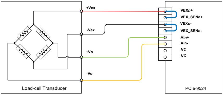
A load-cell is comprised of four resistive strain-gauges connected in Wheatstone bridge form, and is inherently a floating differential output device. Since a load-cell transducer is a passive device, it requires voltage excitation in order to transform the resistive change into electrical signals. A typical four-wire connection is shown on Figure 3-4.

Figure 3-4: Connecting to a four-terminal load-cell transducer using a four-wire connection
![+Vex\n-Vex\n+Vo\n-Vo\nLoad-cell Transducer\nPCIe-9524\nVEXn+\nVEX_SENn+\nVEXn-\nVEX_SENn-\nAln+\nAln-\nNC\nNC](.pcie-9524-um-v1-0/2c0c23a7b3d38bb97a79b2357c78e025cbdfb204669bd59f9d04127000910c9b.jpg)

It is recommended to enable the remote-sense function, and loopback the VEXn+/- to VEX\_SENn+/- on the terminal board you're using when connecting to the transducer. A lengthy extension cable between PCIe-9524 and the terminal board inevitably has some lead resistance that results in voltage drop; looping-back the excitation on the terminal board creates a six-wire connection and compensates for voltage drop.

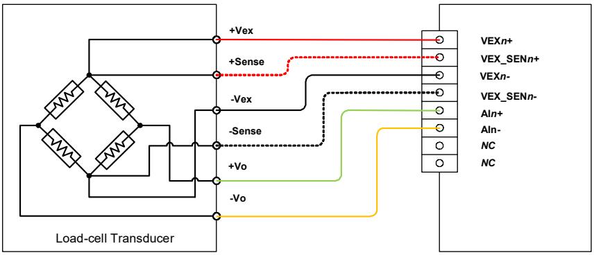
A better approach is to use specially designed load-cell transducers having two additional SENSE terminals. The voltage difference across the bridge excitation junctions is fed back to the voltage excitation circuitry by two separate 'sense-wires', to further correct the voltage drops due to the resistance in the excitation wiring. Be sure to enable the remote-sense function to take full advantage of a six-wire connection. A typical six-wire connection is shown in Figure 3-5.

Figure 3-5: Connecting to a six-terminal load-cell transducer using a six-wire connection
![The diagram shows a wiring schematic connecting a 'Load-cell Transducer' to a connector interface.\n\n**Left Block (Load-cell Transducer):**\nThis block contains a Wheatstone bridge circuit and lists the following terminal labels from top to bottom:\n*   +Vex\n*   +Sense\n*   -Vex\n*   -Sense\n*   +Vo\n*   -Vo\n*   Load-cell Transducer (Label at the bottom)\n\n**Right Block (Connector Interface):**\nThis block features a vertical column of pins with the following labels to the right, from top to bottom:\n*   VEXn+\n*   VEX_SENn+\n*   VEXn-\n*   VEX_SENn-\n*   AIn+\n*   AIn-\n*   NC\n*   NC\n\n**Connections:**\n*   A red solid line connects **+Vex** to **VEXn+**.\n*   A red dashed line connects **+Sense** to **VEX_SENn+**.\n*   A black solid line connects **-Vex** to **VEXn-**.\n*   A black dashed line connects **-Sense** to **VEX_SENn-**.\n*   A green solid line connects **+Vo** to **AIn+**.\n*   A yellow solid line connects **-Vo** to **AIn-**.](.pcie-9524-um-v1-0/0e6eb278e210b53ac208c80501056350b87498dbfa50313a758607200e0398d2.jpg)

Whether to use a six-wire connection is dependent on the impedance of the load-cell transducers you are using, length of the wiring cable, wire-gauge inside the cable, and the required measurement accuracy. We recommend you to use a six-wire connection as the default connection method for high-accuracy load-cell transducers.

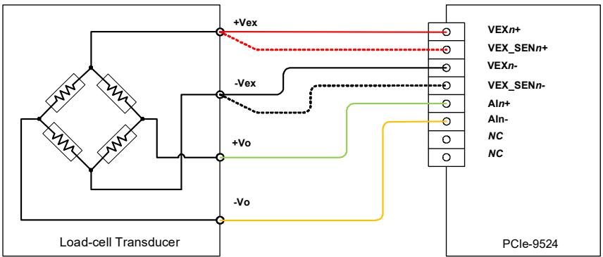
To add remote-sense capability to a four-terminal load-cell transducer, simply run two separate sense-wires, and join them together with the excitation wires at the transducer's excitation terminals.

Figure 3-6: Connecting to a four-terminal load-cell transducer using a six-wire connection
![**Blocks:**\n*   **Load-cell Transducer**: A block on the left containing a Wheatstone bridge circuit with four resistors arranged in a diamond shape.\n*   **PCIe-9524**: A block on the right representing a module with a vertical column of connection terminals.\n\n**Connections:**\n*   **From Load-cell Transducer to PCIe-9524:**\n    *   The top vertex of the bridge connects to a node labeled **+Vex**. From this node, a solid red wire connects to **VEXn+** and a dashed red wire connects to **VEX_SENn+**.\n    *   The left vertex of the bridge connects to a node labeled **-Vex**. From this node, a solid black wire connects to **VEXn-** and a dashed black wire connects to **VEX_SENn-**.\n    *   The right vertex of the bridge connects to a node labeled **+Vo**. From this node, a solid green wire connects to **AIIn+**.\n    *   The bottom vertex of the bridge connects to a node labeled **-Vo**. From this node, a solid yellow wire connects to **AIIn-**.\n*   **Internal to PCIe-9524:** The remaining two terminals at the bottom are labeled **NC**.](.pcie-9524-um-v1-0/7a77ef1c28e392c2d788c1be8d17908c1df17e642e0774ec594b3f3ac6729208.jpg)

# Differential input mode for general purpose input channels

AI channels 4 to 7 are designed for connecting to ground-referenced or floating sources in differential mode.

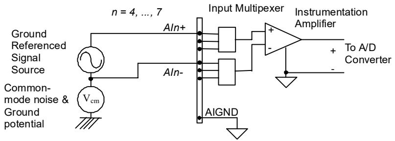
The differential input mode provides two inputs that respond to signal voltage difference between them. If the signal source is ground-referenced, the differential mode can be used for the common-mode noise rejection. Figure 3-7 presents an example of ground-referenced signal source connections under differential input mode.

Figure 3-7: Ground-referenced source and differential input
![Based on the provided flowchart/block diagram, here is the accurate description of the labeled blocks and connections:\n\n**Labeled Blocks and Components:**\n*   **Left Side:**\n    *   Text: 'Ground Referenced Signal Source' next to an AC voltage source symbol (circle with a sine wave).\n    *   Text: 'Common-mode noise & Ground potential' next to a DC voltage source labeled 'V_cm' connected to ground.\n*   **Middle Section:**\n    *   Text: 'n = 4, ..., 7' positioned above the top signal line.\n    *   Text: 'AIn+' labeling the top signal line.\n    *   Text: 'AIn-' labeling the middle signal line.\n    *   Text: 'AIGND' labeling the bottom signal line connected to ground.\n    *   A vertical bar with a column of dots, labeled at the top as 'Input Multiplexer'.\n    *   Two rectangular blocks positioned to the right of the vertical bar.\n*   **Right Side:**\n    *   A triangle symbol labeled 'Instrumentation Amplifier'.\n    *   Text: 'To A/D Converter' positioned at the output.\n\n**Connections:**\n1.  **Signal Source:** The top terminal of the AC source connects to the line labeled '**AIn+**'. The bottom terminal of the AC source connects to the top terminal of the DC source '**V_cm**' and also to the line labeled '**AIn-**'. The bottom of 'V_cm' connects to ground.\n2.  **Multiplexer Inputs:**\n    *   The '**AIn+**' line connects to the top-most dot on the vertical bar of the '**Input Multiplexer**'.\n    *   The '**AIn-**' line connects to the second dot down on the vertical bar.\n    *   The bottom dot on the vertical bar connects to the line labeled '**AIGND**', which goes to a ground symbol.\n3.  **Multiplexer Outputs to Amplifier:**\n    *   Lines from the upper portion of the vertical bar connect to the left side of the top rectangular block. The output of this block connects to the non-inverting ('+') input of the '**Instrumentation Amplifier**'.\n    *   Lines from the lower portion of the vertical bar connect to the left side of the bottom rectangular block. The output of this block connects to the inverting ('-') input of the '**Instrumentation Amplifier**'.\n4.  **Amplifier Output:**\n    *   The output terminal labeled '+' of the amplifier connects to the text '**To A/D Converter**'.\n    *   The output terminal labeled '-' is connected to a ground symbol.](.pcie-9524-um-v1-0/8d900e4a48b3d20c1fd5cd6b9bd4cb3567f1a11bb52550d4795acf1c7dca8ee6.jpg)

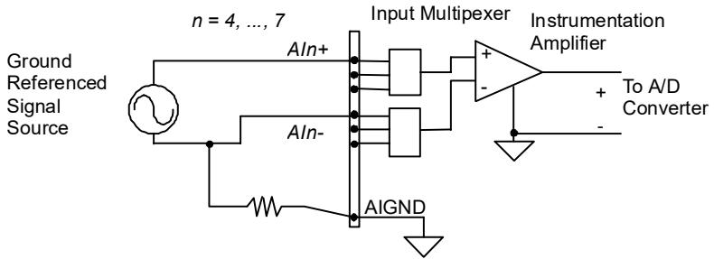
Figure 3-8 shows how to connect a floating signal source to PCIe-9524 in differential input mode. For floating signal sources, you need to add a resistor at each channel to provide a bias return path. The resistor value should be about 100 times the equivalent source impedance. If the source impedance is less than 100, you can simply connect the negative side of the signal to AIGND as well as the negative input of the Instrumentation Amplifier without any resistors. In differential input mode, less noise couples into the signal connections than in single-ended mode.

Figure 3-8: Floating source and differential input
![n = 4, ..., 7\nGround\nReferenced\nSignal\nSource\nAln+\nInput Multipexer\nInstrumentation\nAmplifier\nAln-\nTo A/D\nConverter\nAIGND](.pcie-9524-um-v1-0/93f878bb31571765776b9b60630c4b2f4c5c995b1be83b0e08e21bc1e6a55a5a.jpg)

# 3.3 Isolated Digital Signal Connection

PCIe-9524 provides three opto-isolated encoder input channels, three opto-isolated pulse-command outputs, eight channel optoisolated digital inputs as well as eight channel isolated digital outputs. Also, a built-in isolated power supply can be used as a resistors pull-up source.

# 3.3.1 Signal Sources and Terminal Devices

# Open-collector and open-drain outputs

Open-collector or open-drain output stages are commonly used in industrial I/O. Open-collector/open-drain output stages made of NPN or N-MOS type transistors are for sink-type drivers, while those made of PNP or P-MOS type are for source-type drivers. A sink-driver sinks current from the external pull-up resistor when it is activated, and floats when it is inactivated; conversely, a sourcedriver sources current to the external pull-down resistor when it is activated, and floats when it is inactivated. High-side voltage can usually go as high as the output transistor can tolerate, and hence offers a wider, more versatile output voltage selection. The drawback is that when the output stage is inactivated, either the signal fall-time of a source-driver or the rise-time of a sink-driver, is determined by the RC time-constant formed by the pull-up/pull-down resistor and the stray capacitance. The asymmetrical rise/fall-time somehow limits the frequency response of the output stage.

# Push-pull outputs

Push-pull output stages are comprised of a complementary transistor pair, say, a PNP plus a PNP, or a P-MOS plus an N-MOS. Unlike open-collector output stages, they can sink or source current and hence a symmetrical rise/fall-time that is independent of the external load resistance. Push-pull output stages can generally toggle at a much faster speed than open-collector output stages.

# Line-driver outputs

A Line-driver output stage is of differential output type, providing a normal output and a complementary output for each signal port. A Line-driver usually works at a much lower supply voltage and can toggle quickly. By utilizing differential transmission topology, the transmission distance can be extended considerably and with relatively low EMI.

The line-driver used on PCIe-9524 is of voltage-driving type AM26LS31, compliant with ANSI TIA/EIA-422-B requirements. Either one of the two complementary outputs can be regarded as a single-ended push-pull output, and can be connected to an optoisolated input or a TTL input.

# Opto-coupler Inputs

Opto-coupler inputs are of current input type devices, made of a light-emitting-diode (LED) and an integrated light-sensitive transistor. They accept wide input voltage ranges, provided that the input current is limited by a series external resistor in order to protect the integrated LED device.

# Line-receiver inputs

The line-receiver, as its name implies, is used to accept signals from line-drivers. It's of differential input type, providing a normal input and a complementary input for each signal port.

![This image displays a white document icon with a folded upper-right corner. Faint gray horizontal lines run across the page to represent text. A large, bold red checkmark with a slightly rough, brush-like texture is superimposed over the center of the document.](.pcie-9524-um-v1-0/59dc5afe0a7f6d1fe8db37a1bdeebc94e75b193e2880beca9529707b9708495f.jpg)
NOTE:

1) The isolated ground (ISOGND) is shared between all isolated functions in PCIe-9524. Make sure the ISOGND is connected to a known ground potential, only at one point in the system.
2) Do not let the ISOGND float, nor connect it directly to a chassis, as it may cause EMI and/or accumulate a charge that lead to safety hazards.
3) Shield the exposed ISOGND pins, connectors, and wiring, if possible to run a ground potential that is greater then 30-VDC.
4) Do not connect the ISOGND to analog ground (AGND), the noise on ISOGND will ruin analog performance.

# 3.3.2 Connecting to/from External Encoders

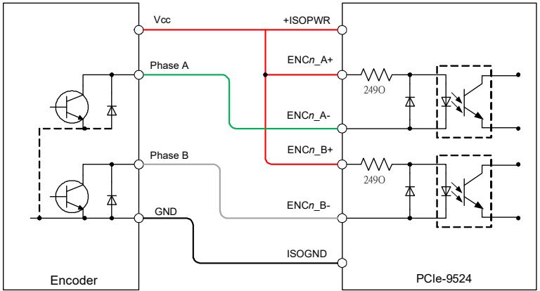
Figure 3-9: Connecting to an external encoder with NPN sink drivers
![The block diagram depicts two main labeled blocks: **Encoder** and **PCIe-9524**.\n\nThe connections between the labeled terminals are as follows:\n*   **Vcc** connects to **+ISOPWR**, **ENCn_A+**, and **ENCn_B+**.\n*   **Phase A** connects to **ENCn_A-**.\n*   **Phase B** connects to **ENCn_B-**.\n*   **GND** connects to **ISOGND**.](.pcie-9524-um-v1-0/a8fee1ae53a7f0a723114448cf35a850807674fc3832e55273ed1a1094dab6d3.jpg)

Figure 3-10: Connecting to an external encoder with PNP source drivers
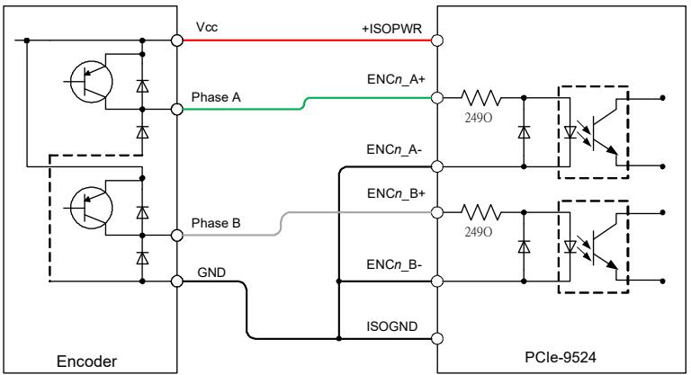
![The diagram illustrates a connection between two main blocks: an **Encoder** block on the left and a **PCIe-9524** block on the right.\n\n**Connections between blocks:**\n*   A red line labeled **Vcc** connects the top terminal of the Encoder block to the **+ISOPWR** terminal of the PCIe-9524 block.\n*   A green line labeled **Phase A** connects a terminal in the Encoder block to the **ENCn_A+** terminal of the PCIe-9524 block.\n*   A grey line labeled **Phase B** connects a terminal in the Encoder block to the **ENCn_B+** terminal of the PCIe-9524 block.\n*   A black line labeled **GND** connects the bottom terminal of the Encoder block to the **ISOGND** terminal of the PCIe-9524 block.\n\n**Internal connections within the PCIe-9524 block:**\n*   The **ENCn_A-** terminal connects directly to the **ENCn_B-** terminal and the **ISOGND** terminal.\n*   **Signal Path A:** The **ENCn_A+** terminal connects to a resistor labeled **249Ω**. Following the resistor, the line splits:\n    *   One path goes through a diode (pointing downward) to the **ENCn_A-** terminal.\n    *   The other path connects to a dashed box containing a phototransistor symbol (arrow pointing outward). The emitter of this phototransistor connects to the **ENCn_A-** terminal, and the collector connects to an output terminal (represented by a dot on the far right).\n*   **Signal Path B:** Similarly, the **ENCn_B+** terminal connects to a resistor labeled **249Ω**. Following the resistor, the line splits:\n    *   One path goes through a diode (pointing downward) to the **ENCn_B-** terminal.\n    *   The other path connects to a dashed box containing a phototransistor symbol (arrow pointing outward). The emitter connects to the **ENCn_B-** terminal, and the collector connects to an output terminal on the far right.](.pcie-9524-um-v1-0/4c97a03a6263021347ae20a65313cdefc48121e6b56332d52cd08f57c9d74b8b.jpg)

Figure 3-11: Connecting to an external encoder with push-pull source drivers
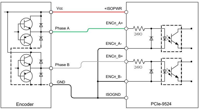
![**Labeled Blocks:**\n*   **Encoder**\n*   **PCIe-9524**\n\n**Connections:**\n*   **Power:** A red wire labeled **Vcc** connects to a terminal labeled **+ISOPWR**.\n*   **Signal A:** A green wire labeled **Phase A** connects to a terminal labeled **ENCn_A+**. From this terminal, the signal passes through a resistor labeled **249Ω** and connects to the input of a diode and an optocoupler (dashed box), which then connect to a terminal labeled **ENCn_A-**.\n*   **Signal B:** A grey wire labeled **Phase B** connects to a terminal labeled **ENCn_B+**. From this terminal, the signal passes through a resistor labeled **249Ω** and connects to the input of a diode and an optocoupler (dashed box), which then connect to a terminal labeled **ENCn_B-**.\n*   **Ground:** The terminals **ENCn_A-** and **ENCn_B-** are shorted together and connect to a terminal labeled **ISOGND**. A black wire labeled **GND** connects to **ISOGND**.](.pcie-9524-um-v1-0/9874fcce07a76f8a0f7ff26e333855fd74594ec9c8f3ae380a04149037b99dcc.jpg)

Figure 3-12: Connecting to an external encoder with differential line-drivers
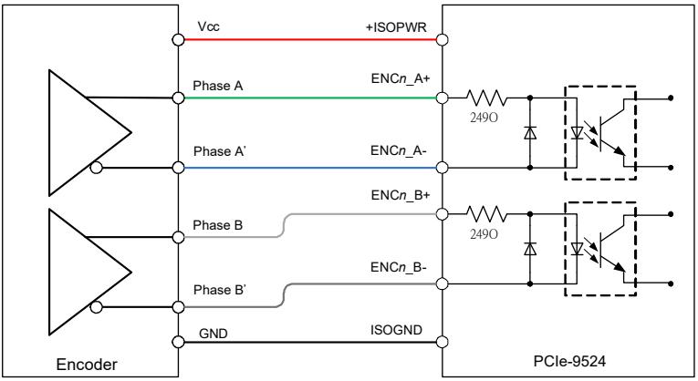
![This diagram illustrates the connection between an **Encoder** block on the left and a **PCIe-9524** block on the right.\n\n**Labeled Blocks:**\n*   **Encoder**: Contains two triangle symbols (buffers/inverters) with outputs labeled **Phase A**, **Phase A'**, **Phase B**, and **Phase B'**, along with power inputs **Vcc** and **GND**.\n*   **PCIe-9524**: Contains input terminals labeled **+ISOPWR**, **ENCn_A+**, **ENCn_A-**, **ENCn_B+**, **ENCn_B-**, and **ISOGND**, along with internal circuitry including resistors, diodes, and optocouplers.\n\n**Connections:**\n*   **Power**: **Vcc** from the Encoder connects to **+ISOPWR** on the PCIe-9524. **GND** from the Encoder connects to **ISOGND** on the PCIe-9524.\n*   **Channel A**:\n    *   **Phase A** connects to **ENCn_A+**.\n    *   **Phase A'** connects to **ENCn_A-**.\n*   **Channel B**:\n    *   **Phase B** connects to **ENCn_B+**.\n    *   **Phase B'** connects to **ENCn_B-**.\n\n**Internal Circuitry (within PCIe-9524):**\n*   **Resistors**: Each channel (**ENCn_A+** and **ENCn_B+**) connects to a resistor labeled **249Ω**.\n*   **Protection/Isolation**: The output of each resistor connects to a node shared by:\n    *   A pair of bidirectional diodes (TVS/clamp).\n    *   The LED input of an optocoupler (shown inside a dashed box).\n    *   The other side of the diodes and LED connects to the respective return line (**ENCn_A-** or **ENCn_B-**).\n*   **Outputs**: The phototransistor output of each optocoupler connects to external terminals (indicated by black dots).](.pcie-9524-um-v1-0/016689305cf0cee0f6dde9332e66557188b7a8751704695a637f5e56a154c184.jpg)

# 3.3.3 Connecting to External Servo Amplifiers

Figure 3-13: Connecting to an external servo-amplifier with opto-coupler inputs
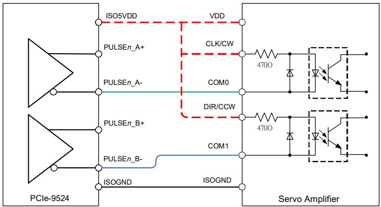
![Based on the provided flowchart/block diagram, here is an accurate and concise description:\n\n**Blocks:**\n*   **PCle-9524** (Left block)\n*   **Servo Amplifier** (Right block)\n\n**Connections:**\n*   **Left to Right Connections:**\n    *   **ISO5VDD** connects to **VDD** via a red dashed line.\n    *   **PULSE_n_A+** connects to **CLK/CW**.\n    *   **PULSE_n_A-** connects to **COM0** via a green line.\n    *   **PULSE_n_B+** connects to **DIR/CCW**.\n    *   **PULSE_n_B-** connects to **COM1** via a blue line.\n    *   **ISOGND** connects to **ISOGND**.\n\n*   **Internal Connections within Servo Amplifier:**\n    *   **VDD** connects to the input lines for **CLK/CW** and **DIR/CCW** via a vertical red dashed line.\n    *   **Top Circuit:** The **CLK/CW** line connects to a **4700** resistor. The output of the resistor connects to a node where a diode (pointing down) and an LED (optocoupler input) connect. The diode cathode and the transistor (optocoupler output) emitter connect to **COM0**. The transistor collector connects to the LED cathode. The transistor emitter connects to an output pin.\n    *   **Bottom Circuit:** The **DIR/CCW** line connects to a **4700** resistor. The output of the resistor connects to a node where a diode (pointing down) and an LED connect. The diode cathode and the transistor emitter connect to **COM1**. The transistor collector connects to the LED cathode. The transistor emitter connects to an output pin.](.pcie-9524-um-v1-0/22a3e7866090e62812f322e0d87098f912f524f1c9934fb2bba864773ef16da8.jpg)

Figure 3-14: Connecting to an external servo-amplifier with differential line-receivers
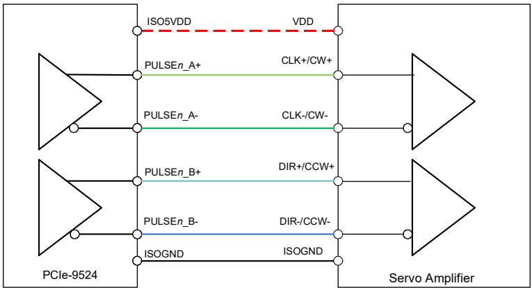
![The image is a block diagram illustrating the connection between two devices:\n\n**Labeled Blocks:**\n*   **PCIe-9524** (Left block)\n*   **Servo Amplifier** (Right block)\n\n**Connections:**\nThere are six horizontal lines connecting the two blocks, labeled as follows:\n\n1.  **ISO5VDD** (left) connects to **VDD** (right) via a red dashed line.\n2.  **PULSEn_A+** (left) connects to **CLK+/CW+** (right) via a green solid line.\n3.  **PULSEn_A-** (left) connects to **CLK-/CW-** (right) via a green solid line.\n4.  **PULSEn_B+** (left) connects to **DIR+/CCW+** (right) via a cyan solid line.\n5.  **PULSEn_B-** (left) connects to **DIR-/CCW-** (right) via a blue solid line.\n6.  **ISOGND** (left) connects to **ISOGND** (right) via a black solid line.\n\n**Internal Components:**\n*   Inside the **PCIe-9524** block, there are four triangular buffer symbols. The outputs for the negative signals (**PULSEn_A-** and **PULSEn_B-**) include a small circle, indicating inversion.\n*   Inside the **Servo Amplifier** block, there are four triangular buffer symbols. The inputs for the negative signals (**CLK-/CW-** and **DIR-/CCW-**) include a small circle, indicating inversion.](.pcie-9524-um-v1-0/49bab69dfafe1edf98f0800b59503aa34cbd73e6bfc56266c6e88433e6ad48da.jpg)

# 3.3.4 Interfacing Isolated DO with External Loads Connecting to external resistive loads

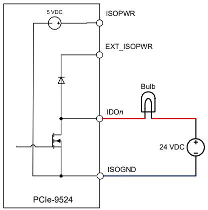
Figure 3-15 presents connecting to external resistive loads. The left side illustrates driving an external LED using the internal ISOPWR source; the right side illustrates driving an external 5W, 24-VDC Bulb using an external power supply.

Figure 3-15: Connecting to an external resistive load from the isolated DO sink driver
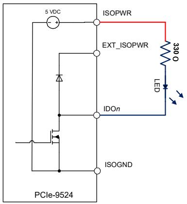
![5 VDC\nISOPWR\nEXT_ISOPWR\n330 Ω\nLED\nIDOn\nISOGND\nPCIe-9524](.pcie-9524-um-v1-0/624a0d08dce555accd8ace889bd24678b331bbdc2a8244deeeb6a8f40a19e9bc.jpg)

![5 VDC\nISOPWR\nEXT_ISOPWR\nIDOn\nBulb\n24 VDC\nPCle-9524\nISOGND](.pcie-9524-um-v1-0/6c45d951b54b857b61e9e8a995f8b50c3cbe70a893b87c673b0977f077cba8e0.jpg)

# Connecting to external inductive loads

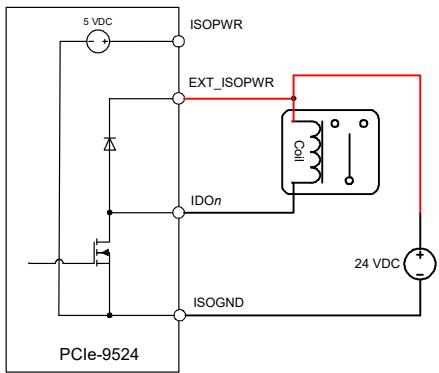
Figure 3-16 presents connecting to external resistive loads. The left side illustrates driving a 5-VDC relay coil using the internal ISOPWR source; the right side illustrates driving an external 12- VDC relay coil using an external power supply.

Figure 3-16: Connecting to an external inductive load from an isolated DO sink driver
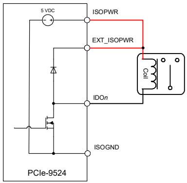
![5 VDC\nISOPWR\nEXT_ISOPWR\nIDOn\nISOGND\nPCIe-9524](.pcie-9524-um-v1-0/dd8f329c16d3323130acc0ac13deac1aca65777ec87e45bdbe8dbe6f0afd5201.jpg)

![5 VDC\nISOPWR\nEXT_ISOPWR\nIDOn\n24 VDC\nPCle-9524\nISOGND](.pcie-9524-um-v1-0/7e03758565a828714590baae1638bae41ce8560938e772cdc28e1619986d26a8.jpg)

# 3.3.5 Interfacing Isolated DI with External Devices Connecting to a low-side push button

Alternatively, the push button can be connected at the high-side, i.e. between the ISOVDD and IDn+ pins. Also, the IDIn+ and IDIncan be interchanged, since the opto-coupler accepts bipolar input signals.

Figure 3-17: Connecting to a low-side push button
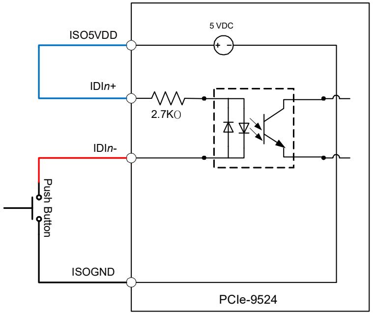
![ISO5VDD\nIDIn+\n2.7KO\nIDIn-\nPush Button\nISOGND\n5 VDC\nPCIe-9524](.pcie-9524-um-v1-0/2c6fb6fed111e4c143395bdcf822dd0adf034e19bd365f77685454c010cb367b.jpg)

# Connecting to an external sink driver

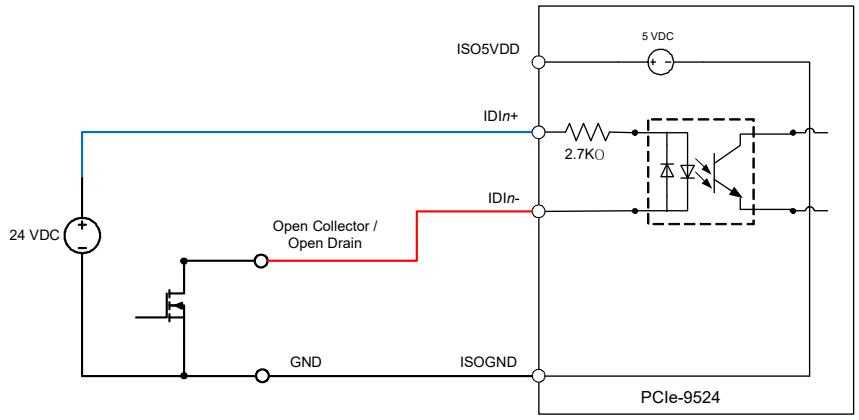
The sink driver can also be replaced by a mechanical switch, a proximity-sensor, etc. An external power-supply can be used instead of the internal isolated power source.

Figure 3-18: Connecting to an external sink driver
![24 VDC\nOpen Collector / Open Drain\nGND\nISOGND\nISO5VDD\nIDIn+\n2.7KΩ\nIDIn-\n5 VDC\nPCIe-9524](.pcie-9524-um-v1-0/303dde84fdd31e3b3ba3fd2c75fe474b90f0ccbf672a87bc1ac60b52f6fa5fb7.jpg)

# 4 Operation Theory

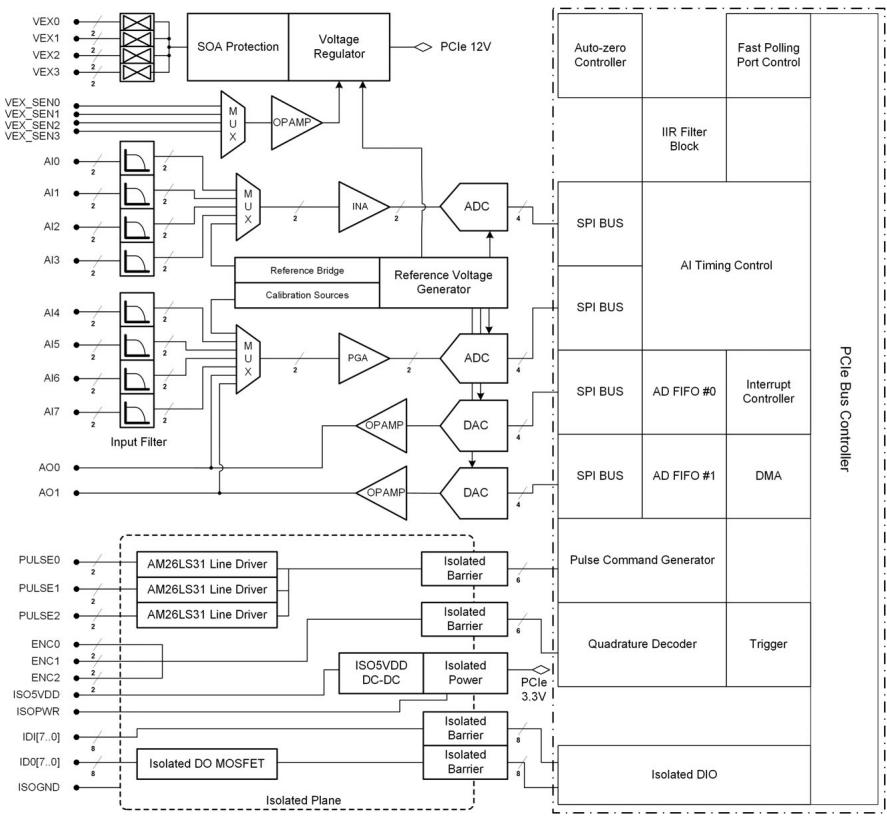
The operation theory of the functions of PCIe-9524 are described in this chapter. The functions include A/D conversion, D/A conversion, pulse-commands, encoder inputs, and isolated digital I/O. Operation theory helps users understand how to configure and program PCIe-9524.

# 4.1 PCIe-9524 Function Diagram

Figure 4-1: PCIe-9524 Function Diagram
![**Labeled Blocks:**\n*   **Inputs:** VEX0, VEX1, VEX2, VEX3; VEX_SEN0, VEX_SEN1, VEX_SEN2, VEX_SEN3; AI0, AI1, AI2, AI3; AI4, AI5, AI6, AI7; AO0, AO1; PULSE0, PULSE1, PULSE2; ENC0, ENC1, ENC2; IS0VDD, ISOPWR, ISOGND; IDI(7..0); IDQ(7..0).\n*   **Processing/Control Blocks:** SOA Protection; Voltage Regulator; MUX; OPAMP; Input Filter; INA; ADC; Reference Bridge; Calibration Sources; Reference Voltage Generator; PGA; DAC; AM26LS31 Line Driver; Isolated Barrier; ISO5VDD DC-DC; Isolated Power; Isolated DO MOSFET; Auto-zero Controller; Fast Polling Port Control; IIR Filter Block; AI Timing Control; SPI BUS; AD FIFO #0; Interrupt Controller; AD FIFO #1; DMA; Pulse Command Generator; Quadrature Decoder; Trigger; Isolated DIO.\n*   **Outputs/Labels:** PCle 12V; PCle 3.3V; PCIe Bus Controller; Isolated Plane.\n\n**Connections:**\n*   **Power Section:** VEX0, VEX1, VEX2, and VEX3 connect to a transformer symbol, which connects to 'SOA Protection'. 'SOA Protection' connects to the 'Voltage Regulator'. The 'Voltage Regulator' outputs 'PCle 12V'. VEX_SEN0, VEX_SEN1, VEX_SEN2, and VEX_SEN3 connect to a 'MUX', which connects to an 'OPAMP', which connects back to the 'Voltage Regulator'.\n*   **Analog Input Path (AI0-AI3):** AI0, AI1, AI2, and AI3 connect to an 'Input Filter'. The output connects to a 'MUX', which connects to an 'INA'. The 'INA' output connects to an 'ADC'.\n*   **Reference Path:** 'Reference Bridge' and 'Calibration Sources' connect to a 'Reference Voltage Generator', which connects to the 'ADC'.\n*   **Analog Input Path (AI4-AI7) & DAC Path:** AI4, AI5, AI6, and AI7 connect to an 'Input Filter'. The output connects to a 'MUX', which connects to a 'PGA'. The 'PGA' output connects to an 'ADC'. This 'ADC' connects to a 'DAC'.\n*   **Output Path (AO0/AO1):** AO0 connects to an 'OPAMP', which connects to a 'DAC'. AO1 connects to an 'OPAMP', which connects to a 'DAC'.\n*   **Digital/Pulse Section (Isolated Plane):** A dashed box labeled 'Isolated Plane' encloses the following: PULSE0, PULSE1, PULSE2 connect to 'AM26LS31 Line Driver' blocks. The drivers connect to 'Isolated Barrier' blocks. ENC0, ENC1, ENC2 connect to 'ISO5VDD DC-DC', which connects to 'Isolated Power'. 'Isolated Power' outputs 'PCle 3.3V'. IS0VDD, ISOPWR, and ISOGND connect to 'Isolated Power'. IDI(7..0) connects to 'Isolated DO MOSFET', which connects to an 'Isolated Barrier'. IDQ(7..0) connects to the same 'Isolated Barrier'.\n*   **PCIe Bus Controller:** A large vertical block labeled 'PCIe Bus Controller' contains sub-blocks including 'Auto-zero Controller', 'Fast Polling Port Control', 'IIR Filter Block', 'AI Timing Control', 'SPI BUS', 'AD FIFO #0', 'Interrupt Controller', 'AD FIFO #1', 'DMA', 'Pulse Command Generator', 'Quadrature Decoder', 'Trigger', and 'Isolated DIO'. The 'SPI BUS' blocks connect to the ADCs and DACs. The 'Pulse Command Generator' and 'Quadrature Decoder' receive inputs from the isolated barriers. The 'Isolated DIO' connects to the bottom isolated barriers.](.pcie-9524-um-v1-0/a27af65558f3289215a52295eb364c5278ee793b4f498741f0795bef876cd2c2.jpg)

# 4.2 Analog Input Channels

The following sub-sections depict the internal operations of signal amplification, conversion, post-processing, and calibration.

# 4.2.1 Signal Acquisition and Processing Flow

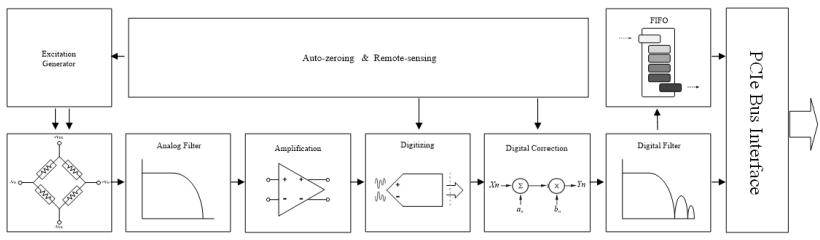
PCIe-9524 was designed to detect weak signals through proper signal conditioning, amplification and digital post filtering, as depicted.

Figure 4-2: Signal acquisition and data processing flow for transducer input channels
![**Labeled Blocks:**\n*   Excitation Generator\n*   Auto-zeroing & Remote-sensing\n*   FIFO\n*   PCIe Bus Interface\n*   Analog Filter\n*   Amplification\n*   Digitizing\n*   Digital Correction\n*   Digital Filter\n\n**Connections:**\n*   **Excitation Generator** connects left to **Auto-zeroing & Remote-sensing**.\n*   **Excitation Generator** connects downward to a Wheatstone bridge circuit schematic.\n*   **Auto-zeroing & Remote-sensing** connects downward to **Digitizing**.\n*   **Auto-zeroing & Remote-sensing** connects downward to **Digital Correction**.\n*   **FIFO** connects right to **PCIe Bus Interface**.\n*   **Digital Filter** connects upward to **FIFO**.\n*   The bottom row follows a left-to-right flow: The Wheatstone bridge schematic connects to **Analog Filter**, which connects to **Amplification**, which connects to **Digitizing**, which connects to **Digital Correction**, which connects to **Digital Filter**.](.pcie-9524-um-v1-0/3825a0deb262e66515330b9efea1d49e481ec2221ce1f1d491df49351289b835.jpg)

At the first stage, the voltage excitation applied to the load-cell transducer transforms the resistive change into an electric signal, in the range of tens of milli-volts. Before entering amplification stage, the signal passes through a passive filter stage to filter out unwanted interference. A custom-made, low temperature coefficient instrumentation amplifier provides a fixed gain of 25, and the necessary level-shift (1). The amplified signal is fed into a sigmadelta modulator running at 1.92 MHz, pushing the in-band quantization noise to a higher frequency, and filtering most of which out using a 5-order SINC filter. The filtered digital data passes through an averager to tune down the data rate to a specific sampling rate. A built-in correction algorithm automatically calibrates the output data, which can then be pushed into the on-board FIFO for data transfer to PC memory, or sent to the next DSP stage described below.

There are four programmable post-processing IIR digital filter banks (2), one for each load-cell transducer input channel. Each bank is a fixed-coefficient, variable-length IIR digital filter, and can be instructed to flush itself once a large input-step is observed. The processed data are pushed into the on-board FIFO for DMA data transfer to PC memory; otherwise, they are read by user applications directly, without buffering, through fast-polling data transfers.

The software driver utilizes a look-up-table to correct the null offset and gain error of the analog front-end, using a built-in 1.25k bridge, to provide adequate absolute accuracy for applications that do not calibrate load-cell transducers in the field. For applications that always perform null and gain calibrations in the field, users can manipulate the 2's complementary binary code directly.

Throughout the acquisition and processing flow, remote-sensing (3) and auto-zeroing (4) are working simultaneously to compensate voltage drops over excitation wires, and to remove thermal drift and 1/f noise in signal paths. The dynamic error compensation is essential to achieve high-stability measurements; otherwise the output will drift at a very low frequency that is difficult to be reconstructed using any other post-filtering method.

![The image displays a vertical icon featuring a white document with horizontal lines. A large red checkmark is drawn across the document. Below the graphic, the text 'NOTE-' is written in black capital letters.](.pcie-9524-um-v1-0/a0f790d203d9cb9b2f023b06cf22cd8055b0fd45ab187825c331e641142f9090.jpg)

1) For general purpose analog input channels, i.e. channels 4 to 7, the available gain ranges are 1, 2, 4, and 8.
2), 3), 4) The general purpose analog input channels, i.e. channel 4 to 7, do not support the remote-sensing and auto-zeroing functions.

# 4.2.2 How to Define a 1 in 200,000 Count Resolution

It is common in the weight-scaling or material-testing industries to specify the resolution capability of a measurement device such as PCIe-9524, in Counts or Digits, rather than in bits.

For example, a measurement device that is capable of resolving 1 in 1000 counts, can successfully register a 1-gram change on a 1- kg capacity load-cell transducer. Consequently, a measurement device that is capable of resolving 1 in 200,000 counts, can successfully register a 1-gram change on a 200-kg capacity load-cell transducer.

In practical applications, the sensitivity of load-cell transducers vary from model to model (typically form 1 to 4mV/V), and the fullscale output range of a transducer is usually only a fraction of the full-scale input range of a measurement device. The convenience of using Counts rather than Bits, is that the specified Count achievable by a measurement device, is relative to the transducers full-scale output, rather than the full-scale input range of the analog input amplifier. Thus, theoretically, no matter what the sensitivity of the 200-kg capacity load-cell transducer you are using, a 200,000 count measurement device can always resolve a 1-gram measurement.

Please also note, as a weight/force indicator, the displayed Counts or Digits shall be flicker-free while the applied force is in steady state. Therefore, a measurement device specified to have a 200,000 count resolution, must guarantee peak-to-peak system noise and short-term drift to below 1 / 200,000, or 5-ppm of the full-scale output range of the transducer.

The specified 200,000 count resolution capacity of PCIe-9524 is verified by a precision load-cell simulator utilizing 3mV/V sensitivity, under 10-V excitation and using a six-wire remote-sense connection. The auto-zero function is enabled throughout acquisition, while the ADC sampling rate is set to 60 samples-per-second (the equivalent data rate is 29 samples-per-second, see Section 4.2.3 for details), and using an IIR post digital filter of 32-taps (see Section 4.2.9 for details). Under these conditions, the peak-topeak system noise and drift are well below 150-nano-Volts, the limit of 1 in 200,000 count resolution. The recording duration is 30 minutes, and the ambient temperature fluctuation is within ± 1ºC throughout.

# 4.2.3 Data Rate versus Sampling Rate

Due to the internal delay time and manipulations required for autozeroing and remote-sensing functions, the 'Sampling Rate' that the ADC is actually running at can be different from the actual 'Data Rate'.

In the following sections, the term 'Sampling Rate' and 'Data Rate' are of different meaning. The 'Sampling Rate' stands for the ADC's internal conversion speed set by users, whereas the 'Data Rate' stands for the output rate of the processed data.

See Table 4-1 for equivalent data rates versus ADC actual sampling rates, under different operating modes. When programming through a software API, users must set the desired ADC sampling rate, and the actual 'Data Rate' will be looked-up and returned by the software API for your reference.

# 4.2.4 Auto-scan, Multiplexing and Settling Time

PCIe-9524 uses multiplexing for transducer input channels, and up to four transducers can be attached. When the Auto-scan feature is enabled, the hardware multiplexes and scans the four transducers in sequence; AI0, AI1, AI2, AI3, and AI0…etc.

Multiplexing increases the number of transducers that a single amplifier can deal with, it does however require additional time for the signal to rise/fall and propagate through the circuit stages. The time delay therefore required is called 'Settling Time'. Besides the propagation delay within PCIe-9524, the parasitic in the cabling, the impedance of the transducers, and the amplitude difference between channels, affect final settling time figures.

PCIe-9524 is programmed to have 400-µs default settling time, and this works best with low impedance transducers, such as 120 or 350-ohm load-cells. Insufficient settling time may causes interchannel crosstalk; the new signal will not be able to fully settle to its final value, and some 'residual' signals in the previous measurement will be present in the current measurement. Users may increase the hardware settling time, to check if a lesser inter-channel crosstalk is perceived. See Table 4-1 for the equivalent Data Rates versus ADC actual Sampling Rates, under different operating modes.

Table 4-1: Data Rates vs. Multiplexing, Auto-zero & ADC Sampling Rates, in Samples-per-second (SPS)

<table><tr><td rowspan="2">ADC Sampling Rate</td><td colspan="2">Non-multiplexed</td><td colspan="2">Multiplexed</td></tr><tr><td>Auto-zero Disabled</td><td>Auto-zero Enabled</td><td>Auto-zero Disabled</td><td>Auto-zero Enabled</td></tr><tr><td>30,000</td><td>30,000</td><td>818.73</td><td>1637.47</td><td>818.73</td></tr><tr><td>15,000</td><td>15,000</td><td>768.40</td><td>1536.81</td><td>768.40</td></tr><tr><td>7,500</td><td>7,500</td><td>703.53</td><td>1407.06</td><td>703.53</td></tr><tr><td>3,750</td><td>3,750</td><td>594.74</td><td>1189.48</td><td>594.74</td></tr><tr><td>2,000</td><td>2,000</td><td>462.66</td><td>925.33</td><td>462.66</td></tr><tr><td>1,000</td><td>1,000</td><td>316.32</td><td>632.63</td><td>316.32</td></tr><tr><td>500</td><td>500</td><td>193.75</td><td>387.49</td><td>193.75</td></tr><tr><td>100</td><td>100</td><td>47.26**</td><td>94.51</td><td>47.26**</td></tr><tr><td>60*</td><td>60</td><td>29.00</td><td>58.00</td><td>29.00</td></tr><tr><td>50**</td><td>50</td><td>24.29</td><td>48.59</td><td>24.29</td></tr><tr><td>30*</td><td>30</td><td>14.74</td><td>29.49</td><td>14.74</td></tr><tr><td>25**</td><td>25</td><td>12.32</td><td>24.64</td><td>12.32</td></tr><tr><td>15*</td><td>15</td><td>7.44</td><td>14.87</td><td>7.44</td></tr><tr><td>10***</td><td>10</td><td>4.97</td><td>9.94</td><td>4.97</td></tr><tr><td>5***</td><td>5</td><td>2.49</td><td>4.99</td><td>2.49</td></tr><tr><td>2.5***</td><td>2.5</td><td>1.25</td><td>2.5</td><td>1.25</td></tr></table>

![A white document icon featuring a folded top-right corner and faint horizontal lines, overlaid with a large red checkmark.](.pcie-9524-um-v1-0/70ca76486c10d1e2f707bc71bf79dbfe0b0623ed1a3da07a0e1b7dc08725673f.jpg)
NOTE:

1) For the equivalent data rate per channel, divide the multiplexed data rate figures by four.
2) \*60 Hz Rejection, \*\*50 Hz Rejection, \*\*\*Simultaneous 50 and 60 Hz Rejection.
3) Auto-zero function is always disabled for general purpose input channels, i.e. channels 4 to 7.

# 4.2.5 Power Line Noise Rejection

The SINC filter built into the PCIe-9524 works best for suppressing power line noise, if the ADC sampling rate is set to match power line frequency. The harmonics of the power line noise can also be suppressed as well, see Table 4-3 for illustration. For applications demanding high-stability, low-drifting measurements, selecting a sampling rate that provides inherent power line noise rejection is recommended.

Figure 4-3: SINC Filter Power Line Noise Rejection at 60 Hz Multiples
![| Frequency (Hz) | Sinc Response |\n| -------------- | ------------- |\n| 0.00           | 0             |\n| 30.00          | -5            |\n| 60.00          | -120          |\n| 90.00          | -20           |\n| 120.00         | -120          |\n| 150.00         | -20           |\n| 180.00         | -40           |](.pcie-9524-um-v1-0/94e4496bdfb59516788214b84a67466edcc2a743b6ecbf7d55acece49942d500.jpg)

The power line frequency is either 50 or 60-HZ in most countries. For sampling rates supporting power line noise rejection, please refer to the notes after Table 4-1 for your reference.

The SINC filter cannot suppress power line noise for a sampling rate above 60 SPS (or 100 SPS with auto-zero). Under such conditions, power line noise rejection relies on the inherent commonmode rejection ability of the input amplifier. Under this circumstance, using the post-processing IIR digital filter can attenuate power line noise somewhat, at the cost of increased signal settling time. See Section 4.2.9 for details.

# 4.2.6 Excitation and Remote-sensing

Users can select excitation voltages from either 2.5V or 10V sources. For most load-cell transducers, 10V is recommended. The higher the excitation, the higher the resolution will generally be; since the signal is larger at the beginning of the signal chain and hence a better overall 'signal-to-noise ratio' (SNR).

The remote-sensing function requires users to connect all the excitation voltage driving pins to the corresponding remote-sensing pins. For channels that are not connected to a transducer, feedback the excitation voltage to the corresponding remote-sensing pins directly on the terminal board. Please refer to section 3.2 for details.

PCIe-9524 applies simulated AC excitation to the load-cell transducers and must respond quickly toward the excitation voltage change, otherwise amplitude attenuation will occur. In general, calibrating your system and working at a fixed sampling rate not exceeding 100-SPS is preferred for most high accuracy applications. Also, using a lower impedance transducer, shortening the connecting cable, and increasing the wiring gauge will help to improve the response time.

Load-cell transducers with inductive properties are not recommended to be used with PCIe-9524.

# 4.2.7 Thermal EMF, 1/f Noise and Auto-zero

Thermal electromotive force (Thermal EMF) is the most common error in a low-level signal measurement system. A junction made of dissimilar metals develops some voltage difference across it. Working like a tiny thermal-couple, this phenomenon is also known as the Seebeck effect. Common lead-tin solder junctions can have 1 to $3 \mu \ V / \circ \ C$ temperature coefficients, and even tight connected cooper-cooper junctions without oxidation will have as much as $0 . 3 \mu \ V / \circ \ C$ temperature coefficients. For high-resolution load-cell applications calling for a voltage resolution higher than 100 nano-Volts, obviously, a 1ºC fluctuation in temperature will bury the signal of interest.

Table 4-2: Temperature Coefficient of different metal junctions

<table><tr><td>Junction Type</td><td>Temperature Coefficient ( μV/°C )</td></tr><tr><td>Copper–Copper</td><td>&lt; 0.3</td></tr><tr><td>Copper–Gold</td><td>0.5</td></tr><tr><td>Copper–Silver</td><td>0.5</td></tr><tr><td>Copper–Lead-Tin Solder</td><td>1 to 3</td></tr><tr><td>Copper–Brass</td><td>3</td></tr><tr><td>Copper–Aluminum</td><td>5</td></tr><tr><td>Copper–Nickel</td><td>10</td></tr><tr><td>Copper–Copper Oxide</td><td>&gt; 500</td></tr></table>

Wiring made to connect the load-cell and PCIe-9524, inevitably creates multiple metal junctions. When there are temperature differences between these junctions, the thermal EMF will not be able to cancel out each other, and generates an offset error that fluctuates with ambient temperature change. The worst problem of thermal EMF is that it creeps slowly in a very low frequency range, typically below 1Hz, rendering any post digital filtering impractical due to the extremely long settling time therefore required.

Besides thermal EMF, they are other noise sources that reside in semiconductor devices, exhibiting 1/f noise properties; i.e. noise density increases as frequency of interest decreases.

The auto-zeroing technique used on PCIe-9524 helps to remove systematic offset errors in the signal chain, including thermal EMF drift and 1/f noise from the transducers, cabling, wiring, signal conditioning and amplifiers.

For noise rejection response when auto-zero is enabled, please refer to Figure 4-4. The solid line denotes SINC responses of ADC signal gain running at 60 SPS; the dotted line denotes the simultaneous noise attenuation at both near-DC (0Hz) and near ADC's sampling rate. Also note that the output data rate is 29.5 SPS rather than 60 SPS, due to auto-zeroing. As the sampling rate changes, the notches' frequency change accordingly.

Figure 4-4: The Effect of Auto-zero on Thermal Noise and 1/f Noise, ADC running at 60 SPS
![| Frequency (Hz) | Attenuation (dB) |\n| -------------- | ---------------- |\n| 0.00           | 0.0              |\n| 10.00          | -5.0             |\n| 20.00          | -15.0            |\n| 30.00          | -120.0           |\n| 40.00          | -20.0            |\n| 50.00          | -25.0            |\n| 60.00          | -120.0           |](.pcie-9524-um-v1-0/8179de4b8795d8ee72eb2726766b449f956bb6dd35c2e11067e7c085f3229cd8.jpg)

As many bipolar-input low-noise amplifiers, those used in PCIe-9524 start to assert their 1/f noise below 10 Hz, the gradually increasing noise attenuation from below 20 Hz is a nice feature. This also implies that a too-low sampling rate will not improve the stability performance significantly, since noise attenuation may start at a frequency much lower than where the amplifier's 1/f noise emerges.

To successfully resolve low-level signals, always enable the autozero and remote-sense function, keeping transducers and installation of PCIe-9524 away from heat radiating sources, EMI radiating sources, and free of mechanical vibration. Also, shield transducers from airflow, and make sure all the connecting junctions are fastened tight and free of oxidation.

# 4.2.8 Warm-up Requirement

PCIe-9524 requires sufficient warm-up time before operation to achieve its specified accuracy. Typically a 25-minute warm-up time is required. Specifications are tested after 2-hour warm-up.

# 4.2.9 Post-processing IIR Digital Filter

Digital filter banks are provided to improve visual stability of displayed numbers in digital weighting or metering systems, without the need for software-based averaging algorithms in user applications. The tap length can be programmed in ranges of 1, 2, 4, 8, 16, 32, 64, 128, 256, 512, and 1024.

Figure 4-5 illustrates several frequency response curves versus different filter tap lengths and normalized sampling rate. Rows from top to bottom are of tap length of 2, 16, 128 and 512. The figures in the left column have their auto-zeros disabled; those in right column have their auto-zeros enabled, with the noise attenuation response shown in dotted lines. Note the figures with autozero disabled have Nyquist rates of 0.5 \* fs, while those with autozero enabled have Nyquist rates of 0.25 \* fs. As sampling theorem implies, keeping a source bandwidth only as large as it is necessary, is a good practice to optimize noise performance.

Figure 4-5: Digital Filter Tap Length Effects on Signal Frequency Responses
![| x    | y     |\n| ---- | ----- |\n| 0.00 | 0.00  |\n| 0.25 | -10.0 |\n| 0.50 | -15.0 |\n| 0.75 | -20.0 |\n| 1.00 | -100.0 |](.pcie-9524-um-v1-0/db603c286bf3162bfacb308506a887538c9c570c77834b4e9710f2efd356a0a0.jpg)

![| x    | Blue Line | Pink Dashed Line |\n| ---- | --------- | ---------------- |\n| 0.00 | 0         | 0                |\n| 0.25 | -20       | -20              |\n| 0.50 | -100      | -25              |\n| 0.75 | -25       | -30              |\n| 1.00 | -100      | -80              |](.pcie-9524-um-v1-0/35ccf0375117b1c0ac36bb61129017dfc3c33b693b3343fb0a8f8c60484dbfb1.jpg)

![| x    | y     |\n| ---- | ----- |\n| 0.00 | 0.0   |\n| 0.25 | -30.0 |\n| 0.50 | -35.0 |\n| 0.75 | -40.0 |\n| 1.00 | -45.0 |](.pcie-9524-um-v1-0/b715acabf83d8639e413c9836351ddde22ad3c36017a35ae4f8d1eb373288c4b.jpg)

![| x    | y (blue line) | y (pink dashed line) |\n| ---- | ------------- | -------------------- |\n| 0.00 | 0             | -60                  |\n| 0.25 | -30           | -40                  |\n| 0.50 | -100          | -40                  |\n| 0.75 | -40           | -40                  |\n| 1.00 | -40           | -80                  |](.pcie-9524-um-v1-0/214ec6ea5d7480b28d4917949d8b4247b0c15a487115d95981803a87a2fc1f16.jpg)

![| x    | y     |\n| ---- | ----- |\n| 0.00 | 0.0   |\n| 0.25 | -40.0 |\n| 0.50 | -45.0 |\n| 0.75 | -60.0 |\n| 1.00 | -100.0 |](.pcie-9524-um-v1-0/9939daaea5409e0389c8a570ead5716578cead7066157f68b5e62bfefa38c37f.jpg)

![| x    | y (blue solid) | y (pink dashed) |\n| ---- | -------------- | --------------- |\n| 0.00 | 0              | -100            |\n| 0.25 | -40            | -60             |\n| 0.50 | -100           | -60             |\n| 0.75 | -60            | -60             |\n| 1.00 | -80            | -100            |](.pcie-9524-um-v1-0/10d0fc19e6839f386b5ff297b8a7b2dc6c8c2c8d4a94403388cb599488b1a026.jpg)

![| x    | y     |\n| ---- | ----- |\n| 0.00 | 0.00  |\n| 0.25 | -60.00|\n| 0.50 | -60.00|\n| 0.75 | -80.00|\n| 1.00 | -100.00|](.pcie-9524-um-v1-0/eb100b1c1a800b80fe791d36df6f16687ff80dc3edf385f692f686c1190c9429.jpg)

![| x    | y (blue line) | y (pink dashed line) |\n| ---- | ------------- | -------------------- |\n| 0.00 | 0             | -90                  |\n| 0.25 | -60           | -70                  |\n| 0.50 | -100          | -60                  |\n| 0.75 | -80           | -70                  |\n| 1.00 | -100          | -90                  |](.pcie-9524-um-v1-0/9efbaf2852b15d78f00eddf778d6d6fdc9585e5696a6f8878e28ff9bbb592c36.jpg)

In order to improve filter settling time, a threshold detection block was added in front of each digital filter bank. The threshold detection block continuously compares the previous output from the digital filter, to the current conversion results from the ADC. Once the difference exceeds a predefined threshold, the filter is commanded to flush its internal data with the new data. Please note that the threshold counts mentioned hereafter are in terms of ADC binary counts, not voltage level.

To select an appropriate threshold value, however, is a complex process. First, a too-low settling will falsely flush the digital filter due to system noise; whereas a too-high settling will not improve the filter's settling time. Second, system noise grows proportionally to ADC sampling rates.

PCIe-9524 is shipped with a set of predefined threshold values as listed in Table 4-3, one for each given sampling rate, as listed in Table 4-1. The listed figures are a good starting point to top up threshold counts if your transducer or environment is too noisy. The predefined thresholds are actually two times the peak-to-peak noise code deviation of the given sampling rate, as compared to a 350, 3mV/V bridge simulator in our lab experiments.

Table 4-3: Default Threshold Values (ADC counts) vs. ADC Sampling Rates

<table><tr><td>ADC Sampling Rate</td><td>Threshold Counts</td></tr><tr><td>30,000</td><td>268</td></tr><tr><td>15,000</td><td>176</td></tr><tr><td>7,500</td><td>188</td></tr><tr><td>3,750</td><td>104</td></tr><tr><td>2,000</td><td>90</td></tr><tr><td>1,000</td><td>56</td></tr><tr><td>500</td><td>46</td></tr><tr><td>100</td><td>22</td></tr><tr><td>60</td><td>16</td></tr><tr><td>50</td><td>14</td></tr><tr><td>30</td><td>12</td></tr><tr><td>25</td><td>10</td></tr><tr><td>15</td><td>8</td></tr><tr><td>10</td><td>8</td></tr><tr><td>5</td><td>8</td></tr><tr><td>2.5</td><td>8</td></tr></table>

# 4.2.10 RAW Data Format

To maximize data processing flexibility, it is possible for users to deal with raw data directly, rather than scaled data. The data format of the acquired 32-bit raw AI is shown in Table 4-4.

Table 4-4: RAW Data Format

<table><tr><td>BIT[31..8]</td><td>BIT[7..4]</td><td>BIT[3..2]</td><td>BIT[1]</td><td>BIT[0]</td></tr><tr><td>AD Data</td><td>Channel No.</td><td>RSV</td><td>DSP Flushed</td><td>Data Refreshed</td></tr></table>

The 'AD Data' field contains a 2's complement coded AD data, to manually scale them to physical units; please refer to Section 4.2.11. To convert the AD data to a decimal count, first convert it to a signed decimal integer, and divide it by 256; bit 7 to 0 are automatically eliminated during the conversion process. Bypassing the API's internal software calibrating mechanism may, however, invalidate the specified absolute accuracy.

The 'Channel No.' ranges from 0 to 3, indicating which of the input channels of that analog input group is converted during auto-scan mode. This represents channels 0 to 3 for transducer input channels, and channels 4 to 7 for general purpose input channels. If auto-scan is disabled, the Channel No. will remain at zero.

# The 'RSV' field is reversed.

The 'DSP Flushed' field denotes whether the current AD Data is a large input step that has been recognized, and validated to flush the post-processing IIR digital filter contents.

The 'Data Refreshed' bit is valid only in Fast-polling Data Transfer mode (see Section 4.2.12 for Data Transfer Modes), a '1' indicates that the AD data for that specific channel has been updated, and it is the first time it is being read.

# 4.2.11 AD Data Format

The data format of the acquired 24-bit AD data is in 2's Complement coding. Table 4-5 illustrates valid input ranges and the ideal transfer characteristics for transducer input channels, i.e. analog input channels 0 to 3.

Table 4-5: Bipolar analog input ranges and output digital codes for transducer input channels

<table><tr><td>Description</td><td>Analog Input Range</td><td>AD Code (Hex)</td><td>Count (Decimal)</td></tr><tr><td>Full-scale Range</td><td>±200,000 μV</td><td></td><td></td></tr><tr><td>Least significant bit (LSB)</td><td>0.0238 μV</td><td></td><td></td></tr><tr><td>FSR-1LSB</td><td>199,999 μV</td><td>7FFFFFF</td><td>8388607</td></tr><tr><td>Midscale +1LSB</td><td>0.0238 μV</td><td>000001</td><td>1</td></tr><tr><td>Midscale</td><td>0 μV</td><td>000000</td><td>0</td></tr><tr><td>Midscale -1LSB</td><td>-0.0238 μV</td><td>FFFFFF</td><td>-1</td></tr><tr><td>-FSR</td><td>-200,000 μV</td><td>800000</td><td>-8388608</td></tr></table>

Table 4-6 presents valid input ranges and ideal transfer characteristics for general purpose input channels, i.e. analog input channels 4 to 7.

Table 4-6: Bipolar analog input ranges and AD codes for general purpose input channels

<table><tr><td>Description</td><td colspan="4">Bipolar Analog Input Range</td><td>AD Code (Hex)</td><td>Count (Decimal)</td></tr><tr><td>Full-scale Range</td><td>±10V</td><td>±5V</td><td>±2.5V</td><td>±1.25V</td><td></td><td></td></tr><tr><td>Least significant bit</td><td>1.325μV</td><td>0.662μV</td><td>0.331μV</td><td>0.1656μV</td><td></td><td></td></tr><tr><td>FSR-1LSB</td><td>9.9999V</td><td>4.9999V</td><td>2.49999V</td><td>1.249999V</td><td>733332</td><td>7549746</td></tr><tr><td>Midscale +1LSB</td><td>1.32μV</td><td>0.662μV</td><td>0.331μV</td><td>0.116μV</td><td>000001</td><td>1</td></tr><tr><td>Midscale</td><td>0V</td><td>0V</td><td>0V</td><td>0V</td><td>0</td><td>0</td></tr><tr><td>Midscale -1LSB</td><td>-1.32μV</td><td>-0.662μV</td><td>-0.331μV</td><td>-0.116μV</td><td>FFFFFF</td><td>-1</td></tr><tr><td>-FSR</td><td>-10V</td><td>-5V</td><td>-2.5V</td><td>-1.25V</td><td>8CCCCD</td><td>-7549747</td></tr></table>

# 4.2.12 Data Transfer Modes

# Fast-polling data transfer (non-buffering programmed I/O)

The fast-polling mode in PCIe-9524 benefits timing sensitive applications such as servo-control-loops that require retrieving the latest data without FIFO buffering latency.

PCIe-9524 continuously updates the latest acquired data onto a data port for that specific channel. In other words, there are eight separate data ports holding the latest converted data for analog input channels 0 to 7. When auto-scan is enabled, users can poll the data ports in any sequence and guarantee that only the latest data is retrieved. Data not retrieved in time by users are overwritten by new data without notice.

As the polling rate of a PC may go much faster than the data rate, it is possible that users get multiple identical data before a new conversion has completed. A 'Data Refreshed' bit in the raw data (see Section 4.2.10) indicates whether AI data has been updated or not since its last fast-polling data transfer. This bit helps to save computation power which allows the close-loop control algorithm update to control outputs only when new data arrives.

# Bus-mastering DMA data transfer

PCI bus-mastering DMA is essential for continuous data streaming, as it helps to achieve full potential PCI bus bandwidth, and also to improve bus efficiency. The bus-mastering controller controls the PCI bus when it becomes the master of which, and the host CPU is free of burden since data are directly transferred to the host memory without intervention. Once analog input operation begins, the DMA returns control of the program. During DMA transfer, the hardware temporarily stores acquired data in the onboard AD Data FIFO, and then transfers the data to a user-defined DMA buffer in the computer.

By using a high-level programming library for high speed DMA data acquisition, users simply need to assign the sampling period and the number of conversions into their specified counters. After the AD trigger condition is met, the data will be transferred to the system memory by the bus-mastering DMA.

In a multi-user or multi-tasking OS, such as Microsoft Windows, Linux, and so on, it is difficult to allocate a large continuous memory block. Therefore, the PCI controller provides DMA transfer with scatter-gather function to link non-continuous memory blocks into a linked list so users can transfer large amounts of data without being limited by memory limitations. In non-scatter-gather mode, the maximum DMA data transfer size is 2 MB double words (8 MB bytes); in scatter-gather mode, there is no limitation on DMA data transfer size except the physical storage capacity of your system. Users can also link descriptor nodes circularly to achieve a multibuffered DMA.

Figure 4-6 illustrates a linked list that is comprised of three DMA descriptors. Each descriptor contains a PCI address, PCI dual address, a transfer size, and the pointer to the next descriptor. PCI address and PCI dual address support 64-bit addresses which can be mapped into more than 4 GB of address space.

Figure 4-6: Linked List of PCI address DMA descriptors
![The diagram displays a flowchart with five distinct blocks and four connecting arrows.\n\n**Labeled Blocks:**\n*   **Bottom Block:** 'Local Memory (FIFO)'\n*   **Middle Horizontal Block:** 'PCI Bus'\n*   **Top Left Block:** Contains the following text lines:\n    *   'First PCI Address'\n    *   'First Dual Address'\n    *   'Transfer Size'\n    *   'Next Descriptor'\n*   **Top Middle Block:** Contains the following text lines:\n    *   'PCI Address'\n    *   'Dual Address'\n    *   'Transfer Size'\n    *   'Next Descriptor'\n*   **Top Right Block:** Contains the following text lines:\n    *   'PCI Address'\n    *   'Dual Address'\n    *   'Transfer Size'\n    *   'Next Descriptor'\n\n**Connections:**\n*   An upward arrow connects 'Local Memory (FIFO)' to 'PCI Bus'.\n*   An upward arrow connects 'PCI Bus' to the 'Top Middle Block'.\n*   A curved arrow connects the 'Top Left Block' to the 'Top Middle Block'.\n*   A curved arrow connects the 'Top Middle Block' to the 'Top Right Block'.](.pcie-9524-um-v1-0/1b1e9e8ee6e9be3512103713722651e0de59b6a27c892ae946d6fef45abbeb9e.jpg)

Most software drivers provide easy access for users to handle scatter-gather DMA functions, and sample programs are also provided.

# 4.2.13 Trigger Modes

PCIe-9524 supports a post-trigger mode, which initiates data acquisition timing right after a trigger event occurs. A trigger event occurs when the specified condition is detected on the selected trigger source. There are five trigger sources in PCIe-9524, including software, SSI AD Trigger, Isolated Digital Input, Pulse Comparator, and Position Comparator. You must select one of them as the source of the trigger event.

# Post-Trigger Acquisition

Use post-trigger acquisition in applications where you want to collect data after a trigger event. The number of scans after the trigger is specified is PSC\_counter, as illustrated in Figure 4-7. The total acquired data length = 4 \* PSC\_counter. Note that PCIe-9524 supports auto-scan mode, so the value of NumChan\_Counter is always set to four.

Figure 4-7: Post trigger
![(NumChan_Counter=4, PSC_Counter=3)\nTrigger\nScan_start\nAD_conversion\nAcquisition_in_progress\nOperation start\nAcquired & stored data\n(3 scans)](.pcie-9524-um-v1-0/0186ba38042198b74b13675cd4794ff0f010a5751e5110c4cea3103b07eea40e.jpg)

# 4.3 D/A Conversion

There are two single-ended channels of 16-bit analog outputs available on PCIe-9524. They support software polling to update the output status. Therefore, the update rate is fully controlled by software timing.

PCIe-9524 supports a maximum ±10V voltage output. Table 4-7 illustrates the relationship between 2's Complement coded binary and output voltage.

Table 4-7: Bipolar output code table

<table><tr><td>Binary Code (Hex)</td><td>Analog Output</td></tr><tr><td>0x7FFF</td><td>10V * (65535/65536)</td></tr><tr><td>0x0001</td><td>10V * (1/65536)</td></tr><tr><td>0x0000</td><td>0V</td></tr><tr><td>0xFFFF</td><td>-10V * (1/65536)</td></tr><tr><td>0x8000</td><td>-10V</td></tr></table>

The D/A is designed to have 0.5% over-range used for internal digital calibration. Therefore, there are approximately 327 codes being traded at the extreme ends of the D/A transfer function. While the transfer function remains linear after calibration, code mapping is required to have calibrated output voltages. Using the supplied API and software routines will do the required mapping for you; the valid input binary code range remains unchanged, from 0x0000 to 0xFFFF.

# 4.4 Isolated Encoder Input Channels

There are three opto-isolated differential encoder input channels in PCI-924 accepting both single-end and differential encoder signals, including NPN sink drivers, PNP source drivers, push-pull drivers, and differential line drivers.

Encoders using open-drain/open-collector output stages can generally go as high as 500-kHz pulses per second. For higher speed applications, use encoders with differential line-driver output stages. To ensure low EMI leakage, use twisted pair cabling for high-speed differential signal transmissions.

PCIe-9524 uses quadrature decoding logic, or X4 encoder mode, that increments/decrements the counter value on every edge of either Phase A or Phase B waveform. This provides four times the resolution of angular/linear displacement, as shown in Figure 4-8.

Figure 4-8: X4 Encoder mode
![Phase A\nPhase B\nCLK\nCount Value 0 1 2 3 4 5 6 7 8 9 ... 9 8 7 6 5 4 3 2 1 0](.pcie-9524-um-v1-0/19a6f24aee37f481953f5f57b1d286867c845b3c35c055d7777f17dfc8f8eb2e.jpg)

The decoder has a built-in position comparator that generates an AD trigger signal whenever the count value matches the user specified one.

The PCIe-9524 has an internal power supply for powering the external encoders and their output stages. The default output voltage is 5V. For applications requiring 12V output, please consult ADLINK technical support or Field Application Engineers (FAE).

For encoders that require currents exceeding the capacity of the internal power supply, an external power supply is required. If needed, connect its power ground to isolated ground (ISOGND) on PCIe-9524.

# 4.5 Isolated Pulse-Command Generator

There are three opto-isolated differential pulse output channels in PCIe-9524, supporting typical servo amplifiers equipped with optoisolated inputs and/or differential line-receivers. Each pulse-command channel can be programmed to support single phase or dual phase operations, including DIR/CLK and CW/CCW direction control.

The pulse-command generator has two operating modes, Burst mode and Infinite Mode. The former generates user specified pulses, while the later generates pulses continuously until a stop command is issued by user's application.

The pulse frequency, and duty-cycle can be programmed through a windows API, although most servo amplifiers accept a 50% duty cycle as default.

Servo amplifiers using opto-coupler input stages generally accept as high as 500-kHz pulses per second. For higher speed pulsecommand applications, use servo amplifiers with differential linereceivers. Use twisted pair wiring for high-speed differential signal transmissions to ensure low EMI leakage.

The pulse-command generator has a built-in pulse comparator that generates an AD trigger signal when the number of pulses generated has reached a user specified threshold.

# 4.6 Isolated Digital I/O

PCIe-9524 supports eight channels of opto-coupler isolated digital inputs, and eight channels of N-MOS sink drivers. Users can use these I/O functions to control relays, actuators, bulbs, etc...

# 4.6.1 Isolated Digital Inputs

PCIe-9524 has isolated digital inputs based on non-polarity optocoupler devices, and accepts input signals in either direction. Each isolated digital input can be connected to external devices with different common-mode voltages, without interfering with each other.

# 4.6.2 Isolated Digital Outputs

PCIe-9524 offers isolated digital outputs based on N-MOS sink drivers; they handle larger power and are sturdier than conventional Darlington output stages. However, when connecting to inductive loads, be sure to utilize the built-in fly-wheel diodes to prevent sink drivers from being destroyed by kick-back voltage. Follow the signal connection illustrated in Figure 3-15 when connecting to inductive loads.

# 4.7 Trigger Sources

PCIe-9524 supports four trigger sources, including software trigger, external digital trigger, pulse comparator trigger, and position comparator trigger.

# 4.7.1 Software-Trigger

The trigger asserts immediately after users execute the specified API function calls to begin data acquisition.

# 4.7.2 External Digital Trigger

An external digital trigger occurs when a rising edge or a falling edge is detected on the digital signal connected to PCIe-9524's isolated digital input channel #0.

This trigger source can work together with an external opticalapproximation-sensor and starts AI acquisition when the target test device is placed in an appropriate position.

Users can program the trigger polarity through ADLINK's software drivers easily. Note that the level of the external digital trigger signal shall be compliant with the transition thresholds of the isolated digital input, with a minimum pulse width of 1ms.

If re-trigger is enabled, the AI acquisition accepts a new trigger after the specified number of samples has been readily acquired; else the trigger signal is ignored.

Figure 4-9: External digital trigger
![This image is a timing diagram of a digital signal (square wave) illustrating trigger events.\n\n**Labeled Elements:**\n*   **First Rising Edge:** Located on the far left, an upward arrow points along the transition from a low state to a high state. To the left of this arrow, the text reads: 'Positive-edge trigger event occurs'.\n*   **Second Falling Edge:** Located on the far right, a downward arrow points along the transition from a high state to a low state. To the right of this arrow, the text reads: 'Negative-edge trigger event occurs'.\n\n**Connections (Signal Flow):**\n1.  The diagram begins at a low logic level.\n2.  It transitions to a high logic level (first rising edge).\n3.  It returns to a low logic level (first falling edge).\n4.  It remains low for a brief period.\n5.  It transitions to a high logic level again (second rising edge).\n6.  It transitions back to a low logic level (second falling edge).](.pcie-9524-um-v1-0/9f9694393e0c01fec6ae3598842dbf523c781cf09484153d342d31f20fd1e55a.jpg)

# 4.7.3 Pulse Comparator Trigger

The pulse-command generator has a built-in pulse comparator that generates an AD trigger signal when the number of pulses generated has reached a user specified threshold.

This trigger can be used whenever user applications require that AI acquisition begins after the external servo motor/stepper is actuated and positioned accordingly. For example, a destructive material-testing-system, that finding the maximum tension/stress a specimen-under-test can tolerate, will shut down before the specimen is broken down. It is common for such a system to pre-press the specimen-under-test to a certain level before the AI acquisition starts.

For applications that do not need pulse-command channel #0, this trigger source can be used to turn post-trigger mode to delay-trigger mode; by specifying the pulse frequency and pulse count, and starting the pulse-command generator, the AI acquisition starts immediately after the duration pulse\_counts x ( 1 / pulse\_frequency) has expired.

If re-trigger is enabled, users may re-start the pulse-command generator and generate a new trigger, without first stopping the AI acquisition. The AI acquisition accepts a new trigger and restarts, after the specified number of samples has been readily acquired; else the trigger signal is ignored.

# 4.7.4 Position Comparator Trigger

The quadrate decoder has a built-in position comparator that generates an AD trigger signal whenever the counter value matches the user specified one; that is, when the movement/displacement crosses a physical point set by user. This trigger can be useful if it is desired to start AI acquisition after the expected displacement is reached.

Due to the nature of reversed rotation the decoder accepts, it is possible to generate multiple AD triggers if the movement/displacement is moving forth and back near the specified physical point. If re-trigger is enabled, the AI acquisition re-starts after the specified number of samples has been acquired; else the trigger signal is ignored.

This page intentionally left blank.

# 5 Calibration

This chapter introduces the calibration process to minimize AD measurement errors and DA output errors.

# 5.1 Loading Calibration Constants

The PCIe-9524 is factory calibrated before shipment by writing the associated calibration constants of TrimDACs firmware to the onboard EEPROM. TrimDACs firmware is the algorithm in the FPGA. Loading calibration constants is the process of loading the values of TrimDACs firmware stored in the on-board EEPROM. ADKLINK provides a software interface for reading the calibration constants automatically if necessary.

There is a dedicated space for storing calibration constants in the EEPROM. In addition to the default bank of factory calibration constants, there are three more user-utilization banks. That means users can load TrimDAC firmware values either from the original factory calibration or from a calibration that is subsequently performed.

Because errors in measurements and outputs will vary with time and temperature, it is recommended to re-calibrate when the card is installed in the user's environment. The auto-calibration function used to minimize errors will be introduced in the next sub-section.

# 5.2 Auto-calibration

By using the auto-calibration feature of PCIe-9524, the calibration software can measure and minimize measurement errors without external signal connections, reference voltages, or measurement devices.

PCIe-9524 has an on-board calibration reference to ensure the accuracy of auto-calibration. The reference voltage is measured on the production line through a digital potentiometer and compensated in the software. The calibration constant is memorized after this measurement.

# 5.3 Saving Calibration Constants

Factory calibrated constants are permanently stored in a onboard EEPROM data bank and cannot be modified. When you re-calibrate the device, software stores new constants in a user-modifiable section of the EEPROM. To return a device to its initial factory calibration settings, software copies the factory calibrated constants to the user-modifiable section of the EEPROM. After an auto-calibration is completed, users can save the new calibration constants into the user-modifiable banks in the EEPROM. The date, temperature and calibration constants of the auto-calibration will be saved. Therefore users can store three sets of calibration constants according to three different environments and re-load the calibration constants later.

![The image displays a document icon featuring a white page with a folded upper-left corner. Several horizontal black lines run across the body of the page to represent text. A large red checkmark is superimposed over the document, slanting diagonally from the bottom left to the top right.](.pcie-9524-um-v1-0/c3f1aed02d2526a80204b40cca6377028c5f77ceb986b78cb7b0cfad71103ee0.jpg)
NOTE:

1) Before auto-calibration starts, it is recommended to warm up the card for at least 25 minutes.
2) Please remove cables before an auto-calibration procedure is initiated because the DA outputs will change in the calibration process.

# Important Safety Instructions

For user safety, please read and follow all instructions, Warnings, Cautions, and Notes marked in this manual and on the associated device before handling/operating the device, to avoid injury or damage.

S'il vous plaît prêter attention stricte à tous les avertissements et mises en garde figurant sur l'appareil , pour éviter des blessures ou des dommages.

 Read these safety instructions carefully
 Keep the User’s Manual for future reference
 Read the Specifications section of this manual for detailed information on the recommended operating environment
 The device can be operated at an ambient temperature of 50ºC
 When installing/mounting or uninstalling/removing device; or when removal of a chassis cover is required for user servicing:
 Turn off power and unplug any power cords/cables
 Reinstall all chassis covers before restoring power

 To avoid electrical shock and/or damage to device:

 Keep device away from water or liquid sources
 Keep device away from high heat or humidity
 Keep device properly ventilated (do not block or cover ventilation openings)
 Always use recommended voltage and power source settings
 Always install and operate device near an easily accessible electrical outlet
 Secure the power cord (do not place any object on/over the power cord)
 Only install/attach and operate device on stable surfaces and/or recommended mountings

 If the device will not be used for long periods of time, turn off and unplug from its power source

Never attempt to repair the device, which should only be serviced by qualified technical personnel using suitable tools
 A Lithium-type battery may be provided for uninterrupted backup or emergency power.

![This is a standard warning sign featuring a yellow triangle with a black border. Inside the triangle is a black exclamation point. Below the triangle, the word 'CAUTION.' is printed in bold, black, capital letters on a white background.](.pcie-9524-um-v1-0/09765ec6c5fb72f1b3952605dd3c0c482f707ef1b35977ff0a685303a72afcf4.jpg)

Risk of explosion if battery is replaced with one of an incorrect type; please dispose of used batteries appropriately.

Risque d’explosion si la pile est remplacée par une autre de type incorrect. Veuillez jeter les piles usagées de façon appropriée.

 The device must be serviced by authorized technicians when:

 The power cord or plug is damaged
 Liquid has entered the device interior
 The device has been exposed to high humidity and/or moisture
 The device is not functioning or does not function according to the User’s Manual
 The device has been dropped and/or damaged and/or shows obvious signs of breakage

Disconnect the power supply cord before loosening the thumbscrews and always fasten the thumbscrews with a screwdriver before starting the system up

 It is recommended that the device be installed only in a server room or computer room where access is:

 Restricted to qualified service personnel or users familiar with restrictions applied to the location, reasons therefor, and any precautions required

 Only afforded by the use of a tool or lock and key, or other means of security, and controlled by the authority responsible for the location

If PoE (Power over Ethernet) is enabled for the device, the system can ONLY be deployed indoors. Unless otherwise noted, the PoE system is NOT designed to withstand the rigors of outdoor use.

![Warning sign depicting steam rising inside a yellow triangle, indicating hazardous or hazardous material.](.pcie-9524-um-v1-0/c138a4ba8bc61ed3df3698e9ec5b3ffd468f217e4612d746e969244b6e1e9d22.jpg)

# BURN HAZARD

Touching this surface could result in bodily injury. To reduce risk, allow the surface to cool before touching.

# RISQUE DE BRÛLURES

Ne touchez pas cette surface, cela pourrait entraîner des blessures.

Pour éviter tout danger, laissez la surface refroidir avant de la toucher.

This page intentionally left blank.

# Getting Service

Ask an Expert: http://askanexpert.adlinktech.com/en/Askanexpert

# ADLINK Technology, Inc.

No. 66, Huaya 1st Rd., Guishan District

Taoyuan City 333411, Taiwan

Tel: +886-3-216-5088

Fax: +886-3-328-5706

Email: service@adlinktech.com

# Ampro ADLINK Technology, Inc.

6450 Via Del Oro

San Jose, CA 95119-1208, USA

Tel: +1-408-360-0200

Toll Free: +1-800-966-5200 (USA only)

Fax: +1-408-600-1189

Email: info@adlinktech.com

# ADLINK Technology (China) Co., Ltd.

300 Fang Chun Rd., Zhangjiang Hi-Tech Park

Pudong New Area, Shanghai, 201203 China

Tel: +86-21-5132-8988

Fax: +86-21-5132-3588

Email: market@adlinktech.com

# ADLINK Technology GmbH

Hans-Thoma-Straße 11

D-68163 Mannheim, Germany

Tel: +49-621-43214-0

Fax: +49-621 43214-30

Email: emea@adlinktech.com

Please visit the Contact page at www.adlinktech.com for information on how to contact the ADLINK regional office nearest you.
[🔗 Link to the original document](.pcie-9524-um-v1-0/pcie-9524-um-v1-0.pdf)