# PCIe-CPL64V Series

# User’s Manual

PCI Express x4

Base / Medium / Full Configuration

Camera Link Frame Grabber

![Close-up of a green PCI e-CPL64V PCI card with ADLINK branding and ports (no readable text or symbols beyond branding)](.pcie-cpl64v-50m-18534-1000-10/8fc2f3ab69a9c09af4458c26250bb8166bb18970b9f9f4ffcc3e2514821f5a03.jpg)

Manual Rev.: Rev. 1.0

Revision Date: January 22, 2026

Part Number: 50M-18534-1000

# Preface

# Copyright

Copyright 2026 ADLINK Technology, Inc. This document contains proprietary information protected by copyright. All rights are reserved. No part of this manual may be reproduced by any mechanical, electronic, or other means in any form without prior written permission of the manufacturer.

# Disclaimer

The information in this document is subject to change without prior notice in order to improve reliability, design, and function and does not represent a commitment on the part of the manufacturer. In no event will the manufacturer be liable for direct, indirect, special, incidental, or consequential damages arising out of the use or inability to use the product or documentation, even if advised of the possibility of such damages.

# Environmental Responsibility

ADLINK is committed to fulfill its social responsibility to global environmental preservation through compliance with the European Union’s Restriction of Hazardous Substances (RoHS) directive and Waste Electrical and Electronic Equipment (WEEE) directive. Environmental protection is a top priority for ADLINK. We have enforced measures to ensure that our products, manufacturing processes, components, and raw materials have as little impact on the environment as possible. When products are at their end of life, our customers are encouraged to dispose of them in accordance with the product disposal and/or recovery programs prescribed by their nation or company.

![Symbol of a trash bin crossed with two crossed lines and a solid rectangle below (no text or labels)](.pcie-cpl64v-50m-18534-1000-10/dfbe39bbcf19eb8228d6c39d0f9f01c269a8cfa14f2ab35e69f3358a7f441eaa.jpg)

Battery Labels (for products with battery)

![Simple line drawing of a trash bin crossed out by two diagonal lines (no text or symbols)](.pcie-cpl64v-50m-18534-1000-10/c7d87043f4d5da532b80c0f4beb503fd1e0d7767048f3f2751e0cece30ff3962.jpg)

![The image features a black square border enclosing the standard three-arrow recycling symbol. Below the square, the text 'Li-ion' is written in bold black font.](.pcie-cpl64v-50m-18534-1000-10/11ab110d9ecc3d54e1a96015cd875017a67daf10dfd994dc97a3e3413381ee63.jpg)

![RECYCLF\nRBRC\nLi-ion\n1.800.822.8837](.pcie-cpl64v-50m-18534-1000-10/93d4d362295e6f074ba46ae12f225f1e465780b8df6018f67e89b9515ffa603e.jpg)

![廢電池請回收](.pcie-cpl64v-50m-18534-1000-10/5d2863d78b36cc6f39ea0309bbbfef753bb4cdcdc252e0ef6fa6feae24edcf5e.jpg)

# California Proposition 65 Warning

![The image displays a standard warning symbol consisting of a yellow equilateral triangle with a thick black border. Centered inside the triangle is a black exclamation mark. The background surrounding the symbol is white.](.pcie-cpl64v-50m-18534-1000-10/a8fcb0d982568b035570c1f800918c9911ef816c55e6fe6db6da8f24724978a0.jpg)

WARNING: This product can expose you to chemicals including acrylamide, arsenic, benzene, cadmium, Tris(1,3-dichloro-2-propyl)phosphate (TDCPP), 1,4-Dioxane, formaldehyde, lead, DEHP, styrene, DINP, BBP, PVC, and vinyl materials, which are known to the State of California to cause cancer, and acrylamide, benzene, cadmium, lead, mercury, phthalates, toluene, DEHP, DIDP, DnHP,

DBP, BBP, PVC, and vinyl materials, which are known to the State of California to cause birth defects or other reproductive harm. For more information go to www.P65Warnings.ca.gov.

# Trademarks

Product names mentioned herein are used for identification purposes only and may be trademarks and/or registered trademarks of their respective companies.

Revision History

<table><tr><td>Revision</td><td>Description</td><td>Date</td></tr><tr><td>1.0</td><td>Initial release</td><td>2026-01-22</td></tr></table>

# Table of Contents

# Preface...

# Table of Contents... .iv

# 1 Introduction....

1.1 Features...

# 2 Hardware Reference...

2.1 PCIe-CPL64V Specifications.. .2
2.2 Layout, I/O, and Indicators . .4
2.3 Connectors, I/O, Controls... .5
2.4 I/O Interface ... ..10

# 3 Getting Started....... .12

3.1 Unpacking Checklist .. .12
3.2 Hardware Installation
3.3 Driver Installation . .13

# 4 4 Trigger Architecture ............... ..18

4.1 Trigger Block Diagram . ..18

# 5 CAM File ... .22

5.1 CAM File Introduction.. .22
5.2 Application Examples. .35

# 6 Status Parameters ............... .39

# 7 CamCreator Utility ............... ..43

7.1 Utility Overview .. .43
7.2 Component Description .43
7.3 Operation Theory....... ..44

# 8 Firmware Update .... .51

8.1 Firmware Update Procedures . .51

# Safety Instructions......... .53

# Getting Service.... .54

# 1 Introduction

The PCIe-CPL64V is a Camera Link frame grabber featuring PCIe Gen3 x4 high-bandwidth connectivity and PoCL (Power over Camera link) support. It supports 1-channel Base/Medium/Full configurations and Multi-Card Synchronous Intra-PC, making it a flexible solution for high-throughput, high-resolution machine vision systems.

# Camera Link: A Stable and Reliable High-Speed Imaging Standard

Camera Link is a high-speed image transmission standard specifically developed for industrial vision applications. It simplifies the connection and communication between industrial cameras and host computers through standardized serialized transmission formats and connector specifications. Camera Link ensures stable, real-time image data transfer, supports high-resolution and high-frame-rate imaging, and features excellent noise immunity— making it ideal for harsh industrial environments.

As such, Camera Link has become one of the most widely adopted mainstream technologies in the field of machine vision.

# Exceptional Image Processing Performance

The PCIe-CPL64V supports image transfer rates of up to 850 MB/s, making it well-suited for applications requiring fast acquisition and processing of large volumes of high-resolution images. Ideal use cases include:

• Line scan inspection systems
3D imaging and stereoscopic analysis
High-speed defect detection and Automated Optical Inspection (AOI)

These applications demand high data throughput and exceptional processing stability—requirements that the PCIe-CPL64V meets with reliable and robust performance.

# PCI Express Architecture for Easy Integration

Built on the PCI Express Gen3 x4 standard, the PCIe-CPL64V offers high-speed, point-to-point data transfer. This architecture allows seamless integration into standard industrial PC platforms without the need for specialized hardware environments, enabling users to build high-performance machine vision systems with ease.

# 1.1 Features

Support Base, Medium, or Full Camera Link configuration
• PCI Express® Gen3 x4 compliant
Maximum aggregated camera data transfer rate: 850 MB/s
Camera Link clock rates up to 85 MHz
512 MB DDR for acquisition
• Provides 4-channel isolated digital inputs and 4-channel isolated digital outputs
• - Include 4-CH Trigger input and 4-CH Strobe out
• Provides 1-pair A/B phase encoder input
Multi-card synchronization, up to 4 cards

# 2 Hardware Reference

# 2.1 PCIe-CPL64V Specifications

<table><tr><td colspan="2">Power Supply</td></tr><tr><td>PCI Express Specification</td><td>PCI Express Gen 3 x4</td></tr><tr><td colspan="2">Port</td></tr><tr><td>Connector</td><td>2x Shrunk Delta Ribbon (SDR) Connectors for Camera Link1x D-Sub 26-Pin Connector for I/O1x Box Header ML 2x5P for Multi-Card Synchronization</td></tr><tr><td colspan="2">Video Input</td></tr><tr><td>Camera Link Configuration</td><td>Supports Base, Medium, Full Camera Link®Configuration Cameras</td></tr><tr><td>Supported Camera Types</td><td>Area-Scan CamerasLine-Scan Cameras</td></tr><tr><td>Maximum Aggregated Camera Data Transfer Rate</td><td>850 MB/s</td></tr><tr><td>Tap Configuration</td><td>1 Tap - 8/10/12-Bit Mono/Bayer1 Tap -12-Bit RGB1 Tap - 8-Bit RGB2 Taps - 8/10/12-Bit Mono/Bayer2 Taps - 8-Bit RGB4 Taps - 8/10/12-Bit Mono8 Taps - 8/10-Bit Mono10 Taps - 8-Bit Mono Line-Scan Cameras</td></tr><tr><td>Camera Link Clock Frequency</td><td>From 20 MHz up to 85 MHz</td></tr><tr><td colspan="2">On-Board Processing</td></tr><tr><td>On-Board Memory</td><td>512 MB</td></tr><tr><td colspan="2">General Purpose I/O &amp; Advanced Functions</td></tr><tr><td>Digital Input / Trigger In</td><td>4-CH Isolated Digital Input / Trigger Input @ 10 KHz</td></tr><tr><td>Digital Output / Strobe Out</td><td>4-CH Isolated Digital Output / Strobe Out @ 500 KHz</td></tr><tr><td rowspan="2">Encoder Input</td><td>1x A, B Phase Encoder, Isolated differential input @ 5 MHz(Max. 20 MHz @ 4x AB Phase mode)</td></tr><tr><td>Supports 1/2/4 x AB Phase, Out/DIR, CW/CCW mode</td></tr><tr><td rowspan="2">Multi-card synchronization</td><td>Up to 4 cards</td></tr><tr><td>The latency between multiple cameras &lt; 100ns</td></tr><tr><td>Isolation Voltage</td><td>500 Vrms</td></tr><tr><td colspan="2">Power over Camera Link</td></tr><tr><td rowspan="2">PoCL Function</td><td>Power Line Output per SDR Connector: max 0.8A</td></tr><tr><td>Over-Current Protection Function Automatically Detects When Non-PoCL Cable or PoCL Camera is Connected</td></tr><tr><td colspan="2">Software</td></tr><tr><td>OS</td><td>Windows® 10/11 64bit</td></tr><tr><td>Programming Languages</td><td>VC++, C#, VB, NET</td></tr><tr><td>Utility</td><td>CamCreator</td></tr><tr><td colspan="2">Environmental Conditions</td></tr><tr><td>Operating Environment</td><td>0°C to 60°C (32° to 140°F), 5% to 90% RH, non-condensing</td></tr><tr><td colspan="2">Physical</td></tr><tr><td>Dimensions (L x H)</td><td>130 mm x 111.28 mm</td></tr><tr><td colspan="2">Certifications</td></tr><tr><td>CE/FCC Part 15, Class A</td><td>Yes</td></tr><tr><td>EN 61000-6-4</td><td>Yes</td></tr></table>

# 2.2 Layout, I/O, and Indicators

Please note that all dimensions are shown in mm (millimeters)
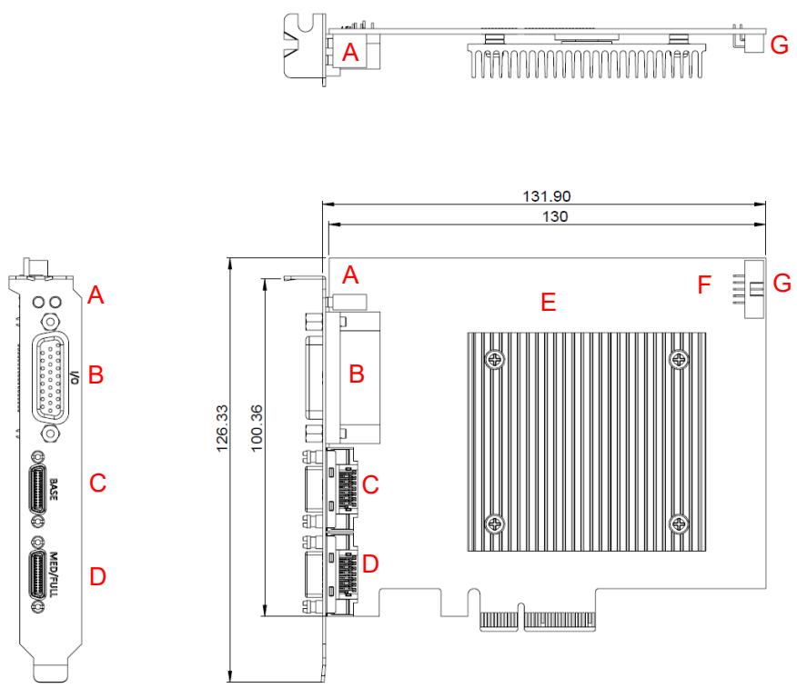
![A\nB\nC\nD\n126.33\n100.36\n131.90\n130\nA\nB\nC\nD\nE\nF\nG](.pcie-cpl64v-50m-18534-1000-10/1fa7a957a821d98f8cc3f9d982daa5eddb1165c453fc0afee11077c694dba1e7.jpg)

Figure 1: PCIe-CPL64V layout

<table><tr><td>Position</td><td>Function</td><td>Description</td></tr><tr><td>A</td><td>LED7</td><td>Camera link status LED</td></tr><tr><td>B</td><td>CN2</td><td>D-Sub I/O connector</td></tr><tr><td>C</td><td>CN5</td><td>Camera link base video input</td></tr><tr><td>D</td><td>CN6</td><td>Camera link medium / full video input</td></tr><tr><td>E</td><td>SW1</td><td>Card ID switch</td></tr><tr><td>F</td><td>LED2</td><td>Multi-card sync status LED</td></tr><tr><td>G</td><td>CN4</td><td>Multi-card sync connector</td></tr></table>

# 2.3 Connectors, I/O, Controls

# 2.3.1 Camera Link Video Inputs (CN5 & CN6)

![Base\nMedium/Full](.pcie-cpl64v-50m-18534-1000-10/c2cbf8fa57c4abb214d807de2846a2d489c0c43b9641cd307aa1de1546ac146f.jpg)

Figure 2: Camera link video inputs

# 2.3.1.1 Camera Link Base (CN5)

<table><tr><td>Pin</td><td>Function</td><td>Description</td><td>Pin</td><td>Function</td><td>Description</td></tr><tr><td>1</td><td>GND / PoCL_+12V</td><td>nonPoCL: Digital GND PoCL: PoCL Power</td><td>14</td><td>GND</td><td>Digital GND</td></tr><tr><td>2</td><td>CC4-</td><td>Control signal pair-</td><td>15</td><td>CC4+</td><td>Control signal pair+</td></tr><tr><td>3</td><td>CC3+</td><td>Control signal pair+</td><td>16</td><td>CC3-</td><td>Control signal pair-</td></tr><tr><td>4</td><td>CC2-</td><td>Control signal pair-</td><td>17</td><td>CC2+</td><td>Control signal pair+</td></tr><tr><td>5</td><td>CC1+</td><td>Control signal pair+</td><td>18</td><td>CC1-</td><td>Control signal pair-</td></tr><tr><td>6</td><td>STFG+</td><td>Serial com. Pair+</td><td>19</td><td>STFG-</td><td>Serial com. Pair-</td></tr><tr><td>7</td><td>STC-</td><td>Serial com. Pair-</td><td>20</td><td>STC+</td><td>Serial com. Pair+</td></tr><tr><td>8</td><td>X3+</td><td>Base data pair+</td><td>21</td><td>X3-</td><td>Base data pair-</td></tr><tr><td>9</td><td>XCLK+</td><td>Base clock pair+</td><td>22</td><td>XCLK-</td><td>Base clock pair-</td></tr><tr><td>10</td><td>X2+</td><td>Base data pair+</td><td>23</td><td>X2-</td><td>Base data pair-</td></tr><tr><td>11</td><td>X1+</td><td>Base data pair+</td><td>24</td><td>X1-</td><td>Base data pair-</td></tr><tr><td>12</td><td>X0+</td><td>Base data pair+</td><td>25</td><td>X0-</td><td>Base data pair-</td></tr><tr><td>13</td><td>GND</td><td>Digital GND</td><td>26</td><td>GND / PoCL_+12V</td><td>nonPoCL: Digital GND PoCL: PoCL Power</td></tr></table>

2.3.1.2 Camera Link Medium/Full (CN6)

<table><tr><td>Pin</td><td>Function</td><td>Description</td><td>Pin</td><td>Function</td><td>Description</td></tr><tr><td>1</td><td>GND / PoCL_+12V</td><td>nonPoCL: Digital GND PoCL: PoCL Power</td><td>14</td><td>GND</td><td>Digital GND</td></tr><tr><td>2</td><td>Z3+</td><td>Full data pair+</td><td>15</td><td>Z3-</td><td>Full data pair-</td></tr><tr><td>3</td><td>ZCLK+</td><td>Full clock pair+</td><td>16</td><td>ZCLK-</td><td>Full clock pair-</td></tr><tr><td>4</td><td>Z2+</td><td>Full data pair+</td><td>17</td><td>Z2-</td><td>Full data pair-</td></tr><tr><td>5</td><td>Z1+</td><td>Full data pair+</td><td>18</td><td>Z1-</td><td>Full data pair-</td></tr><tr><td>6</td><td>Z0+</td><td>Full data pair+</td><td>19</td><td>Z0-</td><td>Full data pair-</td></tr><tr><td>7</td><td>Terminated</td><td>100 Ω terminated</td><td>20</td><td>Terminated</td><td>100 Ω terminated</td></tr><tr><td>8</td><td>Y3+</td><td>Medium data pair+</td><td>21</td><td>Y3-</td><td>Medium data pair-</td></tr><tr><td>9</td><td>YCLK+</td><td>Medium clock pair+</td><td>22</td><td>YCLK-</td><td>Medium clock pair-</td></tr><tr><td>10</td><td>Y2+</td><td>Medium data pair+</td><td>23</td><td>Y2-</td><td>Medium data pair-</td></tr><tr><td>11</td><td>Y1+</td><td>Medium data pair+</td><td>24</td><td>Y1-</td><td>Medium data pair-</td></tr><tr><td>12</td><td>Y0+</td><td>Medium data pair+</td><td>25</td><td>Y0-</td><td>Medium data pair-</td></tr><tr><td>13</td><td>GND</td><td>Digital GND</td><td>26</td><td>GND / PoCL_+12V</td><td>nonPoCL: Digital GND PoCL: PoCL Power</td></tr></table>

# 2.3.2 D-SUB 26-Pin I/O Connector (CN2)

![Technical line drawing of a dual-port electronic device with two 16-pin connectors and terminal blocks (no text or symbols)](.pcie-cpl64v-50m-18534-1000-10/46f42a22628d22374a8c977352d1c9127540ab10634c6f3ee540101b86868db9.jpg)

Figure 3: D-SUB 26-pin I/O

<table><tr><td>Pin</td><td>Function</td><td>Description</td><td>Pin</td><td>Function</td><td>Description</td></tr><tr><td>1</td><td>NC</td><td>Floating</td><td>14</td><td>DI2+</td><td>Digital Input Pair2+</td></tr><tr><td>2</td><td>EB+</td><td>Encoder Input Pair B+</td><td>15</td><td>DI3+</td><td>Digital Input Pair3+</td></tr><tr><td>3</td><td>DI0+</td><td>Digital Input Pair0+</td><td>16</td><td>DO1+</td><td>Digital Output1</td></tr><tr><td>4</td><td>DI2-</td><td>Digital Input Pair2-</td><td>17</td><td>DO3+</td><td>Digital Output3</td></tr><tr><td>5</td><td>DI3-</td><td>Digital Input Pair3-</td><td>18</td><td>DO3-</td><td>DO GND</td></tr><tr><td>6</td><td>DO1-</td><td>DO GND</td><td>19</td><td>EA-</td><td>Encoder Input Pair A-</td></tr><tr><td>7</td><td>NC</td><td>Floating</td><td>20</td><td>EA+</td><td>Encoder Input Pair A+</td></tr><tr><td>8</td><td>NC</td><td>Floating</td><td>21</td><td>DI1-</td><td>Digital Input Pair1-</td></tr><tr><td>9</td><td>NC</td><td>Floating</td><td>22</td><td>DO0-</td><td>DO GND</td></tr><tr><td>10</td><td>NC</td><td>Floating</td><td>23</td><td>DO0+</td><td>Digital Output0</td></tr><tr><td>11</td><td>EB-</td><td>Encoder Input Pair B-</td><td>24</td><td>DO2-</td><td>DO GND</td></tr><tr><td>12</td><td>DI0-</td><td>Digital Input Pair0-</td><td>25</td><td>DO2+</td><td>Digital Output2</td></tr><tr><td>13</td><td>DI1+</td><td>Digital Input Pair1+</td><td>26</td><td>NC</td><td>Floating</td></tr></table>

# 2.3.3 Camera Link Status LED (LED7)

![Technical line drawing of a computer interface panel with connectors and ports (no text or symbols)](.pcie-cpl64v-50m-18534-1000-10/bd83356b345665c87a108054b315842c91975dfd6ed77d1c4f1e2311a79723f2.jpg)

Figure 4: Camera link status LED

![SEFUG\nUG\nPCB](.pcie-cpl64v-50m-18534-1000-10/9f89d58f52a1125522c1a3dea97302b97895a2fcc05d347eb1be52fbb80c858c.jpg)

<table><tr><td>Function</td><td>Status / Color</td></tr><tr><td>Camera LinkConfiguration(SEFUG)</td><td>- Full Camera Detected : Green ON- Medium Camera Detected : Green Blinking (2Hz)- Base Camera Detected : Orange ON- Abnormal status : Orange Blinking (2Hz)- Not detected : OFF</td></tr><tr><td>Capture Image(UG)</td><td>- Start Capture : Green ON- Capturing : Green Blinking (2Hz)- Stop Capture / Time out : OFF</td></tr></table>

# Note:

• The Camera Link configuration is referenced to the camera’s clock.
If only Pair X is detected, it is determined as Base.
If Pair X and Pair Y are detected, it is determined as Medium.
If Pair X, Pair Y, and Pair Z are detected, it is determined as Full.
• Any other pair combination is considered abnormal.
• If the camera outputs all three clock pairs simultaneously, it is determined as Full.

# 2.3.4 Multi-Card Sync. Connector (CN4)

![Simple line drawing of a door with handle and seat, no text or symbols present](.pcie-cpl64v-50m-18534-1000-10/94af1d44b32fb0c6fd5a75fc06fa3f722f68b225c17608db7ad96befe461c520.jpg)

![CN4\n1 2\n3 4\n5 6\n7 8\n9 10\nBH_10_R2.0mm](.pcie-cpl64v-50m-18534-1000-10/2c4beb450d3e3cc405544fef1b1f201afdf09cd910664c2082cec9f909a4a7d3.jpg)

<table><tr><td>Pin</td><td>Function</td><td>Description</td><td>Pin</td><td>Function</td><td>Description</td></tr><tr><td>1</td><td>GND</td><td>Digital GND</td><td>2</td><td>GND</td><td>Digital GND</td></tr><tr><td>3</td><td>CARD_SYNC1</td><td>Multi-card sync. Signal 1</td><td>4</td><td>GND</td><td>Digital GND</td></tr><tr><td>5</td><td>Reserve</td><td>Reserve</td><td>6</td><td>GND</td><td>Digital GND</td></tr><tr><td>7</td><td>Reserve</td><td>Reserve</td><td>8</td><td>GND</td><td>Digital GND</td></tr><tr><td>9</td><td>Reserve</td><td>Reserve</td><td>10</td><td>GND</td><td>Digital GND</td></tr></table>

Note: The master card and the slave card are connected via a dedicated cable.

# 2.3.5 Multi-Card Status LED (LED2)

![Multi-Card Sync.](.pcie-cpl64v-50m-18534-1000-10/a9d0f761ecf3c21612260fad92188a88e93dc7051634f61db43dc4bb122ef362.jpg)

<table><tr><td>Function</td><td>Status/ Color</td></tr><tr><td>Multi-card Sync. Info</td><td>- Master Mode : Red ON- Slave Mode : Green ON- Sync. Disable : OFF (Default)</td></tr></table>

# 2.3.6 Card ID Select (SW1)

![The image shows a diagram labeled 'ON' in the top left corner. Below it are four rectangular boxes arranged in a row. Each box has a white top half and a grey bottom half. Underneath each box is a number, reading '1', '2', '3', and '4' from left to right.](.pcie-cpl64v-50m-18534-1000-10/7facded0946e90213d1c40d3b4863243878ceacc326e5c3396384d86cec75a31.jpg)

<table><tr><td>No. of ID</td><td>1</td><td>2</td><td>3</td><td>4</td></tr><tr><td>0 (Default)</td><td>OFF</td><td>OFF</td><td>OFF</td><td>OFF</td></tr><tr><td>1</td><td>ON</td><td>OFF</td><td>OFF</td><td>OFF</td></tr><tr><td>2</td><td>OFF</td><td>ON</td><td>OFF</td><td>OFF</td></tr><tr><td>3</td><td>ON</td><td>ON</td><td>OFF</td><td>OFF</td></tr><tr><td>4</td><td>OFF</td><td>OFF</td><td>ON</td><td>OFF</td></tr><tr><td>5</td><td>ON</td><td>OFF</td><td>ON</td><td>OFF</td></tr><tr><td>6</td><td>OFF</td><td>ON</td><td>ON</td><td>OFF</td></tr><tr><td>7</td><td>ON</td><td>ON</td><td>ON</td><td>OFF</td></tr><tr><td>8</td><td>OFF</td><td>OFF</td><td>OFF</td><td>ON</td></tr><tr><td>9</td><td>ON</td><td>OFF</td><td>OFF</td><td>ON</td></tr><tr><td>10</td><td>OFF</td><td>ON</td><td>OFF</td><td>ON</td></tr><tr><td>11</td><td>ON</td><td>ON</td><td>OFF</td><td>ON</td></tr><tr><td>12</td><td>OFF</td><td>OFF</td><td>ON</td><td>ON</td></tr><tr><td>13</td><td>ON</td><td>OFF</td><td>ON</td><td>ON</td></tr><tr><td>14</td><td>OFF</td><td>ON</td><td>ON</td><td>ON</td></tr><tr><td>15</td><td>ON</td><td>ON</td><td>ON</td><td>ON</td></tr></table>

Note: When using multiple cards, each card must be assigned a different card ID.

# 2.4 I/O Interface

# 2.4.1 Encoder Differential Input (EA & EB)

The PCIe-CPL64V includes A-B encoder signals, the input signal for the encoder capture mode.

The phase A input is for the Channel 0 Line/Area Trigger input when set to the Line Area Trigger capture mode. The phase B input is for the Channel 0 Line/Area Trigger input when set to the Line Area Trigger capture mode.

![Isolation\nEA/B+\nEA/B-\nVDD\nData](.pcie-cpl64v-50m-18534-1000-10/ecd1ebbd8815796e63ab9326613be28b18cabaa72cd820572d2153baedf477f3.jpg)

Figure 5: Encoder differential input schematic

The PCIe-CPL64V provides Bipolar Isolation Input ports

<table><tr><td>Function</td><td>Specification</td></tr><tr><td>Max. Common-Mode Input Range</td><td>±7V</td></tr><tr><td>Max. Positive-going input threshold voltage</td><td>0.2V</td></tr><tr><td>Min. Negative-going input threshold voltage</td><td>-0.2V</td></tr></table>

# 2.4.2 2.4.2 Digital Input (DI0-DI3)

![DI0~3+\nIsolation\nMax. 24V\nDI0~3-\nVDD\ncontrol circuit](.pcie-cpl64v-50m-18534-1000-10/808cf2381f08cc39beac5e1cf7c2a6736002d4a4fdbd75c89d04029d1783b724.jpg)

Figure 6: Digital input schematic

The PCIe-CPL64V provides bipolar isolation input ports.

<table><tr><td>Function</td><td>Specification</td></tr><tr><td>Input voltage range</td><td>0 to 24V</td></tr><tr><td>Input Low level</td><td>0 to 0.8V</td></tr><tr><td>Input High level</td><td>3 to 24V</td></tr></table>

# 2.4.3 2.4.2 Digital Output (DO0-DO3)

![control circuit\nDO0~3 Isolation\nMax. 80mA\nload\nDC Max. 30V\nDO GND](.pcie-cpl64v-50m-18534-1000-10/d02bfdf8ab86911c794e787b604a96ae5616ec8ec625aa9053c5a27b6717aeef.jpg)

Figure 7: Digital output schematic

The PCIe-CPL64V provides open-drain isolation output ports.

<table><tr><td>Function</td><td>Specification</td></tr><tr><td>Output voltage range</td><td>Open-drain max. to 30V</td></tr><tr><td>Output Low level</td><td>0 to 0.8V</td></tr></table>

# 3 Getting Started

# 3.1 Unpacking Checklist

Before unpacking, check the shipping carton for any damage. If the shipping carton and/or contents are damaged, inform your dealer immediately. Retain the shipping carton and packing materials for inspection. Obtain authorization from your dealer before returning any product to ADLINK. Ensure that the following items are included in the package.

• PCIe-CPL64V unit

Note: ODM versions with non-standard configuration, functionality, or packaging may vary according to individual requirements.

# 3.2 Hardware Installation

1. Remove the computer cover according to the computer manual.
2. Remove the slot cover (if any).
3. Carefully position the board in the selected PCI Express If installing in a tower computer, align the board with the board slots.
4. Press the board firmly but carefully into the connector.
5. Anchor the board with the screw.
6. Connect the Camera Link device via SDR connector.
7. Power up the computer.
8. Locate the system controller slot (Slot 1).

# Note:

• The Camera Link configuration is referenced to the camera’s clock.
• If only Pair X is detected, it is determined as Base.
If Pair X and Pair Y are detected, it is determined as Medium.

# 3.3 Driver Installation

# 3.3.1 System Requirement

Windows requires one of the following operating systems to be installed on your computer: Win10 x64 or Win11 x64
• To create a new project for any .NET language. The project needs to target .NET Framework 4.0 or a later version (4.8).
• Visual C++ Redistributable Package 2015 or a later version. C++ MFC is optional based on your project version.
• Power saving modes of the operating systems are not supported.
• Kernel DMA Protection is not supported.

# 3.3.2 PCIe-CPL64V Driver Installation

Follow the instructions in the setup wizard. The wizard will guide you through the installation process.

1. Click to run the AVS SDK installation file
2. Click the “Next” button then the SDK and driver will begin installing. Remove the slot cover (if any).

![ADLINK Vision Software SDK - InstallShield Wizard\nWelcome to the InstallShield Wizard for\nADLINK Vision Software SDK\nThe InstallShield(R) Wizard will install ADLINK Vision Software\nSDK on your computer. To continue, click Next.\nWARNING: This program is protected by copyright law and\ninternational treaties.\n( Back	Next )	Cancel](.pcie-cpl64v-50m-18534-1000-10/c812e4730798e291a8aeaad92115022939bbd87dcf28eac58a45117eaf2797a0.jpg)

3. Please read the license agreement and select “I accept…” Click “Next”

![ADLINK Vision Software SDK - InstallShield Wizard\nLicense Agreement\nPlease read the following license agreement carefully.\nLICENSE AGREEMENT\nIMPORTANT: PLEASE READ THE TERMS AND CONDITIONS OF\nTHIS LICENSE AGREEMENT ('LICENSE AGREEMENT')\nCAREFULLY BEFORE USING THE PRODUCT(PRODUCT)\nPROVIDED BY ADLINK TECHNOLOGY INC ('ADLINK').\nADLINK, IS WILLING TO SELLING THE PRODUCT TO\nCUSTOMER AS THE INDIVIDUAL, THE COMPANY, OR THE\nLEGAL ENTITY THAT WILL BE UTILIZING. ASSAMBLING OR\nI accept the terms in the license agreement\nPrint\nI do not accept the terms in the license agreement\nInstallShield\n( Back	Next )	Cancel](.pcie-cpl64v-50m-18534-1000-10/1daf3172aa0a21843aa86b3058ffd133f712f12e32cf4ca8b91b5436ebf2775a.jpg)

ADLINK Vision Software SDK - InstalIShield Wizard

![Abstract blue gradient background with a small white icon and triangular shapes (no text or symbols)](.pcie-cpl64v-50m-18534-1000-10/13e42e421a9e2ed1ae74c9fabde27ba29dc418aeae5529a6cc23d9c05554d737.jpg)

# Preparing to Insta..

ADLINK Vision Software SDK Setup is preparing the InstallShield Wizard, which will guide you through the program setup process. Please wait.

Extracting: ADLINK Vision Software SDK.msi

Cancel

4. Select the destination folder for installing. (Default path is C:\Program Files\ADLINK\AVS). Click “Install”

![ADLINK Vision Software SDK - InstallShield Wizard\nDestination Folder\nClick Next to install to this folder, or click Change to install to a different folder.\nInstall ADLINK Vision Software SDK to:\nC:\Program Files\ADLINK\AVS\\nChange...\nInstallShield\n( Back	Next )	Cancel](.pcie-cpl64v-50m-18534-1000-10/dba84807c4df74a6760589841ed872f00db122347cc185dd5f765bf92edafa32.jpg)

![ADLINK Vision Software SDK - InstallShield Wizard\nReady to Install the Program\nThe wizard is ready to begin installation.\nClick Install to begin the installation.\nIf you want to review or change any of your installation settings, click Back. Click Cancel to exit the wizard.\nInstallShield\n( Back	Install	Cancel](.pcie-cpl64v-50m-18534-1000-10/d1f0a0a73219b005300dd7a073008c4cfac3954cf513f4745b38e52732014d08.jpg)

![ADLINK Vision Software SDK - InstallShield Wizard\nInstalling ADLINK Vision Software SDK\nThe program features you selected are being installed.\nPlease wait while the InstallShield Wizard installs ADLINK Vision Software SDK. This may take several minutes.\nStatus:\nCopying new files\nInstallShield\n( Back	Next )	Cancel](.pcie-cpl64v-50m-18534-1000-10/9a77d653a809f4337d59e7afeecfdb02380aee93223fbfca274ef475bd7c983a.jpg)

5. When the installation is successful, a window is displayed. Click “Finish”

![ADLINK Vision Software SDK - InstallShield Wizard\nInstallShield Wizard Completed\nThe InstallShield Wizard has successfully installed ADLINK Vision Software SDK. Click Finish to exit the wizard.\n( Back	Finish	Cancel](.pcie-cpl64v-50m-18534-1000-10/7166f0f3b1bd3d90e481ce5fd3eee90eff60dba921696b6c47b2a116efb01476.jpg)

6. Click “Yes” and restart the system.

![ADLINK Vision Software SDK Installer Information\nYou must restart your system for the configuration changes made to ADLINK Vision Software SDK to take effect. Click Yes to restart now or No if you plan to restart later.\nYes	No](.pcie-cpl64v-50m-18534-1000-10/bfcee96286b50f922e273bed8a1e059b1471676fa88e82e08f3a7846a4156d68.jpg)

Note: The PCIe-CPL64V series products cannot be mixed with or used alongside the legacy PCIe-CPL64 series products. Please ensure that the SDK and drivers for the PCIe-CPL64 series are completely removed before using the PCIe-CPL64V series products.

7. Go to the system control panel and check the following:

ADLINK PCIe-CPL64V Full
• ADLINK PCIe-CPL64V Full Port (COMXX)

When operating in a two-card configuration, the System Control Panel should be displayed as shown in the figure below.

![adlink\nAudio inputs and outputs\nComputer\nDisk drives\nDisplay adaptors\nFirmware\nHuman Interface Devices\nIDE ATA/ATAPI controllers\nKeyboards\nMice and other pointing devices\nMonitors\nMultifunction adapters\nADLINK PCIe-CPL64V Full\nADLINK PCIe-CPL64V Full\nNetwork adapters\nPorts (COM & LPT)\nADLINK PCIe-CPL64V Full Port 0 (COM27)\nADLINK PCIe-CPL64V Full Port 0 (COM28)\nCommunications Port (COM1)\nUSB Serial Port (COM5)\nPrint queues\nProcessors\nSoftware components\nSoftware devices\nSound, video and game controllers](.pcie-cpl64v-50m-18534-1000-10/da8a4eb8d918992d784976850c8c06c2324ce9e9194183ada17db7f428e48af9.jpg)

Note: If you encounter a COM port conflict, please manually remove the residual COM ports

![User Account Control Settings\nChoose when to be notified about changes to your computer\nUser Account Control helps prevent potentially harmful programs from making changes to your computer.\nTell me more about User Account Control settings\nAlways notify\nNever notify me when:\n• Applications try to install software or make changes to my computer\n• I make changes to Windows settings\ni Not recommended.\nNever notify\nOK Cancel](.pcie-cpl64v-50m-18534-1000-10/38c6682f2c77b36d77890e6a26f8bd00e66f7bdab77896e12b934303878532d0.jpg)

Note: When using Windows 10/11, the User Account Control (UAC) feature must be disabled before using the PCIe-CPL64V. Open the Control Panel by searching for it in the Start Menu. Then, navigate to the "User Accounts" section. Here, you will find the option to "Change User Account Control settings." Click on it. In the UAC settings window, you will see a slider with different levels of security. To disable UAC, simply move the slider all the way down to the "Never notify" option. Click "OK" to save the changes for the PCIe-CPL64V to function normally under Windows 10/11.

# 4 Trigger Architecture

# 4.1 Trigger Block Diagram

![**Blocks:**\n*   Trigger Source Selection\n*   Trigger Delay Setting\n*   Re-trigger Setting\n*   Digital Output and Camera Control Setting\n*   Multi-Card Sync. Output\n\n**Connections:**\n*   A blue arrow points from **Trigger Source Selection** to **Trigger Delay Setting**.\n*   A blue arrow points from **Trigger Delay Setting** to **Re-trigger Setting**.\n*   A blue arrow points from **Re-trigger Setting** to **Digital Output and Camera Control Setting**.\n*   A separate blue arrow originates from the bottom of **Trigger Source Selection**, extends downward, turns right, and points into **Multi-Card Sync. Output**.](.pcie-cpl64v-50m-18534-1000-10/bae328267c4646181e33677a25e56808eeff14337847c2aaff34c97961d4b8a7.jpg)

Trigger settings can be configured based on user requirements.

The following sections describe the Trigger Block Diagram and related settings.

# Trigger Source Selection

The trigger source for Digital Output and Camera Control can be selected from Encoder, Digital Input, Software Trigger, or Multi-card Sync. Input.

# Trigger Delay Setting

Digital Output and Camera Control support delayed trigger output, which can be configured in either Encoder mode or Timer mode.

# Re-trigger Setting

Set the number of re-trigger and the trigger conditions.

A fixed Encoder or Timer can be specified as the condition for repeated triggering, which is commonly used in Line Scan mode.

# Digital Output and Camera Control Setting

Configure the output mode for Digital Output and Camera Control, which can be set to either manual mode or trigger mode. In trigger mode, the pulse width for high and low levels must be specified.

# Multi-card Sync. Output

Multi-card synchronous triggering can be achieved through the CN4 connector.

# 4.1.1 Trigger Source and Selection

Trigger Source Selection
![The diagram illustrates a multiplexing process with the following labeled blocks and connections:\n\n**Input Blocks (Left Column):**\nSeven blocks on the left have arrows pointing to the central block:\n*   Encoder CompareCount\n*   Digital Input0\n*   Digital Input1\n*   Digital Input2\n*   Digital Input3\n*   SW Trigger\n*   Multi-Card Sync. Input\n\n**Central Block:**\n*   MUX\n\n**Output Blocks (Right Side):**\nThe MUX block has arrows connecting to two blocks on the right:\n1.  A large block containing the text:\n    *   (TriggerOutputSrc)\n    *   DO0 TriggerSource\n    *   /\n    *   DO1 TriggerSource\n    *   /\n    *   DO2 TriggerSource\n    *   /\n    *   DO3 TriggerSource\n    *   /\n    *   Port0CC1 TriggerSource\n    *   /\n    *   Port0CC2 TriggerSource\n2.  A smaller block below containing the text:\n    *   (Multi-Card Sync. TrgScr)\n    *   Trigger Source](.pcie-cpl64v-50m-18534-1000-10/ebfd7eeb19137ec46efbb62666c60fb9b67b32e377fbc8d58581d5db23ccc98f.jpg)

Users should select the input trigger source for every output channel that is enabled. There are 7 different types of trigger source including DI0-DI3 Event, encoder compare event, Multi-card sync trigger event, and software trigger event.

For DI0-DI3, polarity can be changed to rising or falling, we also provide a debounce filter with several different debounce time. The DI0-3 Event will be generated accordingly if the corresponding signal level is detected.

For encoder compare event, the trigger will be generated if the encoder value equals the compare value.

For Multi-card sync event, we use this trigger source to do Multi-card synchronization. User needs to select a card to be master and others to be slave. Only slaves listen to this event. The master is responsible for generating the Multi-card sync event for all the slaves.

For software trigger event, this is just a manual trigger event by software.

Note: Users should set the TriggerSource parameter for every Output channel, including 4 DO channels and 2 CC Lines.

# 4.1.2 Trigger Delay Setting

Trigger Delay Setting
![The image displays a simple flowchart consisting of two blocks arranged horizontally.\n\n*   **Block 1:** A rounded rectangle on the left containing the text **'Delay Mode'**.\n*   **Connection:** A blue arrow points to the right, originating from the first block and pointing towards the second block.\n*   **Block 2:** A rounded rectangle on the right containing the text **'Delay Count'**.](.pcie-cpl64v-50m-18534-1000-10/3789b4c3b235d9d7273d8ff233625291105222f48de9f8d6231cec356b2398ca.jpg)

This part is for trigger delay that users can set by timer or by encoder.

There are two parameters in this block:

Delay Mode: can be set to timer (in 1µs unit) or encoder
Delay Count: the value to be delayed

Example: when delay count is set to 1000: If the delay mode is set to timer mode, this block will delay the trigger for 1000 µs. If the delay mode is set to encoder, the trigger will be delayed until the encoder value is reached, which is the current encoder value plus 1000.

# 4.1.3 Re-trigger Setting

![The diagram is titled 'Re-trigger Setting' and is enclosed within a dashed border. It features the following labeled blocks and connections:\n\n1.  **Retrigger Enable**: Located at the top left.\n    *   A long horizontal arrow labeled **Disable (Bypass)** points to the right from this block.\n    *   A vertical arrow labeled **Enable** points downward to the **Mode** block.\n2.  **Mode**: Located at the bottom left.\n    *   A horizontal arrow points right to the **Interval** block.\n3.  **Interval**: Located at the bottom center.\n    *   A horizontal arrow points right to the **TriggerNums** block.\n4.  **TriggerNums**: Located at the bottom right.](.pcie-cpl64v-50m-18534-1000-10/358222f2a4ec4ef261e9ac7961601e1b7f36a7282378c8100e6910105d32a75b.jpg)

Once a trigger is received, Retrigger Block will generate a number of triggers by a pre-defined interval if the retrigger enable parameter is set. This function is usually suitable for applications related to line scan cameras.

Example: generating 10 CC1 signals for the camera per every 20 encoder counts when triggered: Then, we should enable CC1RetriggerEnable, set the CC1Mode to encoder mode, set the CC1interval to 20 and the CC1TriggerNums to 10.

# 4.1.4 Trigger Output and Camera Control (CC1, CC2)

Digital Output and Camera Control Setting
![The flowchart begins with a top-left block labeled **Output Mode**. From this block, two paths diverge:\n\n1.  **Manual path:** An arrow labeled **Manual mode** points to the right, connecting to a block labeled **Status**.\n2.  **Trigger path:** A downward arrow labeled **Trigger mode** connects to a second block at the bottom left also labeled **Output Mode**.\n\nFrom the bottom-left **Output Mode** block, the flow continues horizontally to the right:\n*   An arrow connects to a block labeled **HighPulseWidth**.\n*   A subsequent arrow connects **HighPulseWidth** to a final block labeled **LowPulseWidth**.](.pcie-cpl64v-50m-18534-1000-10/f0fb82b46af65bd0ca052157819c2fcf163493e10633c3c4793844259f7fc22d.jpg)

This block is responsible for generating the output PWM pulse or output level. We support 2 modes in this block. In manual mode, users can control the output pin manually by software. In trigger mode, the pre-defined PWM signal will be generated if the trigger event is received.

To select the mode, we use DOxOutputMode or CCxOutputMode. The PWM pulse width can also be set for the low part and the high part duration.

# 4.1.5 Multi-Card Sync.

![The diagram displays a workflow divided into two main horizontal sections representing a 'Master Card' and a 'Slave Card' system.\n\n**Top Section (Master Card):**\n*   **Left Box:** A dashed box labeled **'Trigger Source Selection'** contains a block labeled **'MUX'**, which receives three blue input arrows (one solid, one dotted, one solid). An arrow connects 'MUX' to a block labeled **'(Multi-Card Sync. TrgScr) Trigger Source'**.\n*   **Right Box:** A dashed box labeled **'Multi-Card Sync. Output'** (with the label **'( Master Card )'** next to it) contains a block labeled **'Mode'**.\n*   **Connections:** An arrow connects '(Multi-Card Sync. TrgScr) Trigger Source' to the 'Mode' block. An arrow labeled **'Master'** exits the 'Mode' block to the right.\n\n**Connecting Element:**\n*   A thick blue curved arrow labeled **'Multi-card Sync. cable'** connects the 'Master' output from the top section down to the bottom section.\n\n**Bottom Section (Slave Card):**\n*   **Right Box:** A dashed box labeled **'Multi-Card Sync. Output'** (with the label **'( Slave Card )'** next to it) contains a block labeled **'Mode'**.\n*   **Left Box:** A dashed box labeled **'Trigger Source Selection'** contains a block labeled **'Multi-Card Sync. Input'**.\n*   **Connections:** The thick blue 'Multi-card Sync. cable' arrow points into the '( Slave Card )' area. An arrow labeled **'Slave'** exits the 'Mode' block and points left into the 'Multi-Card Sync. Input' block.](.pcie-cpl64v-50m-18534-1000-10/8f8210c367b2b0dded44c1aefb4fb68631de41967fb06891c1cc1e13a0c18b1a.jpg)

The PCIe-CPL64V provides a multi-card synchronization mechanism for users.

Users must select one card as the master card, while the remaining cards serve as slave cards. Communication among the cards is achieved through the Multi-card Sync. Connector and cable.

The master card is responsible for generating multi-card synchronization events, which are monitored by all slave cards.

For the configuration of Trigger Source, please refer to Section 4.1.1.

# 5 CAM File

# 5.1 CAM File Introduction

ADLINK PCIe-CPL64V Frame Grabbers support .ini files for camera configuration.

Camera Configuration File (referred to as CAM file hereafter) templates serve as cameraspecific parameter sets that configure the grabber channel via AVS Camera Link feature parameter
 The frame grabber driver processes a Cam file by executing a sequence of write parameter calls—essentially mapping camera settings into the AVS API.
 Standard templates are installed under …{Installfolder}\ADLINK\AVS\CameraFile

Warning: When the frame grabber starts capturing images, dynamic parameter settings are not supported.

# 5.1.1 Importing CAM File

Cam files are intended to be customized by PCIe-CPL64V users who want to interface a particular camera with a PCIe-CPL64V board. They allow users to set certain section settings, for example, only import the [ImageFormat] and [TriggerOutput]…etc.

# 5.1.2 Image Format Section

```ini
[ImageFormat]
SensorWidth = 32 to 65504
SensorHeight = 0 to 65535
Tap = 1 / 10 / 2 / 4 / 8
PixelSize = 10 / 12 / 8
TapPlacement = 1x / 1x10 / 1x2 / 1x4 / 1x8
PixelFormat = Mono / RGB
FVALEnable = False / True
LVALEnable = False / True
DVALEnable = False / True
FVALPolarity = Falling / Rising
LVALPolarity = Falling / Rising
DVALPolarity = Falling / Rising
```

 Supported image pixel formats are set by the combination of {PixelFormat/PixelSize}. The available formats are RGB8, RGB12, Mono8, Mono10 , Mono12.

<table><tr><td>Tap Configuration</td><td>1tap</td><td>2tap</td><td>4tap</td><td>8tap</td><td>10tap</td></tr><tr><td>Mono8</td><td>V</td><td>V</td><td>V</td><td>V</td><td>V</td></tr><tr><td>Mono10</td><td>V</td><td>V</td><td>V</td><td>V</td><td></td></tr><tr><td>Mono12</td><td>V</td><td>V</td><td>V</td><td></td><td></td></tr><tr><td>RGB8</td><td>V</td><td>V</td><td></td><td></td><td></td></tr><tr><td>RGB12</td><td>V</td><td></td><td></td><td></td><td></td></tr></table>

Note: ODM versions with non-standard configuration, functionality, or packaging may vary according to individual requirements.

 TapPlacement needs to be matched with the Tap number. The available formats are {Tap/ TapPlacement} 1/1x, 2/1x2, 4/1x4, 8/1x8, 10/1x10.

EX: 1x1 designates that the pixels are delivered one at a time on a single tap beginning with the leftmost pixel of the top line.

![Based on the provided image, here is the description of the flowchart/block diagram:\n\n**Labeled Blocks:**\n*   **Top Block:** A horizontal rectangular structure divided into a left and right section. The left section consists of three cells with solid blue arrows pointing to the right. The right section consists of three cells with solid blue arrows pointing to the right. A dotted line connects the end of the left section to the start of the right section.\n*   **Bottom Block:** A horizontal rectangular structure divided into a left and right section. The left section consists of three cells with solid blue arrows pointing to the right. The right section consists of three cells with solid blue arrows pointing to the right. A dotted line connects the end of the left section to the start of the right section.\n\n**Connections:**\n*   **Connection labeled '1':** A diagonal dotted arrow line originating from the bottom-right corner of the Top Block and pointing to the bottom-left corner of the Bottom Block. The text '1' is located next to the center of this line.](.pcie-cpl64v-50m-18534-1000-10/1b1f45fd9e589e7f204ccc505da1dd007ab44c70da0c3b2549aa86a066e158f6.jpg)

EX: 1X4 designates four adjacent pixels that are delivered simultaneously on 4 taps beginning with the leftmost pixels.

![The diagram displays two horizontal rows of rectangular blocks arranged in a sequence.\n\n**Labeled Blocks:**\n*   **Top Row:** A sequence of blocks labeled 'Tap1', 'Tap2', 'Tap3', 'Tap4', followed by a gap labeled '...', and then another sequence of 'Tap1', 'Tap2', 'Tap3', 'Tap4'.\n*   **Bottom Row:** A sequence of blocks labeled 'Tap1', 'Tap2', 'Tap3', 'Tap4', followed by a gap labeled '...', and then another sequence of 'Tap1', 'Tap2', 'Tap3', 'Tap4'.\n*   The blocks are color-coded: 'Tap1' is light blue, 'Tap2' is light yellow, 'Tap3' is light green, and 'Tap4' is light orange.\n\n**Connections:**\n*   **Horizontal Arrows:** Inside each row, colored arrows point to the right.\n    *   A blue arrow spans 'Tap1' and 'Tap2'.\n    *   A yellow arrow spans 'Tap2' and 'Tap3'.\n    *   A green arrow spans 'Tap3' and 'Tap4'.\n    *   A brown arrow spans 'Tap4' and the subsequent 'Tap1'.\n    *   This pattern repeats across the row.\n*   **Diagonal Dotted Lines:** Four diagonal dotted lines connect the top row to the bottom row, labeled '1', '2', '3', and '4'. They have arrowheads pointing to the left.\n    *   Line '1' (blue) connects the end of the blue arrow in the top row (end of 'Tap2') to the start of the blue arrow in the bottom row (start of 'Tap1').\n    *   Line '2' (yellow) connects the end of the yellow arrow in the top row (end of 'Tap3') to the start of the yellow arrow in the bottom row (start of 'Tap2').\n    *   Line '3' (green) connects the end of the green arrow in the top row (end of 'Tap4') to the start of the green arrow in the bottom row (start of 'Tap3').\n    *   Line '4' (brown) connects the end of the brown arrow in the top row (end of the subsequent 'Tap1') to the start of the brown arrow in the bottom row (start of 'Tap4').](.pcie-cpl64v-50m-18534-1000-10/95bdca6b5862a87f7046775eb3d3bf5e917ab0d80bb76aceb7c9b89efe145a88.jpg)

When setting the image pixel formats and Tap number, the {CameraConfiguration} should be noted for setting Base, Medium, and/or Full.

<table><tr><td>Configuration</td><td>Number of Data Bits</td><td>Maximum Possible Throughput (MB/s)</td><td>Number of Cables Required</td></tr><tr><td>Base</td><td>24</td><td>255</td><td>1</td></tr><tr><td>Medium</td><td>48</td><td>510</td><td>2</td></tr><tr><td>Full</td><td>64</td><td>680</td><td>2</td></tr><tr><td>Full (80 bits)</td><td>80</td><td>850</td><td>2</td></tr></table>

PCIe-CPL64V boards unpack RGB 12-bit pixel component data into 16-bit pixel data for each RGB channel. Mono 10-bit and 12-bit pixel component data are also unpacked into 16-bit pixel data.
 The following tables show the data bits allocation.

<table><tr><td>{PixelFormat/PixelSize}</td><td>{Mono/8}</td><td>{Mono/10}</td><td>{Mono/12}</td></tr><tr><td>Unpacked data bits</td><td>8</td><td>16</td><td>16</td></tr></table>

<table><tr><td>{PixelFormat/PixelSize}</td><td>{RGB/8}</td><td>{ RGB/12}</td></tr><tr><td>Unpacked data bits</td><td>32</td><td>64</td></tr></table>

The significant bits of the pixel component data are aligned to the LSB of the data container. Padding dummy '0' bits are put as necessary in the most significant bits to reach the next 8- bit boundary. Example: RGB8 aligns to 2^n, allocating 4-byte data
? Mono8

![Byte 0\nBit7 Bit6 Bit5 Bit4 Bit3 Bit2 Bit1 Bit0\nM M M M M M M M\nPixel data for Mono](.pcie-cpl64v-50m-18534-1000-10/cf7e1fba97825980ad43009d1b5aa97e664340436b4f2a41e7a1f9b11b7caad1.jpg)

 Mono10

![Byte 1\nBit7 Bit6 Bit5 Bit4 Bit3 Bit2 Bit1 Bit0\n0 0 0 0 0 0 M M\nDummy\nByte 0\nBit7 Bit6 Bit5 Bit4 Bit3 Bit2 Bit1 Bit0\nM M M M M M M M M\nPixel data for Mono](.pcie-cpl64v-50m-18534-1000-10/90aee6052e2f05f70ababeee1bc7bdfb439df3354f074e8855ff3a25df92d39c.jpg)

 Mono12

![Byte 1\nBit7 Bit6 Bit5 Bit4 Bit3 Bit2 Bit1 Bit0\n0 0 0 0 M M M M\nDummy\nPixel data for Mono\nByte 0\nBit7 Bit6 Bit5 Bit4 Bit3 Bit2 Bit1 Bit0\nM M M M M M M\nM M M M M M M](.pcie-cpl64v-50m-18534-1000-10/0db2514f7b3b184b3be3d8ced17dcbc89addfcf39220d1334f0c9ef1b29379c6.jpg)

#  RGB8

![Byte 3\nBit7..0\n0 0 0 0 0 0 0 0 0\nDummy\nByte 2\nBit7..0\nB B B B B B B B B\nPixel data for Blue\nByte 1\nBit7..0\nG G G G G G G G G\nPixel data for Green\nByte 0\nBit7..0\nR R R R R R R R\nPixel data for Red](.pcie-cpl64v-50m-18534-1000-10/2364ab8cf94e56621005dce405864816120bb7aa83e3168c16b3f3da7df01594.jpg)

#  RGB12

Assume that you have chosen a 12-bit unpacked pixel format. The camera outputs 16 bits per pixel: 12 bits of pixel data and 4 padding bits to reach the next 8-bit boundary.

![Byte 7\nBit7..0\n00000000 00000000\nDummy\nByte 6\nBit7..0\n00000000\nDummy\nByte 5\nBit7..4\n0000\nBBBB\nPixel data for Blue\nByte 4\nBit3..0\nBBBBBBB\nBBBBBBB\nByte 3\nBit7..4\n0000\nDummy\nPixel data for Blue\nByte 2\nBit3..0\nGGGG\nPixel data for Green\nByte 1\nBit7..4\n0000\nDummy\nPixel data for Red\nByte 0\nBit3..0\nRRRR\nRRRRRRRR\nPixel data for Red](.pcie-cpl64v-50m-18534-1000-10/bdd4ac57affe36a6e43a913be24a887505a18834096996e73333fcbac4a92083.jpg)

Note: Image buffer declaration limitation: The total frame size must be a multiple of 32 bytes, and the width must be greater than or equal to 32 pixels.

The width multiple requirements are as follows:

For MONO 8-bit x 10tap: The Width should be a multiple of 160 pixels

For MONO 10-bit x 8tap: The Width should be a multiple of 320 pixels

For MONO 8-bit x 1tap/2tap/4tap/8tap: The Width should be a multiple of 32 pixels

For MONO 10-bit x 1tap/2tap/4tap: The Width should be a multiple of 16 pixels

For MONO 12-bit x 1tap/2tap/4tap: The Width should be a multiple of 16 pixels

For RGB 8-bit x 1tap/2tap: The Width should be a multiple of 8 pixels

For RGB 12-bit x 1tap: The Width should be a multiple of 4 pixels

Warning: If you set an incorrect image buffer size or tap placement, you will get an error when calling the AVS\_CameraLinkImportCamFile and AVS\_FrameGrabberStartAcquisition API.

The Camera Link standard requires that enabled signals are provided on Channel Link chips as follows:

<table><tr><td>Camera Link Configuration</td><td>FVAL</td><td>LVAL</td><td>DVAL</td></tr><tr><td>Base</td><td>X</td><td>X</td><td>X</td></tr><tr><td>Medium</td><td>X and Y</td><td>X and Y</td><td>X and Y</td></tr><tr><td>Full</td><td>X, Y and Z</td><td>X, Y and Z</td><td>X, Y and Z</td></tr><tr><td>80-bit</td><td>X only</td><td>X, Y and Z</td><td>-</td></tr></table>

Note: X: Cameralink chip X signals
Y: Cameralink chip Y signals
Z: Cameralink chip Z signals

The CAM files can be configured to enable/disable signals, such as Line Valid / Frame Valid / Data Valid.

Take 640 x 480 MONO 8-bit, 2-tap as an example:

![| Timing Type       | Tap1 | Tap2 |\n| ----------------- | ---- | ---- |\n| Vertical timing   | H x 480 | -    |\n| Horizontal Timing | Pixel clock x 320 | - |](.pcie-cpl64v-50m-18534-1000-10/b4bec6622ee1064dbeae1694311ff304da9a0e9bfb758ff0b99f1aa4e30f6f54.jpg)

Note: In 2-tap mode, each pixel clock can carry two-pixel data values.

# 5.1.3 Capture Mode Section

[CaptureMode]

ScanMode = AreaScan /LineScan

Please select the ScanMode based on your camera.
 Line Scan is ideal for high-speed processes and for inspecting continuous webs, surfaces, or large objects.
Area Scan is better suited for capturing detailed still images and for inspecting smaller, defined items.
 If the scan mode settings does not match the camera, the image will be erroneous or cannot be captured.

# 5.1.4 Trigger Input Section

[TriggerInput]
```ini
DI0TrigPolarity = Falling / Rising
DI1TrigPolarity = Falling / Rising
DI2TrigPolarity = Falling / Rising
DI3TrigPolarity = Falling / Rising
EnATrigPolarity = Falling / Rising
EnBTrigPolarity = Falling / Rising
DebounceTime = 0 / 200 / 500 / 800
```

 This section defines the trigger input polarity and debounce configuration for digital inputs and encoder triggers. These parameters determine how external trigger signals are interpreted by the system.

Note: The DebounceTime unit is nanosecond.

Warning: The trigger-related function are available only when AVS\_FrameGrabberStartAcquisition is called.

# 5.1.5 Trigger Output TrigSrc Section

Please refer to the introduction in Section 4.1.1 for instructions

[TriggerOutputTrigSrc]
```txt
DO0TriggerSource = DI0 / DI1 / DI2 / DI3 / Disable / EncoderComparator / MultiCardSync / SoftwareTrigger
DO1TriggerSource = DI0 / DI1 / DI2 / DI3 / Disable / EncoderComparator / MultiCardSync / SoftwareTrigger
DO2TriggerSource = DI0 / DI1 / DI2 / DI3 / Disable / EncoderComparator / MultiCardSync / SoftwareTrigger
DO3TriggerSource = DI0 / DI1 / DI2 / DI3 / Disable / EncoderComparator / MultiCardSync / SoftwareTrigger
Port0CC1TriggerSource = DI0 / DI1 / DI2 / DI3 / Disable / EncoderComparator / MultiCardSync / SoftwareTrigger
Port0CC2TriggerSource = DI0 / DI1 / DI2 / DI3 / Disable / EncoderComparator / MultiCardSync / SoftwareTrigger
```

PCIe-CPL64V provides 4 DO and CC1/CC2 outputs. Each output source supports multiple selections from one input signal source. DO outputs can be connected to different external devices, such as flashes based on the application. CC1 is used to send external triggers for camera.

Note: When MultiCardSync is set as the input signal source, MultiCardSync Mode in Section 5.1.8 needs to be set to Slave.

Note: SoftwareTrigger requires calling TriggerControl.SWTrigger via the Advanced Configuration API.

# 5.1.6 Encoder Input Section

This section configures the encoder interface behavior. The encoder inputs allow position or speed tracking based on signal transitions from external encoders.

[EncoderInput]
```txt
Mode = ABphaseX1 / ABphaseX2 / ABphaseX4 / CW/CCW / OUT/DIR
CompareCount = 0 ~ 4,294,967,295
```

Note: CompareCount sets the target count for comparison. Range: 0 to 4,294,967,295 (32-bit unsigned integer). This value can be used to trigger events when the encoder count reaches a specific value. |

# 5.1.7 Multi Card TrigSrc Section

[MultiCardTrigSrc]
```txt
TriggerSource = DI0 / DI1 / DI2 / DI3 / Disable / EncoderComparer / MultiCardSync / SoftwareTrigger
```

Note:To use the MultiCard synchronization function, you must select which TriggerSource serves as the initial signal source of the Master card. Please refer to Section 4.1.1

# 5.1.8 Multi-Card Sync Section

[MultiCardSync]
```txt
Mode = Master / Slave
```

Warning: When it is used as an output signal, it means that the card is the Master card and MultiCardSync Mode needs to be set to Master. When it is used as an input signal, it means that this card is the Slave card. In the same system, only one master card is allowed to exist. Please refer to Section 4.1.5 Multi-card Sync.

# 5.1.9 Trigger Delay Section

This section configures the trigger delay module behavior. The delay mode can be set based on EncoderMode or TimerMode. Please refer to the introduction in Section 4.1.2 for instructions.

[TriggerDelay]
```csv
DO0DelayMode = EncoderMode / TimerMode
DO0DelayCount = 0 to 4,294,967,295 / 0 to 16,777,215
DO1DelayMode = EncoderMode / TimerMode
DO1DelayCount = 0 to 4,294,967,295 / 0 to 16,777,215
DO2DelayMode = EncoderMode / TimerMode
DO2DelayCount = 0 to 4,294,967,295 / 0 to 16,777,215
DO3DelayMode = EncoderMode / TimerMode
DO3DelayCount = 0 to 4,294,967,295 / 0 to 16,777,215
Port0CC1DelayMode = EncoderMode / TimerMode
Port0CC1DelayCount = 0 to 4,294,967,295 / 0 to 16,777,215
Port0CC2DelayMode = EncoderMode / TimerMode
Port0CC2DelayCount = 0 to 4,294,967,295 / 0 to 16,777,215
```

This section configures the trigger delay interface behavior. The delay module inputs allow positionor time-based on signal transitions from external encoders or internal timer. Please refer to the introduction in Section 4.1.2 for instructions.
This parameter {DO0DelayCount / DO1DelayCount/ DO2DelayCount/ DO3DelayCount / Port0CC1DelayCount / Port0CC2DelayCount } can be used to insert a delay between the trigger input source and the trigger output source.
Note (DelayCount): If Port0CC1DelayMode is set to EncoderMode, The delay is determined by the encoder count (range 0 to 4,294,967,295). If TimerMode is set, it will be calculated based on time. The TimerMode unit is microsecond (range 0 to 16,777,215).

# 5.1.10 Retrigger Section

Please check the introduction in Section 4.1.3 for instructions.

[Retrigger]
```txt
DO0RetriggerEnable = False / True
DO0Mode = EncoderMode / TimerMode
DO1RetriggerEnable = False / True
DO1Mode = EncoderMode / TimerMode
DO2RetriggerEnable = False / True
DO2Mode = EncoderMode / TimerMode
DO3RetriggerEnable = False / True
DO3Mode = EncoderMode / TimerMode
Port0CC1RetriggerEnable = False / True
Port0CC1Mode = EncoderMode / TimerMode
Port0CC2RetriggerEnable = False / True
Port0CC2Mode = EncoderMode / TimerMode
DO0TriggerNums = 0 ~ 4,294,967,295
DO0Interval = 0 ~ 4,294,967,295 / 0 ~ 16,777,215
DO1TriggerNums = 0 ~ 4,294,967,295
DO1Interval = 0 ~ 4,294,967,295 / 0 ~ 16,777,215
DO2TriggerNums = 0 ~ 4,294,967,295
DO2Interval = 0 ~ 4,294,967,295 / 0 ~ 16,777,215
DO3TriggerNums = 0 ~ 4,294,967,295
DO3Interval = 0 ~ 4,294,967,295 / 0 ~ 16,777,215
Port0CC1TriggerNums = 0 ~ 4,294,967,295
Port0CC1Interval = 0 ~ 4,294,967,295 / 0 ~ 16,777,215
Port0CC2TriggerNums = 0 ~ 4,294,967,295
Port0CC2Interval = 0 ~ 4,294,967,295 / 0 ~ 16,777,215
```

 This section configures the retrigger module behavior. The retrigger function default is disabled by set {DO0RetriggerEnable/ DO1RetriggerEnable/ DO2RetriggerEnable / DO3RetriggerEnable/ Port0CC1RetriggerEnable/ Port0CC2RetriggerEnable}. Depending on the usage scenario, PCIe-CPL64V generates DO or CC signals through the retrigger function automatically.
For example, if the camera is set to external signal trigger and the image line size setting is 1024, then Port0CC1TriggerNums is set to 1024. When the frame grabber receives a trigger input event, it automatically triggers 1024 CC1 signals and then captures a complete image.
Note (Interval): The {DO0Interval / DO1Interval / DO2Interval / DO3Interval / Port0CC1Interval / Port0CC2Interval } setting is based on the following mode: EncoderMode unit is encoder count (range 0 to 4,294,967,295). TimerMode unit is microsecond (range 0 to 16,777,215).

Note: If Port0CC1TriggerNums=0 is set, the signal will be continuously generated until AVS\_FrameGrabberStopAcquisition is called.

# 5.1.11 Trigger Output Section

Please check the introduction in Section 4.1.4 for instructions

[TriggerOutput]
```txt
DO0InvertedPolarity = Active / Inactive
DO1InvertedPolarity = Active / Inactive
DO2InvertedPolarity = Active / Inactive
DO3InvertedPolarity = Active / Inactive
DO0HighPulseWidth = 0 ~ 16,777,215
DO0LowPulseWidth = 0 ~ 16,777,215
DO1HighPulseWidth = 0 ~ 16,777,215
DO1LowPulseWidth = 0 ~ 16,777,215
DO2HighPulseWidth = 0 ~ 16,777,215
DO2LowPulseWidth = 0 ~ 16,777,215
DO3HighPulseWidth = 0 ~ 16,777,215
DO3LowPulseWidth = 0 ~ 16,777,215
DO0OutputMode = Manual / Trigger
DO1OutputMode = Manual / Trigger
DO2OutputMode = Manual / Trigger
DO3OutputMode = Manual / Trigger
```

 This section configures the TriggerOutput module behavior. The pulse width of DO1to DO3 can be set for strobe out.
Note: The HighPulseWidth / LowPulseWidth unit is 1 µs.
{DO0OutputMode/ DO1OutputMode / DO2OutputMode / DO3OutputMode } can be used as a general DO. For example: It should be called by AVS\_AdvancedConfigWritePars API to set the parameter TriggerOutput.DO0OutputMode to Manual mode, then call the TriggerOutput.DO0Status. Please refer to the FLR Section in 4.2.

# 5.1.12 Camera Control Section

Please check the introduction in Section 4.1.4 for instructions.

[CameraControl]
```txt
Port0CC1HighPulseWidth = 0 ~ 16,777,215
Port0CC1LowPulseWidth = 0 ~ 16,777,215
Port0CC2HighPulseWidth = 0 ~ 16,777,215
Port0CC2LowPulseWidth = 0 ~ 16,777,215
Port0CC1InvertedPolarity = Active / Inactive
Port0CC2InvertedPolarity = Active / Inactive
Port0CC1OutputMode = Manual / Trigger
Port0CC2OutputMode = Manual / Trigger
```

This section configures the CameraControl module behavior. The pulse width of CC1 and CC2 can be set.
Note: The HighPulseWidth / LowPulseWidth unit is 1 µs

{ Port0CC1OutputMode / Port0CC2OutputMode /} can be used as a software control command. For example: Its should be called by AVS\_AdvancedConfigWritePars API to set the parameter CameraControl.Port0CC1OutputMode to Manual mode or modify the CAM file, then call the CameraControl.Port0CC1Status. Please refer to the FLR Section in 4.2.

# 5.1.13 Power-over-Camera Link Section (Optional)

[PoCL]
```txt
ClockStartupTimeTolerance = 0 ~ 3,000,000
ClockDropOutTimeTolerance = 0 ~ 100,000
VoltageDropDurationTolerance = 0 ~ 20,000
```

 This section configures the PoCL clock parameter, the unit is microsecond
 PoCL Clock Start Time Tolerance: default 500,000 us
PoCL Clock Drop Time Tolerance: default 50,000 us
PoCL Voltage Below Time Tolerance: default 0 us

# 5.2 Application Examples

This section provides a practical exploration of Camera Link application development guide and usage contexts. Drawing on examples from the established AVS SDK and modifications to the CAM file definition, we walk through the end-to-end process of initializing frame grabbers, configuring acquisition modes (e.g., continuous, triggered), and managing data buffers for real-time image acquisition and processing.

# ? Get Frame

The applications can implement their own acquisition logic by creating a dedicated thread that continuously polls the AVS\_FrameGrabberGetFrame() function.

For optimal stability and performance, it is strongly recommended not to perform image processing directly in the acquisition thread. The frame acquisition APIs, such as AVS\_FrameGrabberGetFrame(), are blocking functions, which means they wait for new data and hold the thread during this period. Performing heavy computation (e.g., image analysis, saving to disk) in the same thread may result in increased latency. Frame drops due to delayed buffer queuing.

The DMA transfer mechanism internally uses a ring buffer structure for efficient data handling. By default, the number of DMA buffers is 4. Users receive and return the buffer via the AVS\_FrameGrabberGetFrame() and AVS\_FrameGrabberQueueBuffer () call procedure.

# Callback

The AVS SDK provides a user callback mechanism through the AVS\_FrameGrabberSetCallback() function for frame-ready notifications. The callback function prototype is declared in the header file. When a frame event occurs, the callback function is automatically invoked.

The SDK also provides the AVS\_FrameGrabberSetBufferCount() function to configure the number of preallocated frame buffers used for image acquisition. These buffers will be allocated and assigned when the AVS\_FrameGrabberStartAcquisition() function is called.

# Note:

Do not mix frame retrieval functions AVS\_FrameGrabberGetFrame with callback-based acquisition AVS\_FrameGrabberSetCallback.
• The condition for enabling triggers is only met after AVS\_FrameGrabberStartAcquisition().

# 5.2.1 Area Scan 1: Capture

![A\nB\nC\nC\nB](.pcie-cpl64v-50m-18534-1000-10/a23bc665bda760d737049b6fbe49ce86701836ce862ca54d500ddffc1f3af63e.jpg)

 Area scan cameras can be triggered by external sensors to capture images. When starting capture, you can select the trigger input in the 5.1.5 TriggerOutputTrigSrc section.

# 5.2.2 Area Scan 2: Capture with Delay

![Diagram of a robotic arm with labeled blocks A, B, C on a conveyor belt, against a blue background (no text or symbols beyond labels)](.pcie-cpl64v-50m-18534-1000-10/e157ee597e4c107e2f7c51a4c6615be816044f9fdd0328522e2dd649110ccb0c.jpg)

N Area scan cameras can be triggered by external sensors to capture images with a trigger delay. When starting capture, you can select the trigger input in 5.1.5 TriggerOutputTrigSrc section and set the trigger delay in 5.1.9 (using the encoder or timer delay parameters).

# 5.2.3 Line Scan 1: Infinite

![ADLINK®\nADLINK®\nADLINK®\nADLINK®\nADLINK®\nADLINK®\nADLINK®\nADLINK®\nADLINK®\nADLINK®\nADLINK®\nADLINK®\nADLINK®\nADLINK®\nADLINK®\nADLINK®\nADLINK®\nADLINK®\nADLINK®\nADLINK®\nADLINK®\nADLINK®\nADLINK®\nADLINK®\nADLINK®\nADLINK®](.pcie-cpl64v-50m-18534-1000-10/f012fdc08abba907ff8c393df7066eb5611c042f4b35580c67e21077a031277d.jpg)

 Line scan cameras with encoder signal for continuous imaging. When starting capture, you can select the trigger input in 5.1.5 TriggerOutputTrigSrc section.
 For example: Set the external trigger to initial trigger, and then set the retrigger parameter for infinite triggering (Port0CC1TriggerNums = 0) in Section 5.1.10.

# 5.2.4 Line Scan 2: Single-Page

![ADLINK®\nLeading Edge Computing\nADLINK®\nLeading Edge Computing\nADLINK®\nLeading Edge Computing\nADLINK®\nLeading Edge Computing\nADLINK®\nADLINK®\nADLINK®\nADLINK®\nADLINK®\nADLINK®\nADLINK®\nADLINK®\nADLINK®\nADLINK®\nADLINK®\nADLINK®\nADLINK®\nADLINK®\nADLINK®\nADLINK®\nADLINK®\nADLINK®\nADLINK®\nADLINK®\nADLINK®\nADLINK®\nADLINK®\nADLINK®\nADLINK®\nADLINK®, ADLINK®, ADLINK®, ADLINK®, ADLINK®, ADLINK®, ADLINK®, ADLINK®, ADLINK®, ADLINK®, ADLINK®, ADLINK®, ADLINK®, ADLINK®, ADLINK®, ADLINK®, ADLINK®, ADLINK®, ADLINK®, ADLINK®, ADLINK®, ADLINK®, ADLINK®, ADLINK®, ADLINK®, ADLINK®, ADLINK®, ADLINK®, ADLINK®, ADLINK®, ADLINK®, ADLINK®, ADLINK®, ADLINK®, ADLink®, ADLink®, ADLink®, ADLink®, ADLink®, ADLink®, ADLink®, ADLink®, ADLink®, ADLink®, ADLink®, ADLink®, ADLink®, ADLink®, ADLink®, ADLink®, ADLink®, ADLink®, ADLink®, ADLink®, ADLink®, ADLink®, ADLink®, ADLink®, ADLink®, ADLink®, ADLink®, ADLink®, ADLink®, ADLink®, ADLink®, ADLink®, ADLink®, ADLink%,](.pcie-cpl64v-50m-18534-1000-10/534f505892bbdd55160cd61b49e36b47b811122747cc2217d2c4511af1b4a7f5.jpg)

Line scan cameras work with an encoder and external sensor to capture images on the page. When starting capture, you can select the trigger input in 5.1.5 TriggerOutputTrigSrc section. After triggering, one line will be captured per trigger. The total line length of images captured on each page can be set by the user. The retrigger number should be equal to the total line length of the images.
For example: Set TriggerOutputTrigSrc.DO0TriggerSource = 0x1: DI0, then configure the retrigger by the following CAM file settings:

<table><tr><td>Retrigger</td></tr><tr><td>Port0CC1RetriggerEnable = 0x1: True</td></tr><tr><td>Port0CC1Mode = TimerMode</td></tr><tr><td>Port0CC1TriggerNums = 1024</td></tr><tr><td>Port0CC1Interval =10000</td></tr></table>

# 5.2.5 Line Scan 3: Single-Page with Delay

![ADLINK®\nLeading Edge Computing\nSING10V\nSING10V\nADLINK®\nLeading Edge Co](.pcie-cpl64v-50m-18534-1000-10/270c28bf13ed60d568e2e220a71f6a2dfed216278fa9d11af1f8eadc9babdc58.jpg)

 Line scan cameras work with an encoder and external sensor to capture images on the page with delay. When starting capture, you can select the trigger input in 5.1.5 TriggerOutputTrigSrc section and set the trigger delay in 5.1.9 (using the encoder or timer delay parameters). After triggering, one line will be capture per trigger. The total line length of the images captured on each page can be set by the user. The retrigger number should be equal to the total line length of the images.
 For example: Set TriggerOutputTrigSrc.DO0TriggerSource = 0x1:DI0, then set the retrigger by the following CAM file settings:

<table><tr><td>Retrigger</td></tr><tr><td>Port0CC1RetriggerEnable = 0x1: True</td></tr><tr><td>Port0CC1Mode = 0x0: EncoderMode</td></tr><tr><td>Port0CC1TriggerNums = 1024</td></tr><tr><td>Port0CC1Interval =5</td></tr></table>

<table><tr><td>Delay</td></tr><tr><td>Port0CC1DelayMode = 0x0: EncoderMode</td></tr><tr><td>Port0CC1DelayCount = 5</td></tr></table>

# 6 Status Parameters

This chapter introduces various parameters that users can reference.

Users can check these parameters to verify whether the current status meets expectations.

For detailed descriptions of each parameter, please refer to the ADLINK Vision Software SDK documentation.

<table><tr><td>Status Parameters</td><td>Description</td><td>Address</td></tr><tr><td>Encoder counter</td><td>Number of Encoder counter</td><td>0x1502</td></tr><tr><td>DI0 Status</td><td>Digital Input 0 status- Active is 1 / Inactive is 0</td><td>0x180B</td></tr><tr><td>DI1 Status</td><td>Digital Input 1 status- Active is 1 / Inactive is 0</td><td>0x180C</td></tr><tr><td>DI2 Status</td><td>Digital Input 2 status- Active is 1 / Inactive is 0</td><td>0x180D</td></tr><tr><td>DI3 Status</td><td>Digital Input 3 status- Active is 1 / Inactive is 0</td><td>0x180E</td></tr><tr><td>DO0 Status</td><td>Digital Output 0 Status- Active is 1 / Inactive is 0</td><td>0x1924</td></tr><tr><td>DO1 Status</td><td>Digital Output 1 Status- Active is 1 / Inactive is 0</td><td>0x1925</td></tr><tr><td>DO2 Status</td><td>Digital Output 2 Status- Active is 1 / Inactive is 0</td><td>0x1926</td></tr><tr><td>DO3 Status</td><td>Digital Output 3 Status- Active is 1 / Inactive is 0</td><td>0x1927</td></tr><tr><td>MultiCard Sync Mode</td><td>Multi-card synchronization setting status- Master: 1 (Default); Slave: 0</td><td>0x1A00</td></tr><tr><td>DMAInterruptCount</td><td>Number of DMA interrupt issued by FPGA</td><td>0x1C00</td></tr><tr><td>DataStreamStatus</td><td>Data Stream Status Confirmation- The board is receiving data from the front-end device- The board is transmitting data to the host</td><td>0x1C01</td></tr><tr><td>Camera Link Configuration</td><td>Camera Link configuration status- Full / Medium / Base / Error / Not detected</td><td>0x1C02</td></tr><tr><td>PoCLStatus</td><td>PoCL Status for Port 0 (Base) &amp; Port1 (Medium / Full)</td><td>0x1C03</td></tr><tr><td>Camera Link clock frequency</td><td>External device clock frequency detection</td><td>0x1C04</td></tr><tr><td>PoCL SafePower Status</td><td>The PoCLSafePowerStatus includes the Clock Start Time, Clock Drop Time and Voltage Below Flag.</td><td>0x1C19</td></tr><tr><td>Clock Startup Time Tolerance</td><td>Allows a PoCL device to extend its clock startup time beyond the default limit.</td><td>0x1D00</td></tr><tr><td>Clock Drop Out Time Tolerance</td><td>Allows a PoCL device to extend its clock drop out time beyond the default limit.</td><td>0x1D01</td></tr><tr><td>Voltage Drop Duration Tolerance</td><td>Allows a PoCL device to extend its voltage drop duration beyond the default limit.</td><td>0x1D02</td></tr></table>

# Note:

• The Camera Link configuration is referenced to the camera’s clock.
If only Pair X is detected, it is determined as Base.
• If Pair X and Pair Y are detected, it is determined as Medium.
If Pair X, Pair Y, and Pair Z are detected, it is determined as Full.
• Any other pair combination is considered abnormal.
• If the camera outputs all three clock pairs simultaneously, it is determined as Full.

Note: When the PoCL SafePower Status returns a value other than 0, it means the PoCL device is operating outside the Camera Link Specification v2.1. Users can manually modify the corresponding parameters (0x1D00–0x1D02) to relax the detection tolerance, or modify the information in the CAM file.

<table><tr><td>Status Parameters</td><td>Description</td><td>Address</td></tr><tr><td>Port0LineCount</td><td>Number of lines received by FPGA</td><td>0x1C13</td></tr><tr><td>Port0FrameCount</td><td>Number of frames received by FPGA</td><td>0x1C15</td></tr><tr><td>DO0DelayBufferCount</td><td>Number of DO0 Delay Buffer data count</td><td>0x1C07</td></tr><tr><td>DO0DelayBufferOverflow</td><td>DO0 Delay Buffer overflow flag</td><td>0x1C08</td></tr><tr><td>DO1DelayBufferCount</td><td>Number of DO1 Delay Buffer data count</td><td>0x1C09</td></tr><tr><td>DO1DelayBufferOverflow</td><td>DO1 Delay Buffer overflow flag</td><td>0x1C0A</td></tr><tr><td>DO2DelayBufferCount</td><td>Number of DO2 Delay Buffer data count</td><td>0x1C0B</td></tr><tr><td>DO2DelayBufferOverflow</td><td>DO2 Delay Buffer overflow flag</td><td>0x1C0C</td></tr><tr><td>DO3DelayBufferCount</td><td>Number of DO3 Delay Buffer data count</td><td>0x1C0D</td></tr><tr><td>DO3DelayBufferOverflow</td><td>DO3 Delay Buffer overflow flag</td><td>0x1C0E</td></tr><tr><td>Port0CC1DelayBufferCount</td><td>Number of CC1 Delay Buffer data count</td><td>0x1C0F</td></tr><tr><td>Port0CC1DelayBufferOverflow</td><td>CC1 Delay Buffer overflow flag</td><td>0x1C10</td></tr><tr><td>Port0CC2DelayBufferCount</td><td>Number of CC2 Delay Buffer data count</td><td>0x1C11</td></tr><tr><td>Port0CC2DelayBufferOverflow</td><td>CC2 Delay Buffer overflow flag</td><td>0x1C12</td></tr></table>

Note: PCIe-CPL64V series provides a position memory buffer, "DelayBufferCount," between the external trigger and the camera.

This buffer can record up to 255 object positions between the two points. Users can monitor "DelayBufferCount" to determine how many objects remain in the buffer.

When the memory buffer "DelayBufferCount" exceeds 255, a “DelayBufferOverflow” event is logged and retained until the next Start Acquisition is initiated, at which point it will be cleared.

<table><tr><td>Status Parameters</td><td>Description</td><td>Address</td></tr><tr><td>DI0EventCount</td><td>Number of DI0 trigger event received</td><td>0x180F</td></tr><tr><td>DI1EventCount</td><td>Number of DI1 trigger event received</td><td>0x1810</td></tr><tr><td>DI2EventCount</td><td>Number of DI2 trigger event received</td><td>0x1811</td></tr><tr><td>DI3EventCount</td><td>Number of DI3 trigger event received</td><td>0x1812</td></tr><tr><td>EncoderCompareEventCount</td><td>Number of Encoder Compare trigger event received</td><td>0x1813</td></tr><tr><td>MultiCardSyncEventCount</td><td>For the Master, it refers to the number of Multi-card Sync trigger events sent. For the Slave, it refers to the number of Multi-card Sync trigger events received.</td><td>0x1814</td></tr><tr><td>SWTriggerEventCount</td><td>Number of SW trigger event received</td><td>0x1815</td></tr><tr><td>DO0TriggerEventCount</td><td>Number of trigger event received by DO0Delay</td><td>0x191C</td></tr><tr><td>DO1TriggerEventCount</td><td>Number of trigger event received by DO1Delay</td><td>0x191E</td></tr><tr><td>DO2TriggerEventCount</td><td>Number of trigger event received by DO2Delay</td><td>0x1920</td></tr><tr><td>DO3TriggerEventCount</td><td>Number of trigger event received by DO3Delay</td><td>0x1922</td></tr><tr><td>Port0CC1TriggerEventCount</td><td>Number of trigger event received by Port0CC1Delay</td><td>0x1308</td></tr><tr><td>Port0CC2TriggerEventCount</td><td>Number of trigger event received by Port0CC2Delay</td><td>0x130A</td></tr><tr><td>DO0RetriggerEventCount</td><td>Number of trigger event received by DO0Retrigger</td><td>0x1B18</td></tr><tr><td>DO1RetriggerEventCount</td><td>Number of trigger event received by DO1Retrigger</td><td>0x1B1A</td></tr><tr><td>DO2RetriggerEventCount</td><td>Number of trigger event received by DO2Retrigger</td><td>0x1B1C</td></tr><tr><td>DO3RetriggerEventCount</td><td>Number of trigger event received by DO3Retrigger</td><td>0x1B1E</td></tr><tr><td>Port0CC1RetriggerEventCount</td><td>Number of trigger event received by Port0CC1Retrigger</td><td>0x1B20</td></tr><tr><td>Port0CC2RetriggerEventCount</td><td>Number of trigger event received by Port0CC2Retrigger</td><td>0x1B22</td></tr><tr><td>DO0TriggerOutEventCount</td><td>Number of trigger event received by DO0TriggerOut</td><td>0x1928</td></tr><tr><td>DO1TriggerOutEventCount</td><td>Number of trigger event received by DO1TriggerOut</td><td>0x192A</td></tr><tr><td>DO2TriggerOutEventCount</td><td>Number of trigger event received by DO2TriggerOut</td><td>0x192C</td></tr><tr><td>DO3TriggerOutEventCount</td><td>Number of trigger event received by DO3TriggerOut</td><td>0x192E</td></tr><tr><td>Port0CC1EventCount</td><td>Number of trigger event received by Port0CameraControl1</td><td>0x130C</td></tr><tr><td>Port0CC2EventCount</td><td>Number of trigger event received by Port0CameraControl2</td><td>0x130E</td></tr><tr><td>DO0TriggerDropCount</td><td>Number of trigger event dropped by DO0Delay</td><td>0x191D</td></tr><tr><td>DO1TriggerDropCount</td><td>Number of trigger event dropped by DO1Delay</td><td>0x191F</td></tr><tr><td>DO2TriggerDropCount</td><td>Number of trigger event dropped by DO2Delay</td><td>0x1921</td></tr><tr><td>DO3TriggerDropCount</td><td>Number of trigger event dropped by DO3Delay</td><td>0x1923</td></tr><tr><td>Port0CC1TriggerDropCount</td><td>Number of trigger event dropped by Port0CC1Delay</td><td>0x1309</td></tr><tr><td>Port0CC2TriggerDropCount</td><td>Number of trigger event dropped by Port0CC2Delay</td><td>0x130B</td></tr><tr><td>DO0RetriggerDropCount</td><td>Number of trigger event dropped by DO0Retrigger</td><td>0x1B19</td></tr><tr><td>DO1RetriggerDropCount</td><td>Number of trigger event dropped by DO1Retrigger</td><td>0x1B1B</td></tr><tr><td>DO2RetriggerDropCount</td><td>Number of trigger event dropped by DO2Retrigger</td><td>0x1B1D</td></tr><tr><td>DO3RetriggerDropCount</td><td>Number of trigger event dropped by DO3Retrigger</td><td>0x1B1F</td></tr><tr><td>Port0CC1RetriggerDropCount</td><td>Number of trigger event dropped by Port0CC1Retrigger</td><td>0x1B21</td></tr><tr><td>Port0CC2RetriggerDropCount</td><td>Number of trigger event dropped by Port0CC2Retrigger</td><td>0x1B23</td></tr><tr><td>DO0TriggerOutDropCount</td><td>Number of trigger event dropped by DO0TriggerOut</td><td>0x1929</td></tr><tr><td>DO1TriggerOutDropCount</td><td>Number of trigger event dropped by DO1TriggerOut</td><td>0x192B</td></tr><tr><td>DO2TriggerOutDropCount</td><td>Number of trigger event dropped by DO2TriggerOut</td><td>0x192D</td></tr><tr><td>DO3TriggerOutDropCount</td><td>Number of trigger event dropped by DO3TriggerOut</td><td>0x192F</td></tr><tr><td>Port0CC1DropCount</td><td>Number of trigger event dropped by Port0CameraControl1</td><td>0x130D</td></tr><tr><td>Port0CC2DropCount</td><td>Number of trigger event dropped by Port0CameraControl2</td><td>0x130F</td></tr></table>

Note: The “DropCount” should normally be zero. A non-zero value indicates that trigger information has been lost.

# 7 CamCreator Utility

Once hardware installation is complete, ensure that it is configured correctly before running the CamCreator utility. This chapter outlines how to establish a vision system and how to manually control PCIe-CPL64V cards to verify correct operation. CamCreator provides a simple way to set up, configure, test, and debug the system.

# 7.1 Utility Overview

CamCreator offers the following features:

• Automatic detection of acquisition hardware
• Creation and modification of camera file
• Instant modification of camera parameters
• Saving operation of the raw image files
• Direct access to general-purpose I/Os
• Captured Image viewing
• .Net Framework 4.8 for CamCreator

# 7.2 Component Description

Start the utility, and the view should like the following:
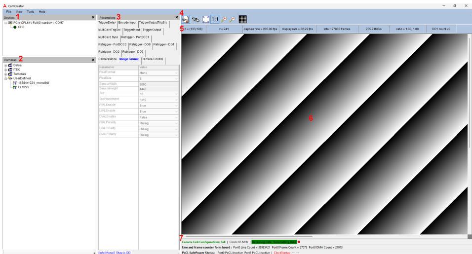
![Cam Creator\nFile View Tools Help\nDevices 1\nPC2a CPL46: Full(0) card=1, COM7\nCHD\nCamera 2\nDelete\nTEK\nTemplate\nUse=CideFred\n16384e1024_mono88\nCL9222\nParameters 3\nTriggerCenter (SyncInput) (TriggerOutputTrigBlue)\nMultiCardTropin (TriggerInput) (TriggerOutput)\nMultiCard Sets (Refrugar - PortDCC1)\nRefrugar - PortDCC2 (Refrugar - D00) (Refrugar - D01)\nRefrugar - D02 (Refrugar - D03)\nCameraMode Image Format Camera Control\nParameter Value\nProof format Marks -\nPosition 5\nSensorWidth 2560\nSensorHeight 1440\nTop 10\nTopPlacement Field\nPDLEnable True\nLVLEnable True\nDVLEnable False\nPDLPotarity Rising\nLVLPotarity Rising\nDVLPotarity Rising\nCamera Disk Configurations Full | Clock (5 MHz) \nUse and Frame counter formats board: Port1 Loss Count = 3385421 Port1 Frame Count = 27073 Port1 DMA Count = 27073\nPoCL SafePower Status: Port1PoCLInactive Port1PoCLInactive | ClickStartup :](.pcie-cpl64v-50m-18534-1000-10/9ff85c59f1c89ddb1b8e4b0bd313ee2fa741f9f9651094ba752aab18f5b6120e.jpg)

# 1. Devices panel

The list window displays the PCIe-CPL64V cards installed on the local computer.

# 2. Cameras panel

The tree browser window lists all available cameras and their camera files or user-defined camera files.

# 3. Parameters panel

The tab window lists all adjustable parameters.

# 4. Tool bar

The tool strip lists all adjustable parameters.

# 5. Status bar

The status bar shows the information about the captured image.

# 6. Display panel

This window shows captured image.

# 7. Board status strip

This board status strip shows the information about the board LED status, capture status, and PoCL status.

# 7.3 Operation Theory

CamCreator provides some preview functions for the PCIe-CPL64V Full card, as described below:

When opening CamCreator, the program automatically scans the system for cpl64v devices and displays them in the Device Panel.

Warning: When using multiple cards, please adjust the card ID. Please refer to Section 2.3.6

When selecting a device, please select the channel that needs to be activated. If this is your first time using CamCreator, the program will not automatically import the CAM file settings for you.

As mentioned above, when you select a CAM file from the Cameras Panel, CamCareator will save the current settings. Alternatively, you can customize your own CAM file by adjusting the appropriate parameters in the Parameter panel. Remember to click File Menu->”Save CAM file”.

# 7.3.1 Devices Panel

Currently, CamCreator does not support capturing images from multiple channels simultaneously. Please select the appropriate active channel to set up.
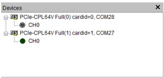
![Devices\nPCIe-CPL64V Full(0) cardid=0, COM28\nCH0\nPCIe-CPL64V Full(1) cardid=1, COM27\nCH0](.pcie-cpl64v-50m-18534-1000-10/52ee99a54a08bd9b981f7c8e87c838369c573baa6cd2ba27d419647d5fe169ba.jpg)

# Device

 The Device displays the PCIe-CPL64V device index, card index, and the system's corresponding COM number. Note: If another camera software that accesses the PCIe-CPL64V's COM port is opened first, the COM number will return -1.
 Warning: When using multiple cards, please adjust the card ID. Please refer to Section 2.3.6

# Current active channel

 All operations will apply to this channel.

# Inactive channel

 Click the channel after this icon to activate this channel. Only one channel can be active at one time. If you select standby channel, the current active channel will become inactive.

# Close this panel

# 7.3.2 Cameras Panel

Currently, only some template CAM files and some scenario references are provided. Please refer to Section 5.2.1- 5.2.5
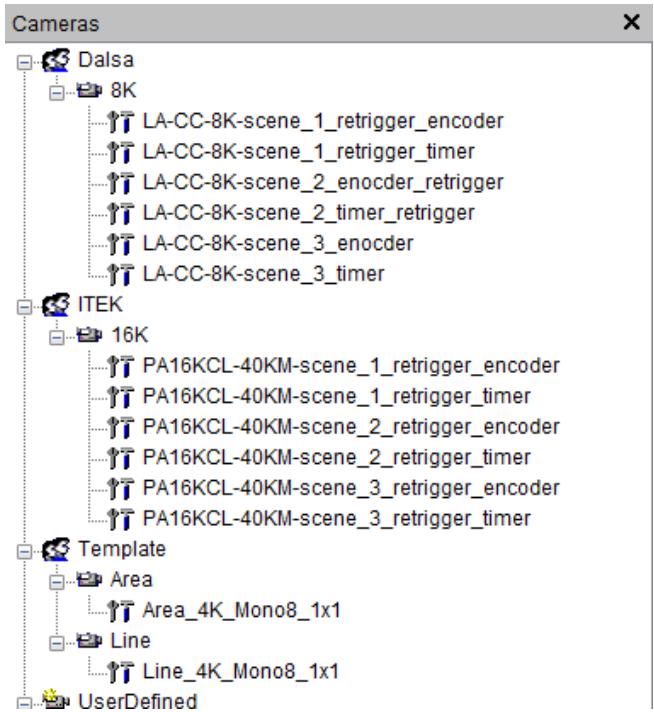
![Cameras\nDalsa\n8K\nLA-CC-8K-scene_1_retrigger_encoder\nLA-CC-8K-scene_1_retrigger_timer\nLA-CC-8K-scene_2_enocder_retrigger\nLA-CC-8K-scene_2_timer_retrigger\nLA-CC-8K-scene_3_enocder\nLA-CC-8K-scene_3_timer\nITEK\n16K\nPA16KCL-40KM-scene_1_retrigger_encoder\nPA16KCL-40KM-scene_1_retrigger_timer\nPA16KCL-40KM-scene_2_retrigger_encoder\nPA16KCL-40KM-scene_2_retrigger_timer\nPA16KCL-40KM-scene_3_retrigger_encoder\nPA16KCL-40KM-scene_3_retrigger_timer\nTemplate\nArea\nArea_4K_Mono8_1x1\nLine\nLine_4K_Mono8_1x1\nUserDefined](.pcie-cpl64v-50m-18534-1000-10/64bd1161463c4fb04f3883be9fcd9931dd3f68d193b9493a10974163ffe8ef08.jpg)

Camera provider
Camera type

# Camera file

# Current loaded camera file

 Select an appropriate camera file for your camera. CamCreator will load this camera file to the device and shows its parameters in the parameters panel.
 If you are using CamCreator for the first time, the utility will use the default settings of the current card until you select a camera CAM file.

Close this panel

# 7.3.3 Parameters Panel

The parameters panel shows the parameters of the selected camera file. Any modifications are applied immediately to the current active device. Users can save the camera file with the modified parameters by using the “Save Cam File” command in main menu.
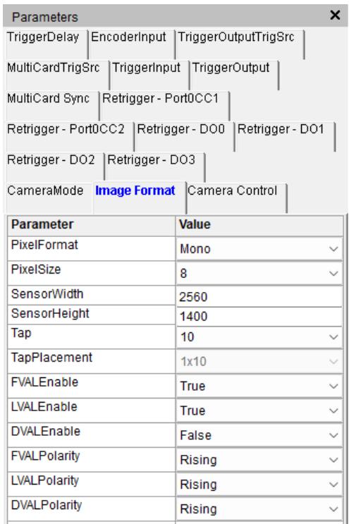
![Parameters\nTriggerDelay | EncoderInput | TriggerOutputTrigSrc |\nMultiCardTrigSrc | TriggerInput | TriggerOutput |\nMultiCard Sync | Retrigger - Port0CC1 |\nRetrigger - Port0CC2 | Retrigger - DO0 | Retrigger - DO1 |\nRetrigger - DO2 | Retrigger - DO3 |\nCameraMode Image Format Camera Control\nParameter Value\nPixelFormat Mono\nPixelSize 8\nSensorWidth 2560\nSensorHeight 1400\nTap 10\nTapPlacement 1x10\nFVALEnable True\nLVALEnable True\nDVALEnable False\nFVALPolarity Rising\nLVALPolarity Rising\nDVALPolarity Rising](.pcie-cpl64v-50m-18534-1000-10/460064e88bc0de3cb8ec5242b46c66df17e2c93b5198d25068d63aed98b8ae1d.jpg)

# Close this panel

# 7.3.4 Toolbar

![This image displays a computer file icon. It features a white, paper-like document background. Overlaid on the left side is a small rectangular thumbnail image showing a dark shape and yellow-green elements. On the bottom right corner, there is a large green triangle pointing to the right, resembling a play button. There is no text visible in the image.](.pcie-cpl64v-50m-18534-1000-10/42d9ec51321a8c06dc9ca57702c6b83740e0458927504d6ba2249d6da49c30a9.jpg)

# Continuous Grab

 Starts grabbing images and displays the images on the Display panel. Click it again to stop grabing. This is a toggle button.
 Warning: If your image does not conform to the supported format and restrictions, CamCreator will display a warning window. Please refer to Section 5.1.2

![The image features a stylized, pixelated illustration of an eye angled diagonally towards the upper right. It is set against a light blue gradient background. The eye has a thick black outline, a white sclera, a black pupil, and a teal-colored iris.](.pcie-cpl64v-50m-18534-1000-10/86b966c37741f9ccf30bbde8b9db00f393e3db3721e87b5ab82b3f143d0e12f5.jpg)

# Hide Image

 Hide or unhide the displayed image. This is a toggle button.

![The image shows a square icon featuring a light blue border. Inside the white square, there are four blue arrows pointing outward from the center toward each of the four corners.](.pcie-cpl64v-50m-18534-1000-10/103061052782fb24cd1b55270269b102821a2a60c456b60293914b45609a4a60.jpg)

# Fit Size

 Fit the image to the entire Display panel.

# 1:1

# Original Size

 Restores to the original size.

![An icon of a magnifying glass featuring a yellow handle and a white lens with a red plus sign inside, set against a light blue background.](.pcie-cpl64v-50m-18534-1000-10/b16549e291508e60c375aebe7dff1827c4a78241531f2a00965603be63f7ca50.jpg)

# Zoom In

 Zooms in the image

![The image displays a digital icon, likely a 'zoom out' button. It features a magnifying glass with a yellow handle and a white rim. Inside the lens is a red horizontal dash. The icon is set against a light blue gradient background.](.pcie-cpl64v-50m-18534-1000-10/6d6d90712282a6f2ad4579623a17dd990f3d34d8bccf6ac82b465475285c6a95.jpg)

# Zoom Out

 Zooms out the image

![The image displays a 4x4 grid composed of solid colored squares. The colors used are blue, green, and red. The arrangement follows a repeating pattern:\n- The top row consists of blue, green, green, and blue squares.\n- The second row consists of green, blue, red, and green squares.\n- The third row repeats the first row's pattern: blue, green, green, blue.\n- The fourth row repeats the second row's pattern: green, blue, red, green.](.pcie-cpl64v-50m-18534-1000-10/fef8942a3b6e5647c5df3fb7437a53b8917a815566510ffa7cb9ded823170ac0.jpg)

# Bayer Decoder

![Converts the Bayer pattern to RGB24 (Note: CamCreator only)\nDisables Bayer\nBayerBG\nBayerGB\nBayerGR\nBayerRG](.pcie-cpl64v-50m-18534-1000-10/019a619a5c43ee68a307c3f429525a1a2facf42777b261bdccce0ec454e267cc.jpg)

# 7.3.5 Status Bar

<table><tr><td>p = (0,0)</td><td>v = 0</td><td>capture rate = 0.0 fps</td><td>display rate = 0.0 fps</td><td>total : 0 frames</td><td>0MB/s</td><td>ratio = 1.00, 1.00</td><td>CC1 count =0</td></tr></table>

From left to right, the panel items are: cursor position, pixel value, frame rate, display rate, total captured frames, data transfer rate, magnification (horizontal ratio, vertical ratio) and CC1 count.

Note: The CC1 count is cleared after calling the Advanced Configuration API.(ResetDebugCount) or by clicking the “Reset All Statistics” button in the TriggerIOCounters form.

# 7.3.6 Display Panel

Click the left mouse button and drag to create a rectangular region on the Display panel, which will be zoomed in. If you hold Ctrl while dragging, the image will be zoomed in with equal width and height proportions. See example below:

![Abstract geometric design with a green rectangle and arrow, set against a gradient background (no text or symbols)](.pcie-cpl64v-50m-18534-1000-10/1cf88470f97b9ceca6cc0ebf3491e47e0e81d63781ada3453d4165f3385314a2.jpg)

Click the right mouse button, and the cursor will change to a move2D icon. The user can drag the image. As shown below:

![Abstract gradient background with a central diamond-shaped symbol, no text or symbols present](.pcie-cpl64v-50m-18534-1000-10/d0fb777445644112d0bc2c379e642e4c0f6f5d493aa7ca60b24f640255b24190.jpg)

From left to right, the bottom of the draw panel displays the following status indicators: CameraLink Configurations (Camera link not detected / Base / Medium / Full / Abnormal), front end device clock rate, whether the device is receiving data from the front end device (Green/Red), whether the device is transmitting data to the host (Green/Red), and Line count, frame count kernel DMA count, and PoCL SafePower Status. As shown below:

<table><tr><td>Camera Link Configurations: Camera link not detected | Clock: 85 MHz | Receiving Data Transmitting Data ○</td></tr><tr><td>Line and frame counter form board : Port0 Line Count = 0 Port0 Frame Count = 0 Port0 DMA Count = 0</td></tr><tr><td>PoCL SafePower Status : Port0 PoCL:Inactive Port1 PoCL:Inactive | -- -- --</td></tr></table>

Note: The PoCL SafePower Status indicates that the PoCL channel status is active or inactive and also shows any Power-over-Cameralink error. (-- -- --) indicates no error; if there is an error, it will display on of the following: (Clock Startup, Clock Drop, Voltage Below).

<table><tr><td></td><td>Receiving data</td><td>Receiving data</td></tr><tr><td>Transmitting data</td><td>Starts capturing, video stream is received by the FPGA, and the FPGA is transmitting the video stream data to the host</td><td>FPGA is not receiving the video stream from the front-end device, and continues to transmit the residual data stored internally within the FPGA to the host.</td></tr><tr><td>Transmitting data</td><td>Start capturing, video stream is received by the FPGA, but the FPGA is not transmitting the video stream data to the host</td><td>No video stream</td></tr></table>

Note: These are the debug status that can be used to retrieve the current frame grabber’s image acquisition status through the Advanced Configuration API.

<table><tr><td>Debug.DataStreamStatus</td><td>Bit 1</td><td>Bit 0</td><td>Description</td></tr><tr><td>`0` (`0b00`)</td><td>0</td><td>0</td><td>No data transfer</td></tr><tr><td>`1` (`0b01`)</td><td>0</td><td>1</td><td>Receiving data from front-end device only</td></tr><tr><td>`2` (`0b10`)</td><td>1</td><td>0</td><td>N/A</td></tr><tr><td>‘3’(‘0b11’)</td><td>1</td><td>1</td><td>Simultaneously receiving and transmitting data</td></tr></table>

# 7.3.7 Main Menu

# File Menu

# Open Cam File

 Load camera parameters from a camera file.

# Save Cam File

 Save the current camera parameters to the current loaded camera file.

# Save Cam File As

 Save the current camera parameters to a new camera file.

# Delete Cam File

 Delete the currently loaded camera file.

 Note: Template CAM file cannot be deleted.

# Save Image

 Save the currently displayed image as a raw and bitmap file.(RGB/MONO only)

# Exit

 Terminate CamCreator.

# View Menu

# Devices

 Hide or unhide the Devices panel.

# Cameras

 Hide or unhide the Cameras panel.

# Parameters

 Hide or unhide the Parameters panel.

# Tools Menu

# ￼ (TriggerIOCounters)

 Open the General I/O purpose, encoder counter, and trigger event statistics. All the values can also be accessed through the Advanced Configuration API. For details, please refer to Chapter 6.

![Trigger10Counters\nTriggerInput\nStatus\n0 1 2 3 Get\nDI ○ ○ ○ ○\nCommand\n1 Software Trigger\nStatistics\nTriggerSource DelayBuffer (Advanced)\nAddress Name Counts\n0x191C DOOTriggerEventCount 0\n0x191D DOOTriggerDropCount 0\n0x191E DOITriggerEventCount 0\n0x191F DOITriggerDropCount 0\n0x1920 DOZTriggerEventCount 0\n0x1921 DOZTriggerDropCount 0\n0x1922 DO3TriggerEventCount 0\n0x1923 DO3TriggerDropCount 0\n0x19308 Port0CC1TriggerEventCount 0\n0x1939 Port0CC1TriggerDropCount 0\n0x193A Port0CC2TriggerEventCount 0\n0x193B Port0CC2TriggerDropCount 0\nDelay\nStatistics\nAddress Name Counts\n0x181B DOORetriggerEventCount 0\n0x1819 DOORetriggerDropCount 0\n0x181A DOIRetriggerEventCount 0\n0x181B DOIRetriggerDropCount 0\n0x181C DOZRetriggerEventCount 0\n0x181D DOZRetriggerDropCount 0\n0x181E DO3RetriggerEventCount 0\n0x181F DO3RetriggerDropCount 0\n0x1820 Port0CC1RetriggerEventCount 0\n0x1821 Port0CC1RetriggerDropCount 0\n0x1822 Port0CC2RetriggerEventCount 0\n0x1823 Port0CC2RetriggerDropCount 0\nRetrigger\nStatistics\nAddress Name Counts\n0x192B DOOTriggerOutEventCount 0\n0x1929 DOOTriggerOutDropCount 0\n0x193A DOITriggerOutEventCount 0\n0x193B DOITriggerOutDropCount 0\n0x193C DOZTriggerOutEventCount 0\n0x193D DOZTriggerOutDropCount 0\n0x193E DOITriggerOutEventCount 0\n0x193F DOITriggerOutDropCount 0\nTriggerOutput\nDO Status\nstatus ■ ■ ■ ■ ■ ■ ■ ■ ■ ■ ■ ■ ■ ■ ■ ■ ■ ■ ■ ■ ■ ■ ■ ■ ■ ■ ■ ■ ■ ■ ■ ■ ■ ■ ■ ■ ■ ■ ■ ■ ■ ■ ■ ■ ■ ■ ■ ■ ■ ■ ■ ■ ■ ■ ■ ■ ■ ■ ■ ■ ■ ■ ■ ■ ■ ■ ■ ■ ■ ■ ■ ■ ■ ■ ■ ■ ■ ■ ■ ■ ■ ■ ■ ■ ■ ■ ■ ■ ■ ■ ■ ■ ■ ■ ■ ■ ■ ■ ■ ■ □□□□□□□□□□□□□□□□□□□□□□□□□□□□□□□□□□□□□□□□□□□□□□□□□□□□□□□□□□□□□□□□□□□□□□□□□□□□□□□□□□□□□□□□□□□□□□□□□□□□□○○○○○○○○○○○○○○○○○○○○○○○○○○○○○○○○○○○○○○○○○○○○○○○○○○○○○○○○○○○○○○○○○○○○○○○○○○○○○○○○○○○○○○○○○○○○○○○○○○○○● Reset All Statistics\nEncoder\nEncoder Value\n0 Write Value\nCameraControl\nCC19status - CC29status\nstatus □ □ □ □ □ □ □ □ □ □ □ □ □ □ □ □ □ □ □ □ □ □ □ □ □ □ □ □ □ □ □ □ □ □ □ □ □ □ □ □ □ □ □ □ □ □ □ □ □ □ ▢](.pcie-cpl64v-50m-18534-1000-10/e2782e9ca13c83c9d87dbafac6fc07ab5a36172fe1a85a35bf81bfb410ad74fc.jpg)

# Help Menu

# About CamCreator

 Show the CamCreator version.

# About Device

 Show device information.
 Show SDK version.

# 8 Firmware Update

ADLINK provides a firmware update tool that helps users to update the firmware when necessary.

# 8.1 Firmware Update Procedures

1. Run "FirmwareUpdate.exe" in the installation directory.

![File\nHome\nShare\nView\nManage\nFirmwareTool\nApplication Tools\nThis PC ) Local Disk (C:) ) Program Files ) ADLINK ) AWS ) FirmwareTool\nQuick access\nThis PC\nNetwork\nplatforms\nFirmwareUpdate.\nexe\nQt5Core.dll\nQt5Gui.dll](.pcie-cpl64v-50m-18534-1000-10/03991812c2a8c78512f9b41cd48bd68ed4c482167ebdfaf2afd90b6d3c43e67f.jpg)

2. Click "Scan Device", select the "PCIe-CPL64V Full" that needs to be updated, and then click "Select the \*.bin" to choose the firmware file to update.

![Firmware Update Tool\n1 Devices\nScan Device\nPCIe Devices\nPCIe-CPL64V Full index: 0\nSelect the *.bin\n2\n0%\n3\nFirmware Remote Update\nNew folder\nOrganize\nOpen File\nFile name: cpl64v_top_20251022_00001800_A2_working.bir\nFirmware file: .bir\nOpen\nCancel\nMessage Logs\n(2025-11-05 10:50:14) Selected Device Index: 0, Device ID: 0, Firmware Version:\n20251022_1800\nClear Log\n4\nName\nDate modified\ncpl64v_top_20251022_00001800_A2_working.bin\n10/31/2025 10:43 A](.pcie-cpl64v-50m-18534-1000-10/1123caa488e4b28a0bc44b8a70b43bb4c76b4d5165b6890be010e7498a1a7ffa.jpg)

3. After confirming the file, click to start the firmware update.

![Firmware Update Tool\nDevices\nScan Device\nPCIe Devices\nPCIe-CPL64V Full index: 0\nFirmware Remote Update\nSelect the *.bin\n0%\nConfirm File\nSelected file:\nC:/Users/IMB-M47-R680E/Desktop/PCIe-CPL64V Full FPGA/\ncpl64v_top_20251022_00001800_A2_working_1MMCM/\ncpl64v_top_20251022_00001800_A2_working.bin\nContinue?\nOK Cancel\nClear Log](.pcie-cpl64v-50m-18534-1000-10/666139b6fb4c757bc2efeed81f60a03cbeefbe1ccd693ed36770dda2d4bef061.jpg)

4. After the update is completed, please cold boot the system.

![Firmware Update Tool\nDevices\nScan Device\nPCIe Devices\nPCIe-CPL64V Full index: 0\nFirmware Remote Update\nSelect the *.bin\n100%\nMessage Logs\n(2025-11-05 16:52:23) Write 2b0000\n(2025-11-05 16:52:23) Write 2c0000\n(2025-11-05 16:52:23) Write 2d0000\n(2025-11-05 16:52:23) Write 2e0000\n(2025-11-05 16:52:23) Write complete. Please shutdown (Cold start) your system!\nClear Log](.pcie-cpl64v-50m-18534-1000-10/e93a25c6713fdda69cfa1d2f596cc99d04992db51c6865e669df47308792948d.jpg)

# Safety Instructions

Read and follow all instructions marked on the product and in the documentation before you operate your system. Retain all safety and operating instructions for future use.

Please read these safety instructions carefully.
• Please keep this User‘s Manual for later reference.
• Read the specifications section of this manual for detailed information on the operating environment of this equipment.
• When installing/mounting or uninstalling/removing equipment, turn off the power and unplug any power cords/cables.
• To avoid electrical shock and/or damage to equipment:

Keep equipment away from water or liquid sources.
Keep equipment away from high heat or high humidity.
 Keep equipment properly ventilated (do not block or cover ventilation openings).
 Make sure to use recommended voltage and power source settings.
 Always install and operate equipment near an easily accessible electrical socket-outlet.
Secure the power cord (do not place any object on/over the power cord).
 Only install/attach and operate equipment on stable surfaces and/or recommended mountings.
 If the equipment will not be used for long periods of time, turn off and unplug the equipment from its power source.

• Never attempt to fix the equipment. Equipment should only be serviced by qualified personnel.

For indoor use only.

Altitude during operation: up to 2000 m.

Over voltage category: OVC II

Pollution degree: 2

Ingress protection: X0

# Getting Service

Ask an Expert: https://www.adlinktech.com/en/Askanexpert

# ADLINK Technology, Inc.

Address: No. 66, Huaya 1st Road, Guishan District Taoyuan City 333, Taiwan

Tel: +886-3-216-5088

Fax: +886-3-328-5723

Email: service@adlinktech.com

# Ampro ADLINK Technology, Inc.

Address: 6450 Via Del Oro, San Jose, CA 95119-1208, USA

Tel: +1-408-360-0200

Toll Free: +1-800-966-5200 (USA only)

Fax: +1-408-600-1189

Email: info@adlinktech.com

# ADLINK Technology (China) Co., Ltd.

Address: 300 Fang Chun Rd., Zhangjiang Hi-Tech Park, Pudong New Area Shanghai, 201203 China

Tel: +86-21-5132-8988

Fax: +86-21-5132-3588

Email: market@adlinktech.com

# ADLINK Technology GmbH

Address: Hans-Thoma-Strasse 8-10, 68163 Mannheim, Germany

Tel: +49-621-43214-0

Fax: +49-621 43214-30

Email: emea@adlinktech.com

Please visit the Contact page at www.adlinktech.com for information on how to contact the ADLINK regional office nearest you.
[🔗 Link to the original document](.pcie-cpl64v-50m-18534-1000-10/pcie-cpl64v-50m-18534-1000-10.pdf)