# PCIS-DASK

Data Acquisition Software Development Kit for NuDAQ® PCI Bus Cards

User's Manual

Manual Rev. 2.00

Revision Date: March 05, 2007

Part No: 50-11224-2000

![The image displays a black circle containing the universal recycling symbol, also known as the Mobius loop. Inside the circle are three white arrows arranged in a triangular formation, chasing each other in a clockwise direction. Each arrow features three horizontal stripes near its tail end.](.pcis-dask-manual-3/6180fb380b5c4a80f5533286de5df1c3ed67595ecb83526e915577e4a73a5bb3.jpg)
Recycled Paper

Copyright 2007 ADLINK TECHNOLOGY INC.

All Rights Reserved.

# Disclaimer

The information in this document is subject to change without prior notice in order to improve reliability, design, and function and does not represent a commitment on the part of the manufacturer.

In no event will the manufacturer be liable for direct, indirect, special, incidental, or consequential damages arising out of the use or inability to use the product or documentation, even if advised of the possibility of such damages.

This document contains proprietary information protected by copyright. All rights are reserved. No part of this manual may be reproduced by any mechanical, electronic, or other means in any form without prior written permission of ADLINK.

# Trademark Information

NuDAQ is a registered trademark of ADLINK Technology Inc.

Product names mentioned herein are used for identification purposes only and may be trademarks and/or registered trademarks of their respective companies.

# Getting service

Customer satisfaction is our top priority. Contact us should you require any service or assistance.

# ADLINK TECHNOLOGY INC.

Web Site http://www.adlinktech.com

Sales & Service service@adlinktech.com

Telephone No. +886-2-8226-5877

Fax No. +886-2-8226-5717

Mailing Address 9F No. 166 Jian Yi Road, Chungho City,

Taipei Hsien 235, Taiwan, ROC

# ADLINK TECHNOLOGY AMERICA, INC.

Sales & Service info@adlinktech.com

Toll-Free +1-866-4-ADLINK (235465)

Fax No. +1-949-727-2099

Mailing Address 8900 Research Drive, Irvine, CA 92618, USA

# ADLINK TECHNOLOGY EUROPEAN SALES OFFICE

Sales & Service emea@adlinktech.com

Toll-Free +49-211-4955552

Fax No. +49-211-4955557

Mailing Address Nord Carree 3, 40477 Düsseldorf, Germany

# ADLINK TECHNOLOGY SINGAPORE PTE LTD

Sales & Service singapore@adlinktech.com

Telephone No. +65-6844-2261

Fax No. +65-6844-2263

Mailing Address 84 Genting Lane #07-02A, Cityneon Design

Center, Singapore 349584

# ADLINK TECHNOLOGY INDIA LIAISON OFFICE

Sales & Service india@adlinktech.com

Telephone No. +91-80-57605817

Fax No. +91-80-26671806

Mailing Address No. 1357, Ground Floor, "Anupama",

Aurobindo Marg JP Nagar (Ph-1)

Bangalore - 560 078

# ADLINK TECHNOLOGY BEIJING

Sales & Service market@adlinkchina.com.cn

Telephone No. +82-2-20570565

Fax No. +82-2-20570563

Mailing Address 4F, Kostech Building, 262-2, Yangjae-Dong,

Seocho-Gu, Seoul, 137-130, Korea

# ADLINK TECHNOLOGY BEIJING

Sales & Service market@adlinkchina.com.cn

Telephone No. +86-10-5885-8666

Fax No. +86-10-5885-8625

Mailing Address Room 801, Building E, Yingchuangdongli Plaza, No.1 Shangdidonglu, Haidian District, Beijing, China

# ADLINK TECHNOLOGY SHANGHAI

Sales & Service market@adlinkchina.com.cn

Telephone No. +86-21-6495-5210

Fax No. +86-21-5450-0414

Mailing Address Floor 4, Bldg. 39, Caoheting Science and

Technology Park, No.333 Qinjiang Road,

Shanghai, China

# ADLINK TECHNOLOGY SHENZHEN

Sales & Service market@adlinkchina.com.cn

Telephone No. +86-755-2643-4858

Fax No. +86-755-2664-6353

Mailing Address C Block, 2nd Floor, Building A1,
Cyber-tech Zone, Gaoxin Ave. 7.S,
High-tech Industrial Park S., Nanshan District,
Shenzhen, Guangdong Province, China

# Using this manual

# Audience and scope

This manual guides you when using the PCIS-DASK software driver for NuDAQ PCI bus data acquisition cards. This manual also describes how to install and use the software library and meet your requirements when creating programs for your software applications.

# How this manual is organized

This manual is organized as follows:

Chapter 1 Introduction: This chapter introduces the PCIS-DASK and lists all DAQ modules and language environments which the program supports.

Chapter 2 Function Classes: This chapter describes the classes of functions which the PCIS-DASK supports.

Chapter 3 Building Applications: This section describes the fundamentals of building PCIS-DASK applications in Windows and Linux.

Chapter 4 Application Hints: This chapter provides the PCIS-DASK programming schemes for various DAQ operations.

Chapter 5 Continuous Data Transfer: This section illustrates the mechanism and techniques that PCIS-DASK uses for continuous data transfer.

Chapter 6 Utilities: This chapter describes the Win32 and PCIS-DASK/X utilities.

Chapter 7 Sample Programs: This chapter provides some PCIS-DASK sample programs for supported module

Chapter 8 Distribution of Applications: This section lists the files, installers, and manual installation procedures needed when distributing your PCIS-DASK-based applications.

# Conventions

Take note of the following conventions used throughout the manual to make sure that you perform certain tasks and instructions properly.

NOTE Additional information, aids, and tips that help you perform particular tasks.

IMPORTANT Critical information and instructions that you MUST perform to complete a task.

WARNING Information that prevents physical injury, data loss, module damage, program corruption etc. when trying to complete a particular task.

# Table of Contents

# 1 Introduction ...... 1

1.1 Hardware Support.... 2
1.2 Language Support 3

# 2 Function Classes.... 5

2.1 General Configuration Function Group 6
2.2 Actual Sampling Rate Function Group 6
2.3 Analog Input Function Group 7

Analog Input Configuration Functions 7
One-Shot Analog Input Functions 9
Continuous Analog Input Functions 9
Asynchronous Analog Input Monitoring Functions ..... 11

2.4 Analog Output Function Group 12

Analog Output Configuration Functions 12
One-Shot Analog Output Functions 13

2.5 Digital Input Function Group 14

Digital Input Configuration Functions 14
One-Shot Digital Input Functions 14
Continuous Digital Input Functions 15
Asynchronous Digital Input Monitoring Functions ...... 16

2.6 Digital Output Function Group 17

Digital Output Configuration Functions 17
One-Shot Digital Output Functions 18
Continuous Digital Output Functions 19
Asynchronous Digital Output Monitoring Functions ..... 19

2.7 Timer/Counter Function Group 20

Timer/Counter Functions 20
General-Purpose Timer/Counter Functions 20

2.8 Digital Input/Output Function Group 22

Digital Input/Output Configuration Functions 22
Dual-Interrupt System Setting Functions 23
Local Interrupt Setting Functions 24

2.9 Emergency Shutdown Function Group 25

2.10 Watchdog Timer Function Group 25
2.11 Hot-system Reset Hold Function Group 25
2.12 Calibration Function Group 25

# 3 Building Applications 27

3.1 Contiguous Memory Allocation 27
3.2 Application Building Fundamentals in Windows 28

Using Microsoft® Visual C®/C++® 28

Using Microsoft® Visual Basic® 29

3.3 Application Building Fundamentals in Linux 32
3.4 Application Building Fundamentals Using .NET 33

Using Microsoft VB.net. 33

Using Microsoft C# 35

Creating Windows® PCIS-DASK Application Using Microsoft VB.net. 37

Using Callback Functions in a VB.net Application with PCIS-DASK 38

Using Callback Functions in a C# Application with PCIS-DASK 39

# 4 Application Hints 41

4.1 Analog Input 42

One-Shot Analog Input 43

Synchronous Continuous Analog Input 44

Non-Trigger Non-double-buffered Asynchronous Continuous Analog Input 45

Non-Trigger Double-buffered Asynchronous Continuous Analog Input 47

Trigger Mode Non-double-buffered Asynchronous Continuous Analog Input 49

Trigger Mode Double-buffered Asynchronous Continuous Analog Input 51

4.2 Analog Output Programming Hints 54
4.3 Digital Input Programming Hints 55

One-Shot Digital Input 56

Synchronous Continuous Digital Input 58

Non-double-buffered Asynchronous Continuous Digital Input 59

Double-buffered Asynchronous Continuous
Digital Input ....61

Multiple-buffered Asynchronous Continuous Digital Input 63

4.4 Digital Output Programming Hints 66

One-Shot Digital Output 67

Synchronous Continuous Digital Output 69

Asynchronous Continuous Digital Output 70

Pattern Generation Digital Output 71

Multiple-buffered Asynchronous Continuous Digital Output 72

4.5 DAQ Event Message Programming Hints 74

4.6 Interrupt Event Message Programming Hints.... 76

# 5 Continuous Data Transfer 79

5.1 Mechanisms.... 79

5.2 Double-Buffered AI/DI Operation 80

Double Buffer Mode Principle 80

Single-Buffered Versus Double-Buffered Data Transfer 82

5.3 Trigger Mode Data Acquisition for Analog Input 83

# 6 Utilities 85

6.1 Win32 Utilities 85

NuDAQ Registry/Configuration (PciUtil) 85

Data File Converter (DAQCvt) 89

Sample Programs Browser 92

6.2 PCIS-DASK/X Utilities 93

dask\_conf 93

6.3 Module Installation Script.... 96

6.4 Uninstallation Script 98

6.5 Data File Converter (DAQCvt) 98

Options for data format conversion 99

Options for separator in text file 99

Options for Title/Head in text file 99

# 7 Sample Programs.... 101

7.1 Brief Program Descriptions.... 101

7.2 Development Environments.... 116

Visual Basic Sample Programs 116

Microsoft C/C++ Sample Programs 116

7.3 Execute Sample Programs.... 118

7.4 Detailed Descriptions of Programs 119

A/D Conversion, D/A Conversion, D/I, and D/O ..... 120

Data I/O Through DMA Data Transfer or Interrupt Operation 121

Double Buffer Mode Data I/O Through DMA Transfer or Interrupt Operation .... 122

Trigger Mode Data I/O Through DMA Data
Transfer or Interrupt Operation .... 123

# 8 Distribution of Applications.... 125

8.1 Required Files.... 125
8.2 Automatic Installers.... 127
8.3 Manual Installation.... 128

# 1 Introduction

The PCIS-DASK is a software development kit for NuDAQ data acquisition cards utilizing the PCI bus. With high performance data acquisition driver, the PCIS-DASK lets you develop custom applications under Windows® NT/98/2000/XP/Server 2003 and Linux environments.

With memory and data buffer management capabilities, the PCIS-DASK gives you freedom from dealing with complex issues and focus more on developing your applications. The PCIS-DASK also implements simple communication with NuDAQ PCI-bus cards, while the easy-to-use functions allow you to utilize all the card's features in a high-level way.

The PCIS-DASK also delivers you the advantage of all the power features of Microsoft® Win32 System and Linux for your data acquisition applications, including running multiple applications and using extended memory. The PCIS-DASK's flawless support for Visual Basic environment makes it easy to create custom user interfaces and graphics.

In addition to the software drivers, the PCIS-DASK comes with sample programs for your reference. These sample programs help you develop your applications quickly and conveniently.

# 1.1 Hardware Support

The PCIS-DASK currently supports the following NuDAQ data acquisition and NuIPC CompactPCI cards:

▶ PCI-6208A/cPCI-6208A ▶ PCI-7432/cPCI-7432
▶ PCI-6208V/16V/cPCI-6208V ▶ PCI-7433/cPCI-7433
▶ PCI-6308A ▶ PCI-7434/cPCI-7434
▶ PCI-6308V ▶ cPCI-7432R
▶ PCI-7200/cPCI-7200 ▶ cPCI-7433R
▶ PCI-7230/cPCI-7230 ▶ cPCI-7434R
▶ PCI-7233/PCI-7233H ▶ PCI-7442
▶ PCI-7234 ▶ PCI-7443
▶ PCI-7224 ▶ PCI-7444
▶ PCI-7248/cPCI-7248 ▶ cPCI-7452
▶ cPCI-7249R ▶ PCI-8554
▶ PCI-7250 ▶ PCI-9111
▶ cPCI-7252
▶ PCI-9112/cPCI-9112
▶ PCI-7256 ▶ PCI-9113
▶ PCI-7258 ▶ PCI-9114
▶ PCI-7260 ▶ cPCI-9116
▶ PCI-7296 ▶ PCI-9118
▶ PCI-7300A/cPCI-7300A ▶ PCI-9221
▶ PCI-7348 ▶ PCI-9812/10
PCI-7396

<table><tr><td>NOTE</td><td>ADLINK periodically upgrades the PCIS-DASK for new cards/modules. Check the card/modules’s Release Notes to know if PCIS-DASK supports it.</td></tr></table>

# 1.2 Language Support

The PCIS-DASK is a DLL (Dynamic-Link Library) version for use-with Windows $^{®}$ and Linux environments. It works with any Windows programming language that allows calls to a DLL. These include Microsoft $^{®}$ Visual C/C++ (4.0 or higher versions), Borland C++ (5.0 or higher versions), or Microsoft $^{®}$ Visual Basic (4.0 or higher version). In Linux, it works with any 32-bit compiler, such as gcc.

The PCIS-DASK also comes with a prototype function that supports Borland Delphi 2.x (32-bit) or higher versions.

# 2 Function Classes

This chapter describes the classes of functions that the PCIS-DASK supports.

All PCIS-DASK functions are grouped into different classes:

▶ General Configuration Function Group
▶ Actual Sampling Rate Function Group
▶ Analog Input Function Group
▷ Analog Input Configuration Functions
▶ One-Shot Analog Input Functions
▷ Continuous Analog Input Functions
▷ Asynchronous Analog Input Monitoring Functions

▶ Analog Output Function Group

▶ Digital Input Function Group

▶ Digital Input Configuration Functions
▶ One-Shot Digital Input Functions
▷ Continuous Digital Input Functions
▷ Asynchronous Digital Input Monitoring Functions

▶ Digital Output Function Group

▶ Digital Output Configuration Functions
▶ One-Shot Digital Output Functions
▷ Continuous Digital Output Functions
▷ Asynchronous Digital Output Monitoring Functions

▶ Timer/Counter Function Group

▶ DIO Function Group

▷ Digital Input/Output Configuration Functions
▷ Dual-Interrupt System Setting Functions
▷ Local Interrupt Setting Functions

Emergency Shutdown Function Group

▶ Watchdog Timer Function Group

▶ Hot-system Reset Hold Function Group

▶ Calibration Function Group

# 2.1 General Configuration Function Group

These functions initialize and configure data acquisition cards.

<table><tr><td>Register_Card</td><td>Initializes the hardware and software states of a NuDAQ PCI-bus data acquisition card. This function must be called before any other DASK library functions.</td></tr><tr><td>Release_Card</td><td>Tells the DASK library that the registered card is not in use and can be released. This function makes room for a new card to register.</td></tr><tr><td>GetCardType</td><td>Gets the card type of the device with a specified card index.</td></tr><tr><td>GetCardIndexFromID</td><td>Gets the card type and the sequence number of the device with a specified card ID.</td></tr><tr><td>GetBaseAddr</td><td>Gets the I/O base addresses of the device with a specified card index.</td></tr><tr><td>GetLCRAddr</td><td>Gets the LCR base address (defined by the PCI controller on board) of the device with a specified card index.</td></tr><tr><td>SetInitPattern</td><td>Sets the state of the initial or safety-out pattern.</td></tr><tr><td>GetInitPattern</td><td>Gets the state of relays set by the onboard switches.</td></tr><tr><td>IdentifyLED_Control</td><td>Controls identification LED.</td></tr></table>

# 2.2 Actual Sampling Rate Function Group

GetActualRate Returns the actual sampling rate the device will perform for the defined sampling rate value.

# 2.3 Analog Input Function Group

Analog Input Configuration Functions

<table><tr><td>AI_9111_Config</td><td>Informs PCIS-DASK library of the trigger source and trigger mode selected for the analog input operation of PCI9-111. You must call this function before calling function to perform continuous analog input operation of PCI-9111.</td></tr><tr><td>AI_9112_Config</td><td>Informs PCIS-DASK library of the trigger source selected for the analog input operation of PCI-9112. You must call this function before calling function to perform continuous analog input operation of PCI-9112.</td></tr><tr><td>AI_9113_Config</td><td>Informs PCIS-DASK library of the trigger source selected for the analog input operation of PCI-9113. You must call this function before calling function to perform continuous analog input operation of PCI-9113.</td></tr><tr><td>AI_9114_Config</td><td>Informs PCIS-DASK library of the trigger source selected for the analog input operation of PCI-9114. You must call this function before calling function to perform continuous analog input operation of PCI-9114.</td></tr><tr><td>AI_9116_Config</td><td>Informs PCIS-DASK library of the trigger source, trigger mode, input mode, and conversion mode selected for the analog input operation of PCI-9116. You must call this function before calling function to perform continuous analog input operation of PCI-9116.</td></tr><tr><td>AI_9118_Config</td><td>Informs PCIS-DASK library of the trigger source, trigger mode, input mode, and conversion mode selected for the ana-log input operation of PCI9118. You must call this function before calling function to perform continuous analog input operation of PCI-9118.</td></tr><tr><td>AI_9221_Config</td><td>Informs PCIS-DASK library of the trigger source, trigger mode, and trigger properties selected for the analog input operation of PCI-9221. You must call this function before calling function to perform continuous analog input operation of PCI-9221.</td></tr><tr><td>AI_9812_Config</td><td>Informs PCIS-DASK library of the trigger source, trigger mode, and trigger properties selected for the analog input operation of PCI-9812. You must call this function before calling function to perform continuous analog input operation of PCI-9812.</td></tr><tr><td>AI_9116_CounterInterval</td><td>Informs PCIS-DASK library of the scan interval value and sample interval value selected for the analog input operation of PCI-9116. You must call this function before calling function to perform continuous analog input operation of PCI-9116.</td></tr><tr><td>AI_9221_CounterInterval</td><td>Informs PCIS-DASK library of the scan interval value and sample interval value selected for the analog input operation of PCI-9221. You must call this function before calling function to perform continuous analog input operation of PCI-9221.</td></tr><tr><td>AI_InitialMemoryAllocated</td><td>Gets the actual size of analog input memory that is available in the device driver.</td></tr></table>

# AI\_GetView

Gets the mapped buffer address of the analog input memory that is available in the device driver.

# AI\_SetTimeOut

Sets the Timeout period for Sync mode of continuous AI.

One-Shot Analog Input Functions

<table><tr><td>AI_ReadChannel</td><td>Performs a software triggered A/D conversion (analog input) on an analog input channel and returns the value converted (unscaled).</td></tr><tr><td>AI_VReadChannel</td><td>Performs a software triggered A/D conversion (analog input) on an analog input channel and returns the value scaled to a voltage in units of volts.</td></tr><tr><td>AI_ReadMultiChannels</td><td>Performs software triggered A/D conversions on the specified analog input channels.</td></tr><tr><td>AI_ScanReadChannels</td><td>Performs software triggered A/D conversions on the specified analog input channels.</td></tr><tr><td>AI_VoltScale</td><td>Converts the result from an AI_ReadChannel call to the actual input voltage.</td></tr></table>

Continuous Analog Input Functions

<table><tr><td>AI_ContReadChannel</td><td>Performs continuous A/D conversions on the specified analog input channel at a rate as close to the rate you specified.</td></tr><tr><td>AI_ContScanChannels</td><td>Performs continuous A/D conversions on the specified continuous analog input channels at a rate as close to the rate you specified. This function is only available for those cards that support auto-scan functionality.</td></tr></table>

# AI\_ContReadMultiChannels

Performs continuous A/D conversions on the specified analog input channels at a rate as close to the rate you specified. This function is only available for those cards that support auto-scan functionality.

# AI\_ContReadChannelToFile

Performs continuous A/D conversions on the specified analog input channel at a rate as close to the rate you specified and saves the acquired data in a disk file.

# AI\_ContScanChannelsToFile

Performs continuous A/D conversions on the specified continuous analog input channels at a rate as close to the rate you specified and saves the acquired data in a disk file. This function is only available for those cards that support auto-scan functionality.

# AI\_ContReadMultiChannelsToFile

Performs continuous A/D conversions on the specified analog input channels at a rate as close to the rate you specified and saves the acquired data in a disk file. This function is only available for those cards that support auto-scan functionality.

# AI\_ContVScale

Converts the values of an array of acquired data from an continuous A/D conversion call to the actual input voltages.

# AI\_ContStatus

Checks the current status of the continuous analog input operation.

# AI\_EventCallBack

Controls and notifies the user's application when a specified DAQ event occurs.

<table><tr><td></td><td>The notification is performed through a user-specified callback function.</td></tr><tr><td>AI_ContBufferReset</td><td>Resets all the buffers set by function “AI_ContBufferSetup” for continuous analog input.</td></tr><tr><td>AI_ContBufferSetup</td><td>Sets up a specified buffer for continuous analog input.</td></tr></table>

Asynchronous Analog Input Monitoring Functions

<table><tr><td>AI_AsyncCheck</td><td>Checks the current status of the asynchronous analog input operation.</td></tr><tr><td>AI_AsyncClear</td><td>Stops the asynchronous analog input operation.</td></tr><tr><td>AI_AsyncDblBufferMode</td><td>Enables or disables double buffer data acquisition mode.</td></tr></table>

AI\_AsyncDblBufferHalfReady

<table><tr><td></td><td>Checks whether the next half buffer of data in circular buffer is ready for transfer during an asynchronous double-buffered analog input operation.</td></tr></table>

AI\_AsyncDblBufferTransfer

<table><tr><td></td><td>Copies half of the data of circular buffer to user buffer. You can execute this function repeatedly to return sequential half buffers of the data.</td></tr></table>

AI\_AsyncDblBufferOverrun

<table><tr><td></td><td>Checks or clears overrun status of the double-buffered analog input operation.</td></tr></table>

AI\_AsyncDblBufferHandled

<table><tr><td></td><td>Notifies the PCIS-DASK that the ready buffer has been handled in user application.</td></tr></table>

AI\_AsyncDblBufferToFile

<table><tr><td></td><td>Logs the data of the circular buffer to a disk file.</td></tr></table>

# 2.4 Analog Output Function Group

Analog Output Configuration Functions

<table><tr><td>AO_6208A_Config</td><td>Informs PCIS-DASK library of the current range selected for the analog output operation of PCI-6208A. You must call this function before calling function to perform current output operation.</td></tr><tr><td>AO_6308A_Config</td><td>Informs PCIS-DASK library of the current range selected for the analog output operation of PCI-6308A. You must call this function before calling function to perform current output operation.</td></tr><tr><td>AO_6308V_Config</td><td>Informs PCIS-DASK library of the polarity (unipolar or bipolar) that the output channel is configured for the analog output and the reference voltage value selected for the analog output channel(s) of PCI-6308V. You must call this function before calling function to perform current output operation.</td></tr><tr><td>AO_9111_Config</td><td>Informs PCIS-DASK library of the polarity (unipolar or bipolar) that the output channel is configured for the analog output of PCI-9111. You must call this function before calling function to perform voltage output operation.</td></tr><tr><td>AO_9112_Config</td><td>Informs PCIS-DASK library of the reference voltage value selected for the analog output channel(s) of PCI-9112. You must call this function before calling function to perform voltage output operation.</td></tr></table>

# One-Shot Analog Output Functions

<table><tr><td>AO_WriteChannel</td><td>Writes a binary value to the specified analog output channel.</td></tr><tr><td>AO_VWriteChannel</td><td>Accepts a voltage value, scales it to the proper binary value and writes a binary value to the specified analog output channel.</td></tr><tr><td>AO_VoltScale</td><td>Scales a voltage to a binary value.</td></tr><tr><td>AO_SimuWriteChannel</td><td>Writes binary values to the specified analog output channels simultaneously.</td></tr><tr><td>AO_SimuVWriteChannel</td><td>Accepts voltage values, scales them to the proper binary values and writes binary values to the specified analog output channels simultaneously.</td></tr></table>

# 2.5 Digital Input Function Group

Digital Input Configuration Functions

<table><tr><td>DI_7200_Config</td><td>Informs PCIS-DASK library of the trigger source and trigger properties selected for the digital input operation of PCI-7200. You must call this function before calling function to perform continuous digital input operation of PCI-7200.</td></tr></table>

DI\_7300A\_Config

<table><tr><td>DI_7300B_Config</td><td>Informs PCIS-DASK library of the trigger source and trigger properties selected for the digital input operation of PCI-7300A Rev.A or PCI-7300A Rev.B. You must call this function before calling function to perform continuous digital input operation of PCI-7300A Rev.A or PCI-7300A Rev.B.</td></tr></table>

DI\_InitialMemoryAllocated Gets the actual size of digital input DMA memory that is available in the device driver.

<table><tr><td>DI_GetView</td><td>Gets the mapped buffer address of the digital input memory that is available in the device driver.</td></tr></table>

One-Shot Digital Input Functions

<table><tr><td>DI_ReadLine</td><td>Reads the digital logic state of the specified digital line in the specified port.</td></tr><tr><td>DI_ReadPort</td><td>Reads digital data from the specified digital input port.</td></tr></table>

# Continuous Digital Input Functions

<table><tr><td>DI_ContReadPort</td><td>Performs continuous digital input on the specified digital input port at a rate as close to the rate you specified.</td></tr><tr><td>DI_ContReadPortToFile</td><td>Performs continuous digital input on the specified digital input port at a rate as close to the rate you specified and saves the acquired data in a disk file.</td></tr><tr><td>DI_ContStatus</td><td>Checks the current status of the continuous digital input operation.</td></tr><tr><td>DI_EventCallBack</td><td>Controls and notifies the user&#x27;s application when a specified DAQ event occurs. The notification is performed through a user-specified callback function.</td></tr><tr><td>DI_ContMultiBufferSetup</td><td>Set up the buffer for multi-buffered continuous digital input.</td></tr><tr><td>DI_ContMultiBufferStart</td><td>Starts the multi-buffered continuous digital input on the specified digital input port at a rate as close to the rate you specified.</td></tr></table>

# Asynchronous Digital Input Monitoring Functions

<table><tr><td>DI_AsyncCheck</td><td>Checks the current status of the asynchronous digital input operation.</td></tr><tr><td>DI_AsyncClear</td><td>Stops the asynchronous digital input operation.</td></tr><tr><td>DI_AsyncDblBufferMode</td><td>Enables or disables double buffer data acquisition mode.</td></tr></table>

# DI\_AsyncDblBufferHalfReady

Checks whether the next half buffer of data in circular buffer is ready for transfer during an asynchronous double-buffered digital input operation.

# DI\_AsyncDblBufferTransfer

Copies half of the data of circular buffer to user buffer. You can execute this function repeatedly to return sequential half buffers of the data.

# DI\_AsyncMultiBufferNextReady

Checks whether the next buffer of data in circular buffer is ready for transfer during an asynchronous multi-buffered digital input operation.

DI\_AsyncDblBufferOverrunChecks or clears overrun status of the double-buffered digital input operation.

# 2.6 Digital Output Function Group

Digital Output Configuration Functions

<table><tr><td>DO_7200_Config</td><td>Informs PCIS-DASK library of the trigger source and trigger properties selected for the digital input operation of PCI-7200. You must call this function before calling function to perform continuous digital output operation of PCI-7200.</td></tr><tr><td>DO_7300A_Config</td><td></td></tr><tr><td>DO_7300B_Config</td><td>Informs PCIS-DASK library of the trigger source and trigger properties selected for the digital input operation of PCI-7300A Rev.A or PCI-7300A Rev.B. You must call this function before calling function to perform continuous digital output operation of PCI-7300A Rev.A or PCI-7300A Rev.B.</td></tr><tr><td>EDO_9111_Config</td><td>Informs PCIS-DASK library of the mode of EDO channels of PCI-9111.</td></tr><tr><td>DO_InitialMemoryAllocated</td><td></td></tr><tr><td></td><td>Gets the actual size of digital output DMA memory that is available in the device driver.</td></tr><tr><td>DO_GetView</td><td>Gets the mapped buffer address of the digital output memory that is available in the device driver.</td></tr></table>

# One-Shot Digital Output Functions

<table><tr><td>DO_WriteLine</td><td>Sets the specified digital output line in the specified digital output port to the specified state. This function is only available for those cards that support digital output read-back functionality.</td></tr><tr><td>DO_WritePort</td><td>Writes digital data to the specified digital output port.</td></tr><tr><td>DO_SImuWritePort</td><td>Write the output digital data to the specified digital output port simultaneously.</td></tr><tr><td>DO_ReadLine</td><td>Reads the specified digital output line in the specified digital output port.</td></tr><tr><td>DO_ReadPort</td><td>Reads digital data from the specified digital output port.</td></tr><tr><td>DO_WriteExtTrigLine</td><td>Sets the digital output trigger line to the specified state. This function is only available for PCI-7200.</td></tr></table>

# Continuous Digital Output Functions

<table><tr><td>DO_ContWritePort</td><td>Performs continuous digital output on the specified digital output port at a rate as close to the rate you specified.</td></tr><tr><td>DO_ContStatus</td><td>Checks the current status of the continuous digital output operation.</td></tr><tr><td>DO_EventCallBack</td><td>Controls and notifies the user&#x27;s application when a specified DAQ event occurs. The notification is performed through a user-specified callback function.</td></tr><tr><td>DO_PGStart</td><td>Performs pattern generation operation.</td></tr><tr><td>DO_PGStop</td><td>Stops pattern generation operation.</td></tr><tr><td>DO_ContMultiBufferSetup</td><td>Set up the buffer for multi-buffered continuous digital output.</td></tr><tr><td>DO_ContMultiBufferStart</td><td>Starts the multi-buffered continuous digital output on the specified digital output port at a rate as close to the rate you specified.</td></tr></table>

# Asynchronous Digital Output Monitoring Functions

<table><tr><td>DO_AsyncCheck</td><td>Checks the current status of the asynchronous digital output operation.</td></tr><tr><td>DO_AsyncClear</td><td>Stops the asynchronous digital output operation.</td></tr></table>

# DO\_AsyncMultiBufferNextReady

Checks whether the next buffer is ready for new data during an asynchronous multi-buffered digital output operation.

# 2.7 Timer/Counter Function Group

Timer/Counter Functions

<table><tr><td>CTR_Setup</td><td>Configures the selected counter to operate in the specified mode.</td></tr><tr><td>CTR_Read</td><td>Reads the current contents of the selected counter.</td></tr><tr><td>CTR_Clear</td><td>Sets the output of the selected counter to the specified state.</td></tr><tr><td>CTR_Update</td><td>Writes a new initial count to the selected counter.</td></tr><tr><td>CTR_8554_ClkSrc_Config</td><td>Sets the counter clock source.</td></tr><tr><td>CTR_8554_CK1_Config</td><td>Sets the source of CK1.</td></tr><tr><td>CTR_8554_Debounce_Config</td><td>Sets the debounce clock.</td></tr></table>

General-Purpose Timer/Counter Functions

<table><tr><td>GCTR_Setup</td><td>Controls the general-purpose counter to operate in the specified mode.</td></tr><tr><td>GCTR_Read</td><td>Reads the current counter value of the general-purpose counter.</td></tr><tr><td>GCTR_Clear</td><td>Clears the general-purpose timer/counter control register and counter register.</td></tr><tr><td>GPTC_Clear</td><td>Halts the specified general-purpose counter operation and reloads the initial value of the timer/counter.</td></tr><tr><td>GPTC_Control</td><td>Controls the selected counter/timer by software.</td></tr><tr><td>GPTC_Read</td><td>Reads the counter value of the general-purpose counter without disturbing the counting process.</td></tr><tr><td>GPTC_Setup</td><td>Sets the configurations of the selected counter/timer.</td></tr></table>

# GPTC\_Status

Reads the latched GPTC status of the general-purpose counter/timer from GPTC status register.

# 2.8 Digital Input/Output Function Group

# Digital Input/Output Configuration Functions

# DIO\_LineConfig

This function is only used by the Digital I/O cards whose I/O port can be set as input port or output port. This function informs PCIS-DASK library of the line direction selected for the digital input/output operation. You must call this function before calling functions to perform digital input/output operation.

# DIO LinesConfig

This function is only used by the Digital I/O cards whose I/O port can be set as input port or output port. This function informs PCIS-DASK library of the entire lines direction of the port selected for the digital input/output operation. You must call this function before calling functions to perform digital input/output operation.

# DIO\_PortConfig

This function is only used by the Digital I/O cards whose I/O port can be set as input port or output port. This function informs PCIS-DASK library of the port direction selected for the digital input/output operation. You must call this function before calling functions to perform digital input/output operation.

Dual-Interrupt System Setting Functions

<table><tr><td>DIO_SetDualInterrupt</td><td>Controls two interrupt sources of Dual Interrupt system.</td></tr><tr><td>DIO_SetCOSInterrupt</td><td>Sets the ports used for COS interrupt detection.</td></tr><tr><td>DIO_SetCOSInterrupt32</td><td>Sets the ports with 32-bit data width used for COS interrupt detection.</td></tr><tr><td>DIO_GetCOSLatchData</td><td>Get the DI data that latched in the COS Latch register while the Change-of-State (COS) interrupt occurred.</td></tr><tr><td>DIO_GetCOSLatchData32</td><td>Get the DI data with 32-bit data width that latched in the COS Latch register while the Change-of-State (COS) interrupt occurred.</td></tr><tr><td>DIO_INT_EventMessage</td><td>Controls and notifies the user&#x27;s application when an interrupt event occurs. The notification is performed through a user-specified callback function or the Windows PostMessage API.</td></tr><tr><td>DIO_INT1_EventMessage</td><td>Controls the interrupt sources of INT1 of Dual Interrupt system and notifies the user&#x27;s application when an interrupt event occurs. The notification is performed through a user-specified callback function or the Windows PostMessage API.</td></tr><tr><td>DIO_INT2_EventMessage</td><td>Controls the interrupt sources of INT2 of Dual Interrupt system and notifies the user&#x27;s application when an interrupt event occurs. The notification is performed through a user-specified callback function or the Windows PostMessage API.</td></tr></table>

# Local Interrupt Setting Functions

# DIO\_7300SetInterrupt

Controls the interrupt sources (AUXDI and Timer2) of local Interrupt system of PCI-7300A/cPCI-7300A.

# DIO\_AUXDI\_EventMessage

eControls AUXDI Interrupt and notifies the user's application when an interrupt event occurs. The notification is performed through a user-specified call-back function or the Windows PostMessage API.

# DIO\_T2\_EventMessage

Controls Timer2 Interrupt and notifies the user's application when an interrupt event occurs. The notification is performed through a user-specified callback function or the Windows PostMessage API.

# 2.9 Emergency Shutdown Function Group

EMGShutDownControl

Controls emergency shutdown.

EMGShutDownStatus

Returns the emergency shutdown condition.

# 2.10 Watchdog Timer Function Group

WDT\_Control

Control watchdog timer.

WDT\_Reload

Reload watchdog timer counter.

WDT\_Setup

Setup a watchdog timer.

WDT\_Status

Get the overflow status of a watchdog timer

# 2.11 Hot-system Reset Hold Function Group

HotResetoldStatus

Read hot reset hold status.

HotResetHoldControl

Controls hot-system reset DO hold function. Hold the current DO output value while your computer is hot reset if hot-reset-hold is enabled. Otherwise, the initial pattern is outputted.

# 2.12 Calibration Function Group

PCI\_DB\_Auto\_Calibration\_ALL

Calibrates the specified device.

PCI\_EEPROM\_CAL\_Constant\_Update

Saves new calibration constants to the specified EEPROM bank.

PCI\_Load\_CAL\_Data

Loads calibration constants from the specified EEPROM bank.

# 3 Building Applications

# 3.1 Contiguous Memory Allocation

The PCIS-DASK features continuous data transfer functions that input or output blocks of data to or from an installed NuDAQ PCI device. To prevent reduced data transfer performance caused by memory fragment, the PCIS-DASK allocates physically contiguous buffers in device driver at system startup time (Windows $^{®}$ 98) or when system boots (Windows $^{®}$ NT/2000/XP/2003 and Linux).

The PCIS-DASK comes with the PciUtil applications to set or modify the sizes of contiguous memory allocated in the driver for continuous analog input, analog output, digital input, and digital output. Device drivers allocate these memory sizes. The size of initially allocated memory is the maximum memory size that continuous data transfer can be performed. Refer to the NuDAQ Registry/Configuration utility section for details.

For input operations, the specified data count are transferred to the driver buffer while the PCIS-DASK copies the data from the driver buffer (kernel level) to a user buffer (user level). For output operations, PCIS-DASK copies the data from a user buffer (driver level) to the driver buffer (kernel level) and transfers outgoing data from the driver buffer to the NuDAQ PCI device.

When performing only polling I/O, the initial allocated memory is not needed and you may use the NuDAQ Registry/Configuration utility to set the buffer size to 0.

# 3.2 Application Building Fundamentals in Windows

The following sections provide fundamental instructions when using PCIS-DASK to build application in Windows® NT/98/2000/XP/Server 2003 operating environment.

# Using Microsoft $^{®}$ Visual C $^{®}$ /C++ $^{®}$

Follow these steps to create a data acquisition application using PCIS-DASK and Microsoft Visual C/C++.

1. Launch the Microsoft Visual C/C++ application.
2. Open a new or existing project that you want to apply the PCIS-DASK.
3. Include header file DASK.H in the C/C++ source files that call PCIS-DASK functions. DASK.H contains all the function declarations and constants that can be used to develop data acquisition applications. Incorporate the following statement in the code to include the header file.

#include "DASK.H"

4. After setting the appropriate compile and link options, build the application by selecting the Build command from Build menu (Visual C/C++ 4.0). Remember to link PCIS-DASK's import library, PCIS-DASK.LIB.

# Using Microsoft $^{®}$ Visual Basic $^{®}$

Follow the steps in the succeeding sections to create a data acquisition application using PCIS-DASK and Visual Basic.

# Open a project

Do one of the following to open a new or existing project:

1. Open a new project by selecting the New Project command from the File menu. To open an existing project, select the Open Project command from the File menu to display the Open Project dialog box.

![Open Project\nLook in: Microsoft Visual Basic\nBitmaps\nclisvr\nhc\nicons\ninclude\nmetafile\nreport\nsamples\nsetup\nsetupkit\nVB Online\nwinapi\nAuto32ld.vbp\nFile name:\nFiles of type: Project Files(*.Vbp;*.Mak)\nOpen\nCancel](.pcis-dask-manual-3/c78c2e7b77e2c91a2cf2d4a31a9fcb4573d8237c0f8ff4efb33db8509bac49e9.jpg)

2. Locate the existing project, then double-click on the project file name to load.

# Add the file

You must add the file DASK.BAS to the project, if the file is not yet included. This file contains all the procedure declarations and constants that can be used to develop the data acquisition application. To add the file:

1. Select Add File from the File menu. The Add File window appears, displaying a list of files in the current directory.

![Add File\nLook in: include\nDisk.bas\nFile name: Disk.bas\nFiles of type: VB Files(*.Frm.*.Bas.*.Cls.*.Res)\nOpen\nCancel](.pcis-dask-manual-3/ec1f20698d00c61c4917300450c3880b8dfba486ce02319f69f7e69f2909a3a2.jpg)

2. Double-click on the DASK.BAS file. If the file is not on the list, make sure the list is displaying files from the correct directory. By default, the DASK.BAS file is installed at C:\ADLink\PCIS-DASK\INCLUDE.

# Design the interface

To design the interface for the application, place all the interface elements such as command buttons, list boxes, and text boxes on the Visual Basic form. These standard controls are available from the Visual Basic Toolbox.

To place a control on the form, select the desired control from the Toolbox, then draw it on the form. You may also double-click on the control icon from the Toolbox to place it on the form.

# Set the interface controls

To view the property list, click the desired control, then choose the Properties command from the View menu, or press F4. You may also click on the Properties button ☐ from the toolbar.

![The image shows a square icon with a grey border. Inside, there is a rectangular shape resembling a document or window with faint grid lines. A hand cursor icon is positioned at the top right corner of this inner rectangle, appearing to click or point at it. The entire graphic is monochromatic and low-resolution.](.pcis-dask-manual-3/91fbf6a01fea3c923942c847ffceef26d096db9403917066daf2be1da2a6bcc4.jpg)

# Write the event code

The event code defines the required action to be performed when an event occurs. To write the event code, double-click on the control or form to view the code module, then add the event code. You can also call the functions declared in the DASK.BAS file to perform data acquisition operations.

# Run the application

Do one of the following to run the application:

▶ Choose Start from the Run menu
▶ Click the Start icon from the toolbar
▶ Press &lt;F5&gt;

# Distribute the application

After completing the project, save the application as an executable (.EXE) file using the Make EXE File command from the File menu. The application, after being transformed into an executable file, is now ready for distribution.

You must include the PCIS-DASK's DLL and driver files when the application is distributed. Refer to Chapter 5: Distribution of Applications for the details.

# 3.3 Application Building Fundamentals in Linux

The following sections provide fundamental instructions when using PCIS-DASK to build application in Linux. To create a data acquisition application using PCIS-DASK/X and GNU C/C++, follow these steps:

# Edit the source files

Include the header file dusk.h in the C/C++ source files that call PCIS-DASK/X functions. The dusk.h has all the function declarations and constants that you can use to develop your data acquisition application. Add this statement in your code to include the header file.

#include "dask.h"

# Build your application

Using the appropriate C/C++ compiler (gcc or cc) to compile the program. You should add -lpci\_dask option to link libpci\_dask.so library. For multi-threaded applications, the -lpthread string is required. For example:

gcc -o testai testai.c -lpci\_dask

# 3.4 Application Building Fundamentals Using .NET

The following sections provide fundamental instructions when using PCIS-DASK to build application in Linux. To create a data acquisition application using PCIS-DASK/X and GNU C/C++, follow these steps:

# Using Microsoft VB.net.

To create a data acquisition application using PCIS-DASK and VB.net, follow these steps after entering VB.net:

1. Open a new or existing project.
2. Add the file DASK.vb to the project, if the file is not yet included. This file contains all the procedure declarations and constants that can be used to develop the data acquisition application. To add the file:

▶ Select Add File from the File menu. The Add Existing Item window appears, displaying a list of files in the current directory.

![Add Existing Item - WindowsApplication2\nLook in:\nInclude\nDASK.vb\nHistory\nMy Projects\nDesktop\nFavorites\nFile name:\nFiles of type:\nVB Code Files (*.vb;*.resx;*.xsl;*.wsll)\nOpen\nCancel](.pcis-dask-manual-3/f472e27c33d7b009b1df0ec5d6b6bf1f86948c7acf6081e7834d45bf028a084c.jpg)

▶ Double-click on the DASK.vb file. If the file is not on the list, make sure the list is displaying files from the correct directory. By default, the DASK.vb file is installed at C:\ADLINK\PCIS-DASK\INCLUDE.

3. Develop the application. You can call the functions that are declared in the file Dask.vb to perform data acquisition operations.
4. Run your application. Do one of the following to run the application:

▷ Choose Start from the Run menu
▶ Click the Start icon [icon] from the toolbar
▷ Press &lt;F5&gt;

5. Distribute the application. After completing the project, save the application as an executable (.EXE) file using the Make EXE File command from the File menu. The application, after being transformed into an executable file, is now ready for distribution. You must include the PCIS-DASK's DLL and driver files when the application is distributed. Refer to Chapter 8: Distribution of Applications for the details.

# Using Microsoft C#

To create a data acquisition application using PCIS-DASK and C#, follow these steps after entering C#:

1. Open a new or existing project.
2. Add the file DASK.cs to the project, if the file is not yet included. This file contains all the procedure declarations and constants that can be used to develop the data acquisition application. To add the file:

Select Add File from the File menu. The Add Existing Item window appears, displaying a list of files in the current directory. From the Project menu, select the Add Existing Item command. The Add Existing Item window appears, displaying a list of files in the current directory.

![Add Existing Item - WindowsApplication1\nLook in:\nInclude\nDesk.cs\nHistory\nMy Projects\nDesktop\nFavorites\nFile name:\nFiles of type: C# Files (*.cs)\nOpen\nCancel](.pcis-dask-manual-3/f43dd15eee9c29c58bf9701fcef8298812417f9ea37cd980f21a99b860f9d638.jpg)

▶ Double-click on the DASK.cs file. If the file is not on the list, make sure the list is displaying files from the correct directory. By default, the DASK.cs file is installed at C:\ADLINK\PCIS-DASK\INCLUDE.

3. Develop the application. You can call the functions that are declared in the file Dask.cs to perform data acquisition operations.
4. Run your application. Do one of the following to run the application:

▷ Choose Start from the Run menu
▶ Click the Start icon [icon] from the toolbar
▷ Press &lt;F5&gt;

5. Distribute the application. After completing the project, save the application as an executable (.EXE) file using the Make EXE File command from the File menu. The application, after being transformed into an executable file, is now ready for distribution. You must include the PCIS-DASK's DLL and driver files when the application is distributed. Refer to Chapter 8: Distribution of Applications for the details.

# Creating Windows® PCIS-DASK Application Using Microsoft VB.net.

To create a data acquisition application using DASK and C#, follow these steps after entering VB.net:

1. Open a new or existing project.
2. Add the file DASK.vb to the project, if the file is not yet included. This file contains all the procedure declarations and constants that can be used to develop the data acquisition application. To add the file:

▷ Select Add File from the File menu. The Add Existing Item window appears, displaying a list of files in the current directory. From the Project menu, select the Add Existing Item command. The Add Existing Item window appears, displaying a list of files in the current directory.

![Add Existing Item - WindowsApplication2\nLook in:\nInclude\nWd-dask.vb\nHistory\nMy Projects\nDesktop\nFavorites\nFile name:\nFiles of type:\nVB Code Files (*.vb;*.resx;*.xsd;*.wsdl)\nOpen\nCancel](.pcis-dask-manual-3/6d70934459fd1df93fc191734ff4992054bdf1e7f94c580b4454ec85aeff6a8d.jpg)

▶ Double-click on the DASK.vb file. If the file is not on the list, make sure the list is displaying files from the correct directory. By default, the DASK.vb file is installed at C:\ADLINK\PCIS-DASK\INCLUDE.

3. Develop the application. You can call the functions that are declared in the file DASK.vb to perform data acquisition operations.

4. Run your application. Do one of the following to run the application:

▷ Choose Start from the Run menu
▶ Click the Start icon [icon] from the toolbar
▷ Press &lt;F5&gt;

5. Distribute the application. After completing the project, save the application as an executable (.EXE) file using the Make EXE File command from the File menu. The application, after being transformed into an executable file, is now ready for distribution. You must include the PCIS-DASK's DLL and driver files when the application is distributed. Refer to Chapter 8: Distribution of Applications for the details.

# Using Callback Functions in a VB.net Application with PCIS-DASK

To use callback functions in a VB.net application with PCIS-DASK, follow these steps after creating a Windows $^{®}$ 2000/XP PCIS-DASK application using VB.net:

1. Create a callback function. For example:

```rust
Sub CallBack()
    //Add the VB.Net function you like.
End Sub
```

2. Set the callback function. For example:

```javascript
AI_EventCallBack(dev, 1, DBEvent, AddressOf CallBack);
```

# Using Callback Functions in a C# Application with PCIS-DASK

To use callback functions in a c# Application with PCIS-DASK, follow these steps after creating a Windows® 2000/XP PCIS-DASK application using C#:

1. Create a callback function. For example:

```txt
private static void CallBack()
{
    // Add the C# function you like.
}
```

2. Set the callback function. For example:

```txt
CallbackDelegate del = new Callback Delegate(
    CallBack );
DASK.AI_EventCallBack((ushort)card, 1,
    DASK.DBEvent, del);
```

# 4 Application Hints

This chapter provides the programming schemes showing the function flow of that PCIS-DASK performs analog I/O and digital I/O.

The figure below shows the basic building blocks of a PCIS-DASK application. However, except using Register\_Card at the beginning and Release\_Card at the end, depending on the specific devices and applications you have, the PCIS-DASK functions comprising each building block vary.

![The flowchart displays a linear, top-to-bottom sequence of four labeled blocks connected by vertical lines:\n\n1.  The top block is labeled **Register_Card**.\n2.  It connects downward to the second block labeled **Configuration Function**.\n3.  This block connects downward to the third block labeled **AI/AO/DI/DO Operation Function**.\n4.  Finally, this block connects downward to the bottom block labeled **Release_Card**.](.pcis-dask-manual-3/61d6e51616ffc8148b59106097fbcc8dcf1615988ef7ae95abaf57f2630384f1.jpg)

The programming schemes for analog input/output and digital input/output are described individually in the following sections.

# 4.1 Analog Input

PCIS-DASK provides two kinds of analog input operation: nonbuffered single-point analog input readings and buffered continuous analog input operation.

The non-buffered single-point AI uses software polling method to read data from the device.

The buffered continuous analog input uses interrupt transfer or DMA transfer method to transfer data from device to user's buffer. The maximum number of count in one transfer depends on the size of initially allocated memory for analog input in the driver. The driver allocates the memory at system boot (in Windows® NT) or Windows startup time (in Windows® 98). It is recommended that the AI\_InitialMemoryAllocated function be used to get the size of initially allocated memory before performing continuous AI operation.

The buffered continuous analog input includes:

▶ synchronous continuous AI
▶ non-triggered non-double-buffered asynchronous continuous AI
▶ non-triggered double-buffered asynchronous continuous AI
▶ triggered non-double-buffered asynchronous continuous AI
▶ triggered double-buffered asynchronous continuous AI

These are described in section to section. For special consideration and performance issues for the buffered continuous analog input, refer to Chapter 5: Continuous Data Transfer.

# One-Shot Analog Input

This section describes the function flow typical of non-buffered single-point analog input readings. While performing one-shot AI operation, most cards (except PCI-9118 Series cards) doesn't need to include the AI configuration step at the beginning of the application.

![Based on the provided image, here is the accurate description of the flowchart blocks and connections:\n\n**Labeled Blocks:**\n*   **Top Rectangle:** 'AI_9118_Config (on PCI-9118 Series cards only)'\n*   **First Diamond:** 'Voltage reading?'\n*   **Left Rectangle:** 'AI_ReadChannel'\n*   **Right Rectangle:** 'AI_VReadChannel'\n*   **Bottom Diamond:** 'Another reading?'\n\n**Connections:**\n1.  An arrow points down from **'AI_9118_Config'** to **'Voltage reading?'**.\n2.  From **'Voltage reading?'**, a path labeled **'NO'** goes left and down to **'AI_ReadChannel'**.\n3.  From **'Voltage reading?'**, a path labeled **'YES'** goes right and down to **'AI_VReadChannel'**.\n4.  Arrows from both **'AI_ReadChannel'** and **'AI_VReadChannel'** merge and point down to **'Another reading?'**.\n5.  From **'Another reading?'**, a path labeled **'YES'** loops back to the left and up, re-entering the flow before the first decision diamond.\n6.  From **'Another reading?'**, a path labeled **'NO'** points downward, exiting the diagram.](.pcis-dask-manual-3/4b8e6dc3b34febcb2f6b9288994347fa6bb9ba6e73a9b47ed14c8e0a14e8dd08.jpg)

Example code fragment
```c
card = Register_Card(PCI_9118, card_number);
...
AI_9118_Config(card, Input_Signal | Input_Mode, 0, 0, 0);
AI_ReadChannel(card, channelNo, range,
    &analog_input[i]);
...
Release_Card(card);
```

# Synchronous Continuous Analog Input

This section describes the function flow typical of synchronous analog input operation. While performing continuous AI operation, the AI configuration function has to be called at the beginning of your application. In addition, for synchronous AI, the SyncMode argument in continuous AI functions has to be set to SYNCH\_OP.

![The flowchart begins with a rectangular block labeled **'AI_XXXX_Config (XXXX = card type)'**. An arrow points downward to a decision diamond labeled **'Sample multiple continuous channels?'**.\n\n*   The **'YES'** path branches left to a rectangular block labeled **'AI_CntScanChannels/AI_CntScanChannelsToFile'**. To the left of this path, text reads **'With SyncMode = SYNCH_OP'**.\n*   The **'NO'** path branches right to a rectangular block labeled **'AI_CntReadChannel/AI_CntReadChannelToFile'**. To the right of this path, text reads **'With SyncMode = SYNCH_OP'**.\n\nThe outputs from these two blocks merge into a single arrow pointing downward to a second decision diamond labeled **'Scale to voltage?'**.\n\n*   The **'YES'** path points downward to a rectangular block labeled **'AI_CntVScale'**.\n*   The **'NO'** path branches to the right and loops downward, pointing directly into the **'AI_CntVScale'** block.\n\nA final arrow points downward from the **'AI_CntVScale'** block.](.pcis-dask-manual-3/b45b95ff87b9cb79269128a295d380782adbc1b4b044bf66f17c57cd38ca017c.jpg)

Example code fragment
```txt
card = Register_Card(PCI_9112, card_number);
...
AI_9112_Config(card, TRIG_INT_PACER);
AI_ContScanChannels (card, channel, range, ai_buf, data_size, (F64)sample_rate, SYNCH_OP); or
AI_ContReadChannel(card, channel, range, ai_buf, data_size, (F64)sample_rate, SYNCH_OP)
...
Release_Card(card);
```

# Non-Trigger Non-double-buffered Asynchronous Continuous Analog Input

This section describes the function flow typical of non-trigger, non-double-buffered asynchronous analog input operation. While performing continuous AI operation, the AI configuration function has to be called at the beginning of your application. In addition, for asynchronous AI, the SyncMode argument in continuous AI functions has to be set to ASYNCH\_OP.

![Here is an accurate and concise description of the flowchart:\n\n1.  The process begins at the block **AI_XXXX_Config (XXXX = card type)**.\n2.  An arrow points down to the decision diamond **Sample multiple continuous channels?**.\n    *   **YES** path: The arrow is labeled **YES** and is accompanied by the text **With SyncMode = SYNCH_OP**. It leads to the block **AI_ContScanChannels/AI_ContScanChannelsToFile**.\n    *   **NO** path: The arrow is labeled **NO** and is accompanied by the text **With SyncMode = SYNCH_OP**. It leads to the block **AI_ContReadChannel/AI_ContReadChannelToFile**.\n3.  The outputs from both blocks merge and point to the block **AI_AsyncCheck**.\n4.  An arrow points down from **AI_AsyncCheck** to the decision diamond **Operation complete?**.\n    *   **NO** path: The arrow labeled **NO** loops back up to the input of **AI_AsyncCheck**.\n    *   **YES** path: The arrow labeled **YES** points down to the block **AI_AsyncClear**.\n5.  Finally, an arrow points down from **AI_AsyncClear**, indicating the end of the flow.](.pcis-dask-manual-3/786871c5f3c2fcadfa3a81cd12c07ba7f33206e6d58d3b79f0ef7b6c28e1cff2.jpg)

Example code fragment
```c
card = Register_Card(PCI_9112, card_number);
...
AI_9112_Config(card, TRIG_INT_PACER);
AI_AsyncDblBufferMode(card, 0); // non-double-buffer
AI
AI_ContScanChannels(card, channel, range, ai_buf,
data_size, (F64)sample_rate, ASYNCH_OP); or
AI_ContReadChannel(card, channel, range, ai_buf,
data_size, (F64)sample_rate, ASYNCH_OP)
do {
    AI_AsyncCheck(card, &bStopped, &count);
} while (!bStopped);
AI_AsyncClear(card, &count);
...
Release_Card(card);
```

# Non-Trigger Double-buffered Asynchronous Continuous Analog Input

This section describes the function flow typical of non-trigger, double-buffered asynchronous analog input operation. While performing continuous AI operation, the AI configuration function has to be called at the beginning of your application. For asynchronous AI, The SyncMode argument in continuous AI functions has to be set to ASYNCH\_OP. In addition, double-buffered AI operation is enabled by setting Enable argument of AI\_AsyncDbIBufferMode function to 1. For more information on double buffer mode, refer to section 5.2.

![**Labeled Blocks:**\n*   `AI_XXXX_Config (XXXX = card type)`\n*   `AI_AsyncDblBufferMode`\n*   `Sample multiple continuous channels?`\n*   `AI_ConfScanChannels/ AI_ConfScanChannelsToFile`\n*   `AI_ConfReadChannel/ AI_ConfReadChannelToFile`\n*   `AI_AsyncDblBuffer HalfReady`\n*   `Next half buffer ready for transfer?`\n*   `AI_AsyncDblBuffer Transfer`\n*   `Do you want to stop the operation?`\n*   `AI_AsyncClear`\n\n**Connections:**\n*   From `AI_XXXX_Config (XXXX = card type)` down to `AI_AsyncDblBufferMode`.\n*   From `AI_AsyncDblBufferMode` down to `Sample multiple continuous channels?` labeled **With Enable = TRUE**.\n*   From `Sample multiple continuous channels?` left to `AI_ConfScanChannels/ AI_ConfScanChannelsToFile` labeled **YES** (with side note: **With SyncMode = ASYNCH_OP**).\n*   From `Sample multiple continuous channels?` right to `AI_ConfReadChannel/ AI_ConfReadChannelToFile` labeled **NO** (with side note: **With SyncMode = ASYNCH_OP**).\n*   From both `AI_ConfScanChannels/ AI_ConfScanChannelsToFile` and `AI_ConfReadChannel/ AI_ConfReadChannelToFile` down to `AI_AsyncDblBuffer HalfReady`.\n*   From `AI_AsyncDblBuffer HalfReady` down to `Next half buffer ready for transfer?`.\n*   From `Next half buffer ready for transfer?` left and looping back up to `AI_AsyncDblBuffer HalfReady` labeled **NO**.\n*   From `Next half buffer ready for transfer?` down to `AI_AsyncDblBuffer Transfer` labeled **YES**.\n*   From `AI_AsyncDblBuffer Transfer` down to `Do you want to stop the operation?`.\n*   From `Do you want to stop the operation?` left and looping back up to the line above `AI_AsyncDblBuffer HalfReady` labeled **NO**.\n*   From `Do you want to stop the operation?` down to `AI_AsyncClear` labeled **YES**.](.pcis-dask-manual-3/1f8d0157371b23da25a2412a946851319e6e65a930b54475e2fba8e06dd9521e.jpg)

Example code fragment
```c
card = Register_Card(PCI_9112, card_number);
...
AI_9112_Config(card, TRIG_INT_PACER);
AI_AsyncDblBufferMode (card, 1); // Double-buffered
AI_ContScanChannels (card, channel, range, ai_buf,
    data_size, (F64)sample_rate, ASYNCH_OP); or
AI_ContReadChannel(card, channel, range, ai_buf,
    data_size, (F64)sample_rate, ASYNCH_OP)
do {
    do {
    AI_AsyncDblBufferHalfReady(card, &HalfRead
    &fstop);
    } while (!HalfReady);

    AI_AsyncDblBufferTransfer(card, ai_buf);
    ...
} while (!clear_op);

AI_AsyncClear(card, &count);
...
Release_Card(card);
```

# Trigger Mode Non-double-buffered Asynchronous Continuous Analog Input

This section describes the function flow typical of trigger mode double-buffered asynchronous analog input operation. A trigger is an event that occurs based on a specified set of conditions. An interrupt mode or DMA-mode Analog input operation can use a trigger to determine when acquisition stop. The trigger mode data acquisition programming is almost the same as the non-trigger mode asynchronous analog input programming. When using PCIS-DASK to perform trigger mode data acquisition, the SyncMode of continuous AI should be set to ASYNCH\_OP.

![The flowchart begins with a block labeled **'AI_XXXX_Config with Trigger Mode enabled (XXXX = card type)'**. An arrow labeled **'With Enable = TRUE'** points downward to a block labeled **'AI_AsyncDblBufferMode'**.\n\nFrom there, the flow proceeds to a decision diamond labeled **'Sample multiple continuous channels?'**. This diamond splits into two paths:\n*   **YES Path:** An arrow labeled **'YES'** points to a block labeled **'AI_ContScanChannels/AI_ContScanChannelsToFile'**. To the left of this block is the text **'With SyncMode = ASYNCH_OP'**.\n*   **NO Path:** An arrow labeled **'NO'** points to a block labeled **'AI_ContReadChannel/AI_ContReadChannelToFile'**. To the right of this block is the text **'With SyncMode = ASYNCH_OP'**.\n\nThe arrows from both of these blocks merge and point to a block labeled **'AI_AsyncCheck'**.\n\nFrom **'AI_AsyncCheck'**, an arrow points to a second decision diamond labeled **'Operation complete?'**. This diamond has two outputs:\n*   **NO Path:** An arrow labeled **'NO'** loops back upwards to the line connecting the previous blocks to **'AI_AsyncCheck'**, creating a loop.\n*   **YES Path:** An arrow labeled **'YES'** points downward to a block labeled **'AI_AsyncClear'**.\n\nFinally, an arrow points downward from the **'AI_AsyncClear'** block, indicating the end of the process.](.pcis-dask-manual-3/388ed8025c4a354b5a91acd1da1b94c0bff453dbf300caff54128f6cf83120eb.jpg)

Example code fragment
```c
card = Register_Card(PCI_9118, card_number);
...
AI_9118_Config(card,
    P9118_AI_BiPolar|P9118_AI_SingEnded,
    P9118_AI_DtrgPositive|P9118_AI_EtrgPositive|
    P9118_AI_AboutTrgEn, 0, postCount)
AI_AsyncDblBufferMode(card, 0); //non-double-buffer
AI
AI_ContScanChannels(card, channel, range, ai_buf,
    data_size, (F64)sample_rate, ASYNCH_OP); or
AI_ContReadChannel(card, channel, range, ai_buf,
    data_size, (F64)sample_rate, ASYNCH_OP)
    do {
    AI_AsyncCheck(card, &bStopped, &count);
    } while (!bStopped);

AI_AsyncClear(card, &count);
...
Release_Card(card);
```

# Trigger Mode Double-buffered Asynchronous Continuous Analog Input

This section describes the function flow typical of trigger mode double-buffered asynchronous analog input operation. A trigger is an event that occurs based on a specified set of conditions. An interrupt mode or DMA-mode Analog input operation can use a trigger to determinate when acquisition stop. The trigger mode data acquisition programming is almost the same as the non-trigger mode asynchronous analog input programming. When using PCIS-DASK to perform trigger mode data acquisition, the SyncMode of continuous AI should be set to ASYNCH\_OP. In addition, double-buffered AI operation is enabled by setting Enable argument of AI\_AsyncDblBufferMode function to 1. For more information on double buffer mode, refer to section 5.2 for the details.

![The flowchart describes a process for asynchronous double buffering with the following labeled blocks and connections:\n\n1.  **Top Block:** 'AI_XXXX_Config with Trigger Mode enabled (XXXX = card type)'\n    *   **Connection:** Arrow down labeled 'With Enable = TRUE' leads to the next block.\n\n2.  **Second Block:** 'AI_AsyncDblBufferMode'\n    *   **Connection:** Arrow down leads to a decision diamond.\n\n3.  **Decision Diamond:** 'Sample multiple continuous channels?'\n    *   **Path 'YES':** Arrow left labeled 'With SyncMode = ASYNCH_OP' leads to a block.\n    *   **Path 'NO':** Arrow right labeled 'With SyncMode = ASYNCH_OP' leads to a block.\n\n4.  **Left Branch Block (YES path):** 'AI_ContScanChannels/AI_ContScanChannelsToFile'\n    *   **Right Branch Block (NO path):** 'AI_ContReadChannel/AI_ContReadChannelToFile'\n    *   **Connection:** Both paths merge into a single arrow pointing down.\n\n5.  **Third Block:** 'AI_AsyncDblBuffer HalfReady'\n    *   **Connection:** Arrow down leads to a decision diamond.\n\n6.  **Decision Diamond:** 'Next half buffer ready for transfer? Or Operation complete?'\n    *   **Path 'NO':** Arrow loops back to the arrow connecting the previous block ('AI_AsyncDblBuffer HalfReady') and this decision.\n    *   **Path 'YES':** Arrow down leads to the next block.\n\n7.  **Fourth Block:** 'AI_AsyncDblBuffer Transfer'\n    *   **Connection:** Arrow down leads to a decision diamond.\n\n8.  **Decision Diamond:** 'Do you want to stop the operation?'\n    *   **Path 'NO':** Arrow loops back to the decision diamond 'Next half buffer ready for transfer? Or Operation complete?'.\n    *   **Path 'YES':** Arrow down leads to the final block.\n\n9.  **Final Block:** 'AI_AsyncClear'\n    *   **Connection:** Arrow down terminates the flow.](.pcis-dask-manual-3/3d3980e25be651796572dc916fd780a844c3febeed1036076cbdc788057f1df1.jpg)

Example code fragment
```c
card = Register_Card(PCI_9118, card_number);
...
AI_9118_Config(card, P9118_AI_BiPolar | P9118_AI_SingE
d,
P9118_AI_DtrgPositive | P9118_AI_EtrgPositive |
P9118_AI_AboutTrgEn, 0, postCount)
AI_AsyncDblBufferMode (card, 1); Double-buffered A
AI_ContScanChannels (card, channel, range, ai_buf,
data_size, (F64)sample_rate, ASYNCH_OP); or
AI_ContReadChannel(card, channel, range, ai_buf,
data_size, (F64)sample_rate, ASYNCH_OP)
do {
    do {
    AI_AsyncDblBufferHalfReady(card, &HalfRead
&fstop);
    } while (!HalfReady && !fstop);

    AI_AsyncDblBufferTransfer(card, ai_buf);
...
} while (!clear_op && !fstop);

AI_AsyncClear(card, &count);
AI_AsyncDblBufferTransfer(card, ai_buf);
...
Release_Card(card);
```

# 4.2 Analog Output Programming Hints

This section describes the function flow typical of single-point analog output conversion. While performing the following operation, the AO configuration function has to be called at the beginning of your application:

1. Use PCI-6208A or PCI-6308A to perform current output
2. Use the analog output function that can convert a voltage value to a binary value, then write it to the device. The AO configuration function has to be called at the beginning of your application

![The flowchart begins with a rectangular block labeled **AO_6208A_Config or AO_9112_Config**. An arrow points downward to a diamond-shaped decision block labeled **Output voltage?**.\n\nFrom this decision block, the path splits:\n*   An arrow labeled **NO** points left to a rectangular block labeled **AO_WriteChannel**.\n*   An arrow labeled **YES** points right to a rectangular block labeled **AO_VWriteChannel**.\n\nBoth of these rectangular blocks have arrows pointing downward that merge into a single path leading to a second diamond-shaped decision block labeled **Another output?**.\n\nFrom this second decision block:\n*   An arrow labeled **YES** loops back to the left and points upward to the initial **AO_6208A_Config or AO_9112_Config** block.\n*   An arrow labeled **NO** points downward to indicate the end of the process.](.pcis-dask-manual-3/13682c4a79a2b3bb0e18c633e2a6a0ec9cb40142c1becb49237ad724fdf67a5f.jpg)

Example code fragment
```c
card = Register_Card(PCI_6208A, card_number);
...
AO_6208A_Config(card, P6208_CURRENT_4_20MA);
AO_WriteChannel(card, chan, out_value);
...
Release_Card(card);
```

# 4.3 Digital Input Programming Hints

The PCIS-DASK provides two types of digital input operation: non-buffered single-point digital input operation and buffered continuous digital input operation.

The non-buffered single-point DI uses software polling method to read data from the device. The programming scheme for this kind of DI operation is described in section.

The buffered continuous DI uses DMA transfer method to transfer data from device to user's buffer. The maximum number of count in one transfer depends on the size of initially allocated memory for digital input in the driver. The driver allocates the memory at system boot (in Windows® NT) or during Windows startup (in Windows® 98). It is recommended that the applications use the DI\_InitialMemoryAllocated function to get the size of initially allocated memory before performing continuous DI operation.

The buffered continuous analog input includes synchronous continuous DI, non-double-buffered asynchronous continuous DI and double-buffered asynchronous continuous DI. These are described in section to section section. For special consideration and performance issues for the buffered continuous analog input, refer to Chapter 5: Continuous Data Transfer.

# One-Shot Digital Input

This section describes the function flow typical of non-buffered single-point digital input readings. While performing one-shot DI operation, devices whose I/O port can be set as input or output port (PCI-7248, PCI-7296, and PCI-7442) need to include port configuration function at the beginning of the application.

![The flowchart follows this sequence of labeled blocks and connections:\n\n1.  **Start:** A rectangular block contains the text: 'DIO_PortConfig (only on PCI-7248, PCI-7249, PCI-7296 and PCI-7442 (TTL)) DIO_LineConfig (only on PCI-7442 (TTL)) DIO_LinesConfig (only needed by PCI-7442 (TTL))'.\n2.  **Connection:** An arrow leads down from the start block, labeled 'Line/Port configured as input port,' to a diamond-shaped decision block.\n3.  **Decision 1:** The diamond block is labeled 'Input data from line?'.\n    *   **NO Path:** An arrow labeled 'NO' points left to a rectangular block labeled 'DI_ReadPort'.\n    *   **YES Path:** An arrow labeled 'YES' points right to a rectangular block labeled 'DI_ReadLine'.\n4.  **Convergence:** Arrows from both 'DI_ReadPort' and 'DI_ReadLine' merge and point downward to a second diamond-shaped decision block.\n5.  **Decision 2:** The diamond block is labeled 'Another reading?'.\n    *   **YES Path:** An arrow labeled 'YES' loops back upward to the arrow connecting the first block and the first decision diamond.\n    *   **NO Path:** An arrow labeled 'NO' points downward, indicating the end of the flow.](.pcis-dask-manual-3/61434845e61db53f8d8457141d35a66342afb135374269b7948b856418b56417.jpg)

Example code fragments:
```c
card = Register_Card(PCI_7248, card_number);
//port configured
DIO_PortConfig(card, Channel_P1A, INPUT_PORT);
DIO_PortConfig(card, Channel_P1B, INPUT_PORT);
DIO_PortConfig(card, Channel_P1CL, INPUT_PORT);
DIO_PortConfig(card, Channel_P1CH, INPUT_PORT);
//DI operation
DI_ReadPort(card, Channel_P1A, &inputA);
...
Release_Card(card);
```

:

```c
card = Register_Card(PCI_7442, card_number);
//line configured
DIO_LineConfig(card, P7442_TTL0, 0, INPUT_LINE);
//DI operation
DI_ReadLinet(card, P7442_TTL0, 0, &inDataLine0);
...
Release_Card(card);
```

# Synchronous Continuous Digital Input

This section describes the function flow typical of synchronous digital input operation. While performing continuous DI operation, the DI configuration function has to be called at the beginning of the application. For synchronous DI, the SyncMode argument in continuous DI functions has to be set to SYNCH\_OP.

![The flowchart depicts a vertical process with two main blocks connected by downward-pointing arrows.\n\n**Blocks:**\n*   **Top Block:** Contains the text 'DI_XXXX_Config' followed by '(XXXX = card type)' on the line below.\n*   **Middle Block:** Contains the text 'DI_ConfReadPort /' followed by 'DI_ConfReadPortToFile' on the line below.\n\n**Connections:**\n*   **First Connection:** An arrow points downward from the Top Block to the Middle Block. The label next to this arrow reads: 'With SyncMode = SYNCH_OP'.\n*   **Second Connection:** An arrow points downward from the Middle Block, indicating the flow continues to a subsequent step (which is not shown).](.pcis-dask-manual-3/62ca716c73b8487ad809e22370272a2c5a78862214909562ede088dcecffc226.jpg)

Example code fragment:

```c
card = Register_Card(PCI_7200, card_number);
...
DI_7200_Config(card, TRIG_INT_PACER, DI_NOWAITING,
    DI_TRIG_FALLING, IREQ_FALLING);
DI_AsyncDblBufferMode(card, 0); //non-double-buffer
mode
DI_ContReadPort(card, 0, pMem, data_size,
    (F64)sample_rate, SYNCH_OP)
...
Release_Card(card);
```

# Non-double-buffered Asynchronous Continuous Digital Input

This section describes the function flow typical of non-double-buffered asynchronous digital input operation. While performing continuous DI operation, the DI configuration function has to be called at the beginning of the application. For asynchronous DI operation, the SyncMode argument in continuous DI functions has to be set to ASYNCH\_OP.

![Based on the provided image, here is the description of the flowchart:\n\n**Labeled Blocks:**\n1.  **DI_XXXX_Config**\n    *(XXXX = card type)*\n2.  **DI_ContReadPort / DI_ContReadPortToFile**\n3.  **DI_AsyncCheck**\n4.  **Operation completed?**\n5.  **DI_AsyncCheck**\n\n**Connections:**\n*   An arrow labeled **'With SyncMode = SYNCH_OP'** connects the first block (**DI_XXXX_Config**) to the second block (**DI_ContReadPort / DI_ContReadPortToFile**).\n*   A downward arrow connects the second block to the third block (**DI_AsyncCheck**).\n*   A downward arrow connects the third block to the diamond decision block (**Operation completed?**).\n*   A loop labeled **'NO'** exits the left side of the diamond, goes upward, and points back into the left side of the third block (**DI_AsyncCheck**).\n*   A downward arrow labeled **'YES'** exits the bottom of the diamond and connects to the final block (**DI_AsyncCheck**).](.pcis-dask-manual-3/85178efb879dcdc81aa97ac040d9ef5d3801481673ea515663336477636f587f.jpg)

Example code fragment:
```c
card = Register_Card(PCI_7200, card_number);
...
DI_7200_Config(card, TRIG_INT_PACER, DI_NOWAITING,
    DI_TRIG_FALLING, IREQ_FALLING);
DI_AsyncDblBufferMode (card, 0); // non-double-buffered mode
DI_ContReadPort(card, 0, pMem, data_size,
    (F64)sample_rate, ASYNCH_OP)
    do {
    DI_AsyncCheck(card, &bStopped, &count);
    } while (!bStopped);

DI_AsyncClear(card, &count);
...
Release_Card(card);
```

# Double-buffered Asynchronous Continuous Digital Input

This section describes the function flow typical of double-buffered asynchronous digital input operation. While performing continuous DI operation, the DI configuration function has to be called at the beginning of the application. For asynchronous DI, the SyncMode argument in continuous DI functions has to be set to ASYNCH\_OP. In addition, double-buffered DI operation is enabled by setting Enable argument of DI\_AsyncDblBufferMode function to 1. For more information on double buffer mode, refer to section 5.2.

![The flowchart depicts a process for handling double buffer operations.\n\n**Blocks:**\n1.  **DI_XXXX_Config (XXXX = card type)**\n2.  **DIAsyncDblBufferMode**\n3.  **DI_ConReadPort/ DI_ConReadPortToFile**\n4.  **DI_AsyncDblBufferHalfReady**\n5.  **Next half buffer ready for transfer?**\n6.  **AsyncDblBufferTransfer**\n7.  **Stop the operation?**\n8.  **DI_AsyncClear**\n\n**Connections:**\n*   From **DI_XXXX_Config (XXXX = card type)** down to **DIAsyncDblBufferMode** with label **With ENABLE = True**.\n*   From **DIAsyncDblBufferMode** down to **DI_ConReadPort/ DI_ConReadPortToFile** with label **With SyncMode = SYNCH_OP**.\n*   From **DI_ConReadPort/ DI_ConReadPortToFile** down to **DI_AsyncDblBufferHalfReady**.\n*   From **DI_AsyncDblBufferHalfReady** down to **Next half buffer ready for transfer?**.\n*   From **Next half buffer ready for transfer?**:\n    *   **YES** path goes down to **AsyncDblBufferTransfer**.\n    *   **NO** path loops back to the right side of **DI_ConReadPort/ DI_ConReadPortToFile**.\n*   From **AsyncDblBufferTransfer** down to **Stop the operation?**.\n*   From **Stop the operation?**:\n    *   **YES** path goes down to **DI_AsyncClear**.\n    *   **NO** path loops back to the right side of **DI_ConReadPort/ DI_ConReadPortToFile** (merging with the previous NO loop).](.pcis-dask-manual-3/0fcf1d5cd2ce94b22d41848951c80b8371ea1dfa9f461e60608cc06c1b5c2693.jpg)

Example code fragment:
```c
card = Register_Card(PCI_7200, card_number);
...
DI_7200_Config(card, TRIG_INT_PACER, DI_NOWAITING,
    DI_TRIG_FALLING, IREQ_FALLING);
DI_AsyncDblBufferMode (card, 1); // Double-buffered
mode
DI_ContReadPort(card, 0, pMem, data_size,
    (F64)sample_rate, ASYNCH_OP)
do {
    do {
    DI_AsyncDblBufferHalfReady(card,
    &HalfReady);
    } while (!HalfReady);

    DI_AsyncDblBufferTransfer(card, pMem);
} while (!clear_op);

DI_AsyncClear(card, &count);
...
Release_Card(card);
```

# Multiple-buffered Asynchronous Continuous Digital Input

This section describes the function flow typical of multi-buffered asynchronous digital input operation. While performing continuous DI operation, the DI configuration function has to be called at the beginning of the application. For asynchronous DI, the SyncMode argument in continuous DI functions has to be set to ASYNCH\_OP.

![The flowchart describes a sequential process involving buffer handling loops:\n\n1.  The process starts at **DI_XXXX_Config (XXXX = card type)**, pointing down to **DI_ContMultiBufferSetup repeatedly...**\n2.  This leads to **ContMultiBufferStart**.\n3.  From there, an arrow points to **DI_AsyncMultiBufferNextReady**.\n4.  This block leads to a decision diamond labeled **Next half buffer ready?**.\n    *   If the answer is **NO**, the path loops back up to **ContMultiBufferStart**.\n    *   If the answer is **YES**, the path proceeds to **Handling the ready data**.\n5.  **Handling the ready data** points to a second decision diamond labeled **Stop the operation?**.\n    *   If the answer is **NO**, the path loops back to **DI_AsyncMultiBufferNextReady**.\n    *   If the answer is **YES**, the process ends at **DI_AsyncClear**.](.pcis-dask-manual-3/e1c904cc100a6985049ab49331c4ff68d72db4385357e40220b4037c64f72440.jpg)

Example code fragment:
```c
card = Register_Card(PCI_7300A_RevB, card_number);
...
DI_7300B_Config(card, 16, TRIG_CLK_10MHZ,
    P7300_WAIT_NO, P7300_TERM_ON, 0, 1, 1);
//setting the DMA buffers repeatedly
DI_ContMultiBufferSetup (card, in_buf, data_size,
    &BufferId);
DI_ContMultiBufferSetup (card, in_buf, data_size,
    &BufferId);
...
// start multi-buffered DI
DI_ContMultiBufferStart (card, 0, 1);

do {
    do {
    DI_AsyncDblBufferHalfReady(card,
    &HalfReady);
    } while (!HalfReady);

    //Handling the ready data
} while (!clear_op);

DI_AsyncClear(card, &count);
...
Release_Card(card);
```

# 4.4 Digital Output Programming Hints

The PCIS-DASK provides three types of digital output operation: non-buffered single-point digital output operation, buffered continuous digital output operation, and pattern generation.

The non-buffered single-point DO uses software polling method to write data to the device. The programming scheme for this kind of DO operation is described in section .

The buffered continuous DO uses DMA transfer method to transfer data from user's buffer to device. The maximum number of count in one transfer depends on the size of initially allocated memory for digital output in the driver. The driver allocates the memory during system boot (in Windows® NT) or Windows startup (in Windows® 98). It is recommended that applications use DO\_InitialMemoryAllocated function to get the size of initially allocated memory before performing continuous DO operation.

The buffered continuous digital output includes synchronous continuous DO and asynchronous continuous DO. These are described in section and section . For special consideration and performance issues for the buffered continuous analog input, refer to Chapter 5: Continuous Data Transfer.

The Pattern Generation DO outputs digital data pattern repeatedly at a predetermined rate. The programming scheme for this kind of DO operation is described in section .

# One-Shot Digital Output

This section describes the function flow typical of non-buffered single-point digital output operation. While performing one-shot DO operation, the cards whose I/O port can be set as input or output port (PCI-7248, PCI7249, PCI-7296, and PCI-7442) need to include port configuration function at the beginning of the application.

![The flowchart describes a process for configuring and writing to digital output lines, likely for a specific hardware interface.\n\n**Labeled Blocks and Diamonds:**\n*   **Top Rectangle:** Contains the text: 'DIO_PortConfig (only on PCI-7248, PCI-7249, PCI-7296 and PCI-7442 (TTL)) DIO_LineConfig (only on PCI-7442 (TTL)) DIO_LinesConfig (only needed by PCI-7442 (TTL))'\n*   **Middle Diamond:** Contains the text: 'Output data to line?'\n*   **Left Rectangle:** Contains the text: 'DI_WritePort'\n*   **Right Rectangle:** Contains the text: 'DI_WriteLine'\n*   **Bottom Diamond:** Contains the text: 'Another output?'\n\n**Connections:**\n*   An arrow points downward from the **Top Rectangle** to the **Middle Diamond**. The text 'Port configured as output port' is positioned to the right of this arrow.\n*   From the **Middle Diamond**:\n    *   A path labeled 'NO' goes left to the **Left Rectangle** ('DI_WritePort').\n    *   A path labeled 'YES' goes right to the **Right Rectangle** ('DI_WriteLine').\n*   Arrows point downward from both the **Left Rectangle** ('DI_WritePort') and the **Right Rectangle** ('DI_WriteLine') to the **Bottom Diamond**.\n*   From the **Bottom Diamond**:\n    *   A path labeled 'NO' points downward, exiting the flowchart.\n    *   A path labeled 'YES' loops back to the left, then up, then right, entering the left side of the **Middle Diamond** ('Output data to line?').](.pcis-dask-manual-3/9debc4ff01a111e8860fb2f8f162f50da02d13475e986bcf6deb7a501d25d102.jpg)

Example code fragments:

```c
card = Register_Card(PCI_7248, card_number);
//port configured
DIO_PortConfig(card, Channel_P1A, OUTPUT_PORT);
DIO_PortConfig(card, Channel_P1B, OUTPUT_PORT);
DIO_PortConfig(card, Channel_P1CL, OUTPUT_PORT);
DIO_PortConfig(card, Channel_P1CH, OUTPUT_PORT);
//DO operation
DO_WritePort(card, Channel_P1A, outA_value);
...
Release_Card(card);
```

:

```c
card = Register_Card(PCI_7442, card_number);
//Lines configured
DIO_LineConfig(card, P7442_TTL0, 0, OUTPUT_LINE);
//DO operation
DO_WriteLine(card, P7442_TTL0, 0, out_value);
...
Release_Card(card);
```

# Synchronous Continuous Digital Output

This section describes the function flow typical of synchronous digital output operation. While performing continuous DO operation, the DO configuration function has to be called at the beginning of the application. In addition, the SyncMode argument in continuous DO functions for synchronous mode has to be set to SYNCH\_OP.

![The diagram depicts a two-step process flow:\n\n1.  **Top Block:** Labeled 'DO_XXXX_Config' with '(XXXX = card type)' underneath.\n2.  **First Connection:** A downward arrow connects the top block to the bottom block. The text next to this arrow reads 'With SyncMode = SYNCH_OP'.\n3.  **Bottom Block:** Labeled 'DO_ContWritePort'.\n4.  **Second Connection:** A downward arrow originates from the bottom block and points downward, indicating further flow.](.pcis-dask-manual-3/44414a541f33b04dabebc28b5e98318b7cc24ec01f84139ba62d5dfb81eb2cfd.jpg)

Example code fragment:
```c
card = Register_Card(PCI_7200, card_number);
...
DO_7200_Config(card, TRIG_INT_PACER, OREQ_DISABLE, OTRIG_LOW);
DO_AsyncDblBufferMode(card, 0); //non-double-buffer mode
DO_ContWritePort(card, 0, DoBuf, count, 1, (F64)sample_rate, SYNCH_OP);
...
Release_Card(card);
```

# Asynchronous Continuous Digital Output

This section describes the function flow typical of asynchronous digital output operation. While performing continuous DO operation, the DO configuration function has to be called at the beginning of the application. In addition, the SyncMode argument in continuous DO functions for asynchronous mode has to be set to ASYNCH\_OP.

![The flowchart follows a vertical path with a feedback loop:\n\n1.  **Start Block:** A rectangle labeled **DO_XXXX_Config** with the subtext **(XXXX = card type)**.\n2.  **Connection:** A downward arrow labeled **With SyncMode = SYNCH_OP** leads to the next block.\n3.  **Second Block:** A rectangle labeled **DO_ContWritePort**.\n4.  **Connection:** A downward arrow leads to the next block.\n5.  **Third Block:** A rectangle labeled **DO_AsyncCheck**.\n6.  **Decision:** A downward arrow leads to a diamond labeled **Operation completed?**.\n    *   **NO Path:** An arrow labeled **NO** exits the left side, loops upward, and points back into the flow between **DO_ContWritePort** and **DO_AsyncCheck**.\n    *   **YES Path:** An arrow labeled **YES** exits the bottom and leads to the final block.\n7.  **End Block:** A rectangle labeled **DO_AsyncCheck**.](.pcis-dask-manual-3/a7c2823caa93da3544fd17a76ac23f89de86872b92e6dc28d8e994f8c4fd41e6.jpg)

Example code fragment:

```c
card = Register_Card(PCI_7200, card_number);
...
DO_7200_Config(card, TRIG_INT_PACER, OREQ_DISABLE, OTRIG_LOW);
DO_ContWritePort(card, 0, DoBuf, count, 1, (F64)sample_rate, ASYNCH_OP);
do {
DO_AsyncCheck(card, &bStopped, &count);
} while (!bStopped);

DO_AsyncClear(card, &count);
...
Release_Card(card);
```

# Pattern Generation Digital Output

This section describes the function flow typical of pattern generation for digital output. While performing pattern generation of DO, the DO configuration function has to be called at the beginning of the application.

![The flowchart depicts a linear sequence of three rectangular blocks connected by downward-pointing arrows.\n\n1.  **Top Block:** Labeled **'DI_XXXX_Config'** with the text **'(XXXX = card type)'** underneath it.\n2.  **Connection:** A vertical arrow points downward from the top block to the middle block.\n3.  **Middle Block:** Labeled **'DO_PGStart'**.\n4.  **Connection:** A vertical arrow points downward from the middle block to the bottom block. To the right of this arrow is the text **'Complete pattern generation'**.\n5.  **Bottom Block:** Labeled **'DO_PGStop'**.\n6.  **Connection:** A vertical arrow points downward from the bottom block, extending towards the bottom edge of the diagram.](.pcis-dask-manual-3/68cd9febdf57a485cafe8b055ec92f1bf99bcae1040a3edb8b302fe38089174b.jpg)

Example code fragment:
```c
card = Register_Card(PCI_7300A_RevB, card_number);
...
DO_7300B_Config (card, 16, TRIG_INT_PACER,
    P7300_WAIT_NO, P7300_TERM_ON, 0, 0x40004000);
//start pattern generation
DO_PGStart (card, out_buf, 10000, 5000000);
...
//stop pattern generation
DO_PGStop (card);
Release_Card(card);
```

# Multiple-buffered Asynchronous Continuous Digital Output

This section describes the function flow typical of multi-buffered asynchronous digital output operation. While performing continuous DO operation, the DO configuration function has to be called at the beginning of the application. For asynchronous DO, the SyncMode argument in continuous DO functions has to be set as ASYNCH\_OP.

![**Labeled Blocks:**\n\n*   DO_XXXX_Config (XXXX = card type)\n*   DO_ContMultiBufferSetup reepeatedly...\n*   DO_ContMultiBufferStart\n*   DO_AsyncMultiBufferNextReady\n*   Next half buffer ready?\n*   Copy prepared data to the ready buffer\n*   Stop the operation?\n*   DO_AsyncClear\n\n**Connections:**\n\n*   An arrow points down from **DO_XXXX_Config (XXXX = card type)** to **DO_ContMultiBufferSetup reepeatedly...**\n*   An arrow points down from **DO_ContMultiBufferSetup reepeatedly...** to **DO_ContMultiBufferStart**\n*   An arrow points down from **DO_ContMultiBufferStart** to **DO_AsyncMultiBufferNextReady**\n*   An arrow points down from **DO_AsyncMultiBufferNextReady** to the diamond labeled **Next half buffer ready?**\n*   From **Next half buffer ready?**:\n    *   An arrow labeled **YES** points down to **Copy prepared data to the ready buffer**.\n    *   An arrow labeled **NO** loops back up to the arrow connecting **DO_ContMultiBufferStart** and **DO_AsyncMultiBufferNextReady**.\n*   An arrow points down from **Copy prepared data to the ready buffer** to the diamond labeled **Stop the operation?**\n*   From **Stop the operation?**:\n    *   An arrow labeled **YES** points down to **DO_AsyncClear**.\n    *   An arrow labeled **NO** loops back up to the arrow connecting **DO_ContMultiBufferStart** and **DO_AsyncMultiBufferNextReady**.](.pcis-dask-manual-3/9464f811d3cc687ff228a1b2efc85aff28cc19236eae617793a8f9510eebdab8.jpg)

Example code fragment:
```c
card = Register_Card(PCI_7300A_RevB, card_number);
...
DO_7300B_Config (card, 16, TRIG_CLK_10MHZ,
    P7300_WAIT_NO, P7300_TERM_ON, 0, 0x00040004);
//setting the DMA buffers repeatedly
DO_ContMultiBufferSetup (card, out_buf, data_size,
&BufferId);
DO_ContMultiBufferSetup (card, out_buf, data_size,
&BufferId);
...
// start multi-buffered DO
DO_ContMultiBufferStart (card, 0, 1);

do {
    do {
    DO_AsyncDblBufferHalfReady(card,
    &HalfReady);
    } while (!HalfReady);

    // Copy prepared data to the ready buffer
} while (!clear_op);

DO_AsyncClear(card, &count);
...
Release_Card(card);
```

# 4.5 DAQ Event Message Programming Hints

DAQ Event Message functions are efficient ways to monitor your background data acquisition processes without dedicating your foreground process for status checking. There are two kinds of events: AI/DI/DO operation completed notification event and half buffer ready notification event.

To receive notification from the PCIS-DASK data acquisition process in case of special events, you can call AI\_EventCallBack, DI\_EventCallBack, or DO\_EventCallBack to specify an event.

Event notification is done through user-defined callbacks. When a user-specified DAQ event occurs, PCIS-DASK calls the user-defined callback. After receiving the message, the user's application carries out the appropriate task.

The event message mechanism is easy and safe in Windows $^{®}$ 98 and Windows $^{®}$ NT systems. However, the time delay between the event and notification is highly variable and depends largely on how your system is loaded. In addition, if a callback function is called, succeeding events will not be handled until your callback has returned. If the time interval between events is smaller than the time taken for callback function processing, the succeeding events will not be handled. Therefore this mechanism is not suitable for the frequent events occurrence condition.

Example code fragment:
```txt
card = Register_Card(PCI_9118DG, card_number);
AI_9118_Config(card, P9118_AI_BiPolar | P9118_AI_SingE
d,
    P9118_AI_DtrgPositive | P9118_AI_EtrgPositive | P9118
I_AboutTrgEn, 0, postCount);
AI_AsyncDblBufferMode(card, 1); //double-buffer mo

// Enable half buffer ready event notification
    AI_EventCallBack (card, 1, DBEvent, (U32)
    DB_cbfn );

//Enable AI completeness event notification
AI_EventCallBack (card, 1, AIEnd, (U32) AI_cbfn );

AI_ContScanChannels (card, channel, range, NULL,
    data_size, (F64)sample_rate, ASYNCH_OP); or
AI_ContReadChannel(card, channel, range, NULL,
    data_size, (F64)sample_rate, ASYNCH_OP)
....
Release_Card(card);

//Half buffer ready call back function
void DB_cbfn()
{
    //half buffer is ready
    AI_AsyncDblBufferTransfer(card, ai_buf); //transfe
    to user buffer
....
}

//AI completeness call back function
void AI_cbfn()
{
    //AI is completed ]
    AI_AsyncClear(card, &count);
    //Transfer the remaining data into the user buffer
    AI_AsyncDblBufferTransfer(card, ai_buf);
....
}
```

# 4.6 Interrupt Event Message Programming Hints

The PCIS-DASK comes with two methods of performing interrupt occurrence notification for NuDAQ DIO cards that have dual-interrupt system.

The Event Message method handles event notification through user-defined callbacks and/or the Windows Message queue (for VB5, through user-defined callbacks only). When a user-specified interrupt event occurs, PCIS-DASK calls the user-defined callback (if defined) and/or puts a message into the Windows Message queue, if you specified a window handle. After receiving the message, the user's application can carry out the appropriate task.

The event message mechanism is easy and safe in Windows $^{®}$ 98 and Windows $^{®}$ NT systems. However, the time delay between the event and notification is highly variable and depends largely on how your system is loaded. In addition, if a callback function is called, succeeding events will not be handled until your callback has returned. If the time interval between events is smaller than the time taken for callback function processing, the succeeding events will not be handled. Therefore this mechanism is not suitable for the frequent events occurrence condition.

The Event Status checking and waiting method handles interrupt event status checking through Win32 wait functions, such as WaitForSingleObject or WaitForMultipleObjects. This method is useful for situations when the interrupt event occurs very often and when the applications written in the language doesn't support function pointers (e.g. VB4).

# Through user-defined callbacks and Windows Message queue

Example code fragment:
```txt
card = Register_Card(PCI_7230, card_number);

//INT1 event notification is through window message
DIO_INT1_EventMessage (card, INT1_EXT_SIGNAL, hWnd,
    WM_INT, NULL);

//INT2 event notification is through a callback
function
DIO_INT2_EventMessage (card, INT2_EXT_SIGNAL, hWnd,
    NULL, (void *) cbfn);

...

//window message handling function
long PASCAL MainWndProc(hWnd, message, wParam,
    lParam)
{
    switch(message) {
    ...
    case WM_INT: //interrupt event occurring message
    ...
    break;
    ...
    case WM_DESTROY:
    //Disable interrupts
    DIO_INT1_EventMessage (card, INT1_DISABLE, hMainWn
    NULL, NULL);
    DIO_INT2_EventMessage (card, INT2_DISABLE, hMainWnd
    NULL, NULL);
    //Release card
    if (card >= 0) Release_Card(card);
    PostQuitMessage(0);
    break;
    ...
    }
    }

...

//call back function
LRESULT CALLBACK cbfn()
{
    ....
}
```

# Through a Win32 wait function

Example code fragment:
```c
card = Register_Card(PCI_7230, card_number);
DIO_SetDualInterrupt(card, INT1_EXT_SIGNAL,
    INT2_EXT_SIGNAL, hEvent);

//wait for INT1 event
if (WaitForSingleObject(hEvent[0], INFINITE) == WAIT_OBJECT_0) {
    ResetEvent(hEvent[0]);

......
}
......
//wait for INT2 event
if (WaitForSingleObject(hEvent[1], INFINITE) == WAIT_OBJECT_0) {
    ResetEvent(hEvent[1]);

......
}
......
if (card >= 0) Release_Card(card);
```

# 5 Continuous Data Transfer

The continuous data transfer function in the PCIS-DASK inputs or outputs blocks of data to or from a plugged-in NuDAQ PCI device. For input operations, the PCIS-DASK transfers the incoming data to a buffer in the system memory. For output operations, the PCIS-DASK transfers outgoing data from a buffer in the computer memory to the NuDAQ PCI device.

This chapter describes the mechanism and techniques that PCIS-DASK use for continuous data transfer and the considerations for selecting the continuous data transfer mode (synchronous or asynchronous, double buffered, triggered or non-triggered mode).

# 5.1 Mechanisms

The PCIS-DASK uses two mechanisms to perform continuous data transfer: interrupt transfer and DMA.

Interrupt transfer transfers data through the interrupt mechanism, while the DMA controller chip performs data transfer via a hardware. The PCIS-DASK uses the interrupt or DMA depending on the device. When the device supports both mechanisms, the PCIS-DASK decides on the data transfer method that takes maximum advantage of available resources. For example, PCI-9112 supports both interrupt and DMA for data transfers. The PCIS-DASK uses DMA data transfer in this instance since it is faster. For PCI-9111 that supports FIFO Half-Full and EOC interrupt transfer modes, the PCIS-DASK uses the FIFO Half-Full interrupt transfer mode since the CPU is interrupted to do data transfer only when the FIFO becomes half-full.

# 5.2 Double-Buffered AI/DI Operation

The PCIS-DASK uses double-buffering techniques in its driver software for continuous input of large amounts of data.

# Double Buffer Mode Principle

The data buffer for double-buffered continuous input operation is a logical circular buffer. It is logically divided into two equal halves. The double-buffered input begins when the device starts writing data into the first half of the circular buffer (a). Refer to figure below. When the device starts writing to the second half of the circular buffer, the data is copied from the first half to the transfer buffer (b) also known as user buffer. You can now process the data in the transfer buffer depending on the application needs. After the board has filled the second half of the circular buffer, the board returns to the first half buffer and overwrites the old data. The data is copied from the second half of the circular buffer to the transfer buffer (c). The data in the transfer buffer is again available for process. The process may be repeated endlessly to provide a continuous stream of data to your application (d).

![The image displays a four-panel diagram labeled a, b, c, and d, illustrating a data transfer process, along with a legend at the bottom.\n\n**Panel a:**\n- Text: 'a'\n- Text: 'Teaming TMA'\n- Text: 'input data' (with a downward arrow pointing to the teal section)\n- Text: 'C is color buffer' (with a downward arrow pointing to the teal section)\n- Text: 'Transfer Buffer' (below an empty white rectangle)\n- Visuals: A horizontal bar showing a teal zig-zag section on the left and a white section on the right.\n\n**Panel b:**\n- Text: 'b'\n- Visuals: A horizontal bar with a dotted section on the left, a teal zig-zag section in the middle, and a white section on the right. Small arrows indicate movement from the bar downwards. Below the bar is a rectangle filled with dots.\n\n**Panel c:**\n- Text: 'c'\n- Visuals: A horizontal bar with a teal zig-zag section on the far left, a dotted section in the middle, and a white section on the right. Small arrows indicate movement. Below is a rectangle filled with dots.\n\n**Panel d:**\n- Text: 'd'\n- Visuals: A horizontal bar with a dotted section on the left, a teal zig-zag section in the middle, and a dotted section on the right. Small arrows indicate movement. Below is a rectangle filled with dots.\n\n**Legend:**\n- Text: 'Empty Buffer' (next to a white square)\n- Text: 'Untransferred Data' (next to a teal square with a zig-zag line)\n- Text: 'Transferred Data' (next to a dotted square)](.pcis-dask-manual-3/5a97fb6ac9612933d2f0f68cc8227cf00f9e81f8dc603445aeee210e877bf55f.jpg)

The PCIS-DASK double buffer mode functions were designed according to the principle described above. If you use:

AI\_AsyncDblBufferMode or

DI\_AsyncDblBufferMode

to enable double buffer mode, the following continuous AI/DI function performs double-buffered continuous AI/DI. You may call

```txt
AI_AsyncDblBufferHalfReady or DI_AsyncDblBufferHalfReady
```

to check if data in the circular buffer is half full and ready for copying to the transfer buffer. Then you may call:

```txt
AI_AsyncDblBufferTransfer or DI_AsyncDblBufferTransfer
```

to copy data from the ready half buffer to the transfer buffer.

# Single-Buffered Versus Double-Buffered Data Transfer

Single-buffered data transfer is the most common method for continuous data transfer. In single-buffered input operations, a fixed number of samples are acquired at a specified rate and transferred into user's buffer. After the user's buffer stores the data, the application can analyze, display, or store the data to the hard disk for later processing. Single-buffered operations are relatively simple to implement and can usually take advantage of the full hardware speed of the device. However, the major disadvantage of single-buffered operation is that the maximum amount of data that can be input at any one time is limited to the amount of initially allocated memory allocated in driver and the amount of free memory available in the computer.

In double-buffered operations, as mentioned above, the data buffer is configured as a circular buffer. Therefore, unlike single-buffered operations, double-buffered operations reuse the same buffer and are able to input or output an infinite number of data points without requiring an infinite amount of memory. However, there exists the undesired result of data overwritten for double-buffered data transfer. The device might overwrite data before PCIS-DASK has copied it to the transfer buffer. Another data overwritten problem occurs when an input device overwrites data that PCIS-DASK is simultaneously copying to the transfer buffer. Therefore, the data must be processed by the application at least as fast as the rate at which the device is reading data. For most of the applications, this requirement depends on the speed and efficiency of the computer system and programming language.

Hence, double buffering might not be practical for high-speed input applications.

# 5.3 Trigger Mode Data Acquisition for Analog Input

A trigger is an event that occurs based on a specified set of conditions. An interrupt mode or DMA-mode analog input operation can use a trigger to determine when acquisition stops or starts.

The PCIS-DASK also provides two buffering methods for trigger mode AI double-buffering and single-buffering. However, the single buffer in trigger mode AI is different from that in non-trigger mode AI. It is a circular buffer just like that in double buffer mode but the data stored in the buffer can be processed only when the continuous data reading is completed. The buffer is reused until the data acquisition operation is completed. Therefore, to keep the data you want to transfer from being overwritten, the size of the single buffer should be the same as or larger than the amount of data you want to access.

For example, if you want to perform single-buffered middle-trigger AI with PCI-9812, and the amount of data you want to collect before and after the trigger event are 1000 and 3000, respectively, the size of single buffer should be at least 4000. Since the data are handled after the input operation is completed, data loss problems are eliminated.

Since PCIS-DASK uses asynchronous AI to perform trigger mode data acquisition, the SyncMode of continuous AI should be set as ASYNCH\_OP.

# 6 Utilities

This chapter introduces the tools that came with the PCIS-DASK package.

# 6.1 Win32 Utilities

# NuDAQ Registry/Configuration (PciUtil)

The PciUtil registers the PCIS-DASK drivers (Windows® NT4 only), removes installed drivers (Windows® NT4 only), and sets/ modifies the allocated buffer sizes of AI, AO, DI, and DO. By default, the utility is located at &lt;InstallDir&gt;\Util directory.

# Using PciUtil in Windows® NT

The PciUtil main window shows all registered PCIS-DASK/NT drivers. When detected, PciUtil displays the driver in the Registered Drivers section.

![NuDAQ-PCI/NuIPC-CompactPCI NT Driver Registry\nExit!\nThis utility is used to make NuDAQ-PCI/\nNulPC-CompactPCI NT driver registry.\nRegistered Drivers :\n(none)\nNew...\nModify...\nRemove\nDone](.pcis-dask-manual-3/7f9965bfdc32455e5c0aec507e81c80c619fa115c2bb0b456fc6cb45db307b11.jpg)

To register a PCIS-DASK driver, click New.

# A Driver Configuration window appears.

![Driver Configuration\nCard Type: Pci9118\nBuffer Allocated (KB):\nAI : 1024\nAD : 0\nDI : 0\nDO : 0\nOK Cancel](.pcis-dask-manual-3/2ea418b5e0b6f0ee98b59d9c6e775066a62a347c446bc47b5186e0fa74154f03.jpg)

From the Card Type drop-down menu, select the driver you want to register, then key-in the allocated buffer (KB) for the AI, AO, DI, or DO functions depending on your application requirements.

The allocated buffer represents the size of contiguous, initially allocated memory for continuous analog input, analog output, digital input, and digital output. The device driver allocates the memory size during system startup. The size of initially allocated memory is the maximum memory size that DMA or interrupt transfer can be performed. An unexpected result occurs when the DMA or interrupt transfer performs an operation exceeding the initially allocated size.

After setting the driver configuration, click OK to register the driver and return to the PciUtil main window. The registered driver appears on the registered driver list.

![NuDAQ-PCI/NulPC-CompactPCI NT Driver R...\nExit!\nThis utility is used to make NuDAQ-PCI/\nNulPC-CompactPCI NT driver registry.\nRegistered Drivers :\nPci9118\nNew...\nModify...\nRemove\nDone](.pcis-dask-manual-3/e6e318a09e8c4b38a9380e921fb2aa07fd891f5b7ddd736285f7fe1242ec1bba.jpg)

To change the allocated buffer, select the driver from the Registered Driver list, then click Modify. The Driver Configuration window appears.

![Driver Configuration\nCard Type: Pci9118\nBuffer Allocated (KB):\nAI : 1024\nAO : 0\nDI : 0\nDO : 0\nOK Cancel](.pcis-dask-manual-3/cdc18cca4160887b23869030e071f6c0e649f154ef982bc1746ca52b4cb6fd58.jpg)

Key-in the new allocated buffer size in each available AI, AO, DI and DO fields, then click OK.

To remove a registered driver, select the driver from the Registered Driver list from the PciUtil main window, then click Remove. The selected driver is deleted from the registry table.

# Using PciUtil in Windows® 98/2000/XP/Server 2003

The PciUtil sets or modifies the allocated buffer sizes of AI, AO, DI and DO in Windows $^{®}$ 98/2000/XP/Server 2003 environment.

The allocated buffer represents the size of contiguous, initially allocated memory for continuous analog input, analog output, digital input, and digital output. The device driver allocates the memory size during system startup. The size of initially allocated memory is the maximum memory size that DMA or interrupt transfer can be performed. An unexpected result occurs when the DMA or interrupt transfer performs an operation exceeding the initially allocated size.

To set the buffer size, key-in the allocated buffer (KB) for the AI, AO, DI, or DO functions depending on your application requirements from the Driver Configuration window. Click OK when finished.

![Driver Configuration\nCard Type: Pci9118\nBuffer Allocated (KB):\nAI : 1024\nAD : 0\nDI : 0\nDO : 0\nOK Cancel](.pcis-dask-manual-3/15226f6ebb6b72ce73bcfe64f300e5c91ac20fc5492825875a54aa0fe1c6fa04.jpg)

# Data File Converter (DAQCvt)

When performing continuous data acquisition followed by storage to a disk operation, the data files generated by the PCIS-DASK functions are written in binary format. Normal text editors may not be able to read binary files and spreadsheet applications may not recognize binary files for analysis.

The PCIS-DASK comes with the DAQCvt tool to conveniently convert these binary files into easily-read formats. The utility may be found at &lt;InstallDir&gt;\Util directory.

The DAQCvt main window is shown below.

![ADLink DAQ File Convert Utility\nInput File\nFile Path:\nBrowse\nCard Type:	AD Range:\nChannel number:	Scan rate(Hz):\nNumber of scan:	Start date:\nData width:	Start time:\nChannel order:	Channel/Range:\nView\nLoad\nOutput File\nFile Path:\nBrowse\nFormat: Scaled data to text file\nText File\nSeparator:	Space	Tab	,	Title/Head\nDigital:	Decimal	Hexadecimal\nStart Convert	About	Exit](.pcis-dask-manual-3/abf9193b96f4e352adbfa38757c244e214b9dc571071af9e8dd9807c6f4b3a7a.jpg)

The DAQCvt main window is divided into two sections: Input File and Output File. The Input File section identifies the source data file while the Output File section identifies the destination for the converted file.

To convert a binary file:

1. Click Browse to locate the binary file.
2. After locating the binary file, click Load. The binary file information displays on the Input File section for your reference. The default converted data file path and format also appear in the Output File section.

![ADLink DAQ File Convert Utility\nInput File\nFile Path: I:\pdaskwdm\Samples\9112\C9112DbfFile\9112d.dat\nBrowse\nCard Type: PCI_9112 AD Range: +/-5V\nChannel number: 4 Scan rate(Hz): 500.000\nNumber of scan: 250 Start date: 10/14/99\nData width: 16 bits Start time: 10:19:47.277\nChannel order: 3-2-1-0 Channel/Range: 0 View\nLoad\nOutput File\nFile Path: I:\pdaskwdm\Samples\9112\C9112DbfFile\9112d.crt\nBrowse\nFormat: Scaled data to text file\nText File\nSeparator: Space Tab , Title/Head\nDigital: Decimal Hexadecimal\nStart Convert About Exit](.pcis-dask-manual-3/6bd6f60741976e8869caba54b75594d86a9c7931a2cee334ee71d82063584877.jpg)

# NOTE

The default destination for the converted file with a .cvt extension is in the same directory as the source file.

3. To change the default file path, click Browse, then select the destination for the converted file.
4. To change the format of the converted file, click the Format drop-down menu, then select from three available data formats. Refer to the formats' description below:

Scaled data to text file. The data in hexadecimal format is scaled to engineering unit (voltage, ample, etc.) according to the card type, data width, and data range, then written to disk in text file format. This type is available for the data accessed from continuous AI operation only.
Scaled data to binary file (float). The data in hexadecimal is scaled to engineering unit (voltage, ample, etc.) according to the card type, data width and data range, then written to disk in binary file format. This type is available for the data accessed from continuous AI operation only.

Binary codes to text file. The data in hexadecimal format or converted to a decimal value is written to disk in text file format. If the original data includes channel information, the raw value is handled to get the real data value. This type is available for data accessed from continuous AI and DI operations.

5. Select the text file separator. You may separate data using a space, a comma, or a tab.

6. Check the Title/Head option if you want to add a title/head, including the card type information, at the beginning of the file.

7. When finished, click Start Convert to convert the file.

# Sample Programs Browser

The PCIS-DASK comes with Examples.exe — a sample program browser that allows you to view and execute all bundled sample programs. Examples.exe is located at the &lt;InstallDir&gt;\Samples directory. After launching Examples.exe, double-click the icon of the sample you want to execute.

![Examples\nPCI-7248\nPCI-7249\nPCI-7250\nPCI-7252\nPCI-7296\nPCI-7300A_RevA\nPCI-7300A_RevB\nPCI-7432\nPCI-7433\nPCI-7434\nPCI-8554\nPCI-9111\nPCI-9112\nPCI-9113\nPCI-9114\nPCI-9118\nPCI-9812\n9812VB5\nSDK9812DbfDelayTrg\nSDK9812DbfMid Trg\nSDK9812DbfPostTrg\nSDK9812DbfPreTrg\nSDK9812DelayTrg\nSDK9812Mid Trg\nSDK9812PostTrg\nSDK9812PreTrg\nSDK9812SoftTrg\nC9812File\nC9812DbfFile\nVB9812\nExit](.pcis-dask-manual-3/c0dae18044b57b451d784c4a03cb951b45650f4a4206e433ec7c00065c09a75c.jpg)

# 6.2 PCIS-DASK/X Utilities

This section introduces the tools that comes with the PCIS-DASK/X package for Linux distributions.

# dask\_conf

The dusk\_conf configures the PCIS-DASK drivers, removes configured drivers, and sets or modifies the allocated buffer sizes of AI, AO, DI and DO. By default, the dusk\_conf is located at pci-dask\_xxx/util (where xxx is the version number) directory.

# Using dask\_conf in Linux

The dusk\_conf main screen shows all configured PCIS-DASK/X drivers in the Configured Cards list.

![Card Type Cards Configured Cards\n Buffer Size (unit: pages(4KB/page))\n AI AO DI DO\nPCI6208 1 0 0 0 0\nPCI6308 2 0 0 0 0\nPCI7200 3 0 0 0 0\n(1)PCI6208 (2)PCI6308 (3)PCI7200 (4)PCI7230 (5)PCI7233\n(6)PCI7234 (7)PCI7248 (8)PCI7249 (9)PCI7250 (10)PCI7252\n(11)PCI7296 (12)PCI7432 (13)PCI7433 (14)PCI7434 (15)PCI9111\nSelect the card type for configuration, or '0' to exit;()](.pcis-dask-manual-3/804f3dabf03703a7b5f7c6d309a77d3c208aa0272b04808f78f6b3305d094a2f.jpg)

To configure a PCIS-DASK/X driver, type the card type number. A Driver Configuration screen appears.

```txt
*****************DASK LINUX Configuration Utility
**************** Card_Type : PCI9111
How many PCI9111 adapters in your machine : 1
Memory pages for AI function ( 1 Mem_Page = 4 KB ) : 4
```

From this screen, key-in the number of cards and buffer size for continuous operations. To be platform-independent, the buffer size is set by the memory-page. The PAGE\_SIZE for Intel platform is 4 KB. The Memory Pages of AI, AO, DI, and DO represent the number of pages of contiguous initially allocated memory for continuous analog input, analog output, digital input, and digital output. The device driver allocates these memory sizes from the memory management module.

After the selected driver is configured, type Y to confirm and return to the dask\_conf main screen. The configured driver now appears at the Configured Cards list.

![Card Type Cards Configured Cards\n Buffer Size (unit; pages(4KB/page))\n AI AO DI DO\nPCI6208 1 0 0 0 0\nPCI6308 2 0 0 0 0\nPCI7200 3 0 0 0 0\nPCI9111 1 4 0 0 0\n(1)PCI6208 (2)PCI6308 (3)PCI7200 (4)PCI7230 (5)PCI7233\n(6)PCI7234 (7)PCI7248 (8)PCI7249 (9)PCI7250 (10)PCI7252\n(11)PCI7296 (12)PCI7432 (13)PCI7433 (14)PCI7434 (15)PCI9111\nSelect the card type for configuration, or '0' to exit:()](.pcis-dask-manual-3/905eddcf35f858170549c63d81df395fbc4395f279715fdd40b4b136dfe0932e.jpg)

To modify the driver configuration, including the number of cards and the buffer size, select the driver from the list, then assign the new settings. When the number of cards is set to zero, the configuration for the selected driver is removed.

![********** DASK LINUX Configuration Utility\n********** Card_Type : PCI9111\nHow many PCI9111 adapters in your machine : 0\nMemory pages for AI function ( 1 Mem_Page = 4 KB ) : 0\n\nThe setting for PCI9111 :\n\nAI:0 Pages AO:0 Pages DI:0 Pages DO:0 Pages for 0 PCI9111 Cards\n** The Cards for PCI9111 is zero, that will remove PCI9111 **\n** from configuration list.\n      are these correct (Y/N) ? _](.pcis-dask-manual-3/c98a6534f4874748ce255850c9e24cadf3ad844a98497380f5d40009d644f2ae.jpg)

When configuration is finished, the device configuration information is saved in pci-dask\_xxx/drivers/pcidask.conf. The content of dusk.conf is shown on the following illustration.

<table><tr><td rowspan="3">Card Type</td><td rowspan="3">Cards</td><td colspan="4">Configured Cards</td></tr><tr><td colspan="4">Buffer Size [unit: pages(4KB/page)]</td></tr><tr><td>AI</td><td>AO</td><td>DI</td><td>DO</td></tr><tr><td>PCI6208</td><td>1</td><td>0</td><td>0</td><td>0</td><td>0</td></tr><tr><td>PCI6308</td><td>2</td><td>0</td><td>0</td><td>0</td><td>0</td></tr><tr><td>PCI7200</td><td>3</td><td>0</td><td>0</td><td>0</td><td>0</td></tr><tr><td>PCI9111</td><td>1</td><td>4</td><td>0</td><td>0</td><td>0</td></tr></table>

# 6.3 Module Installation Script

The PCI-bus architecture allows automatic detection of PCI devices right after these are installed and device nodes are created.

The following commands are necessary:

```txt
"insmod p9111"
"grep'p9111' /proc/devices"
"mknod /dev/PCI9111W0 c 254 0"
"mknod /dev/PCI9111W1 c 254 1"...
```

You can do these commands manually or use the provided installation scripts. The installation script is located at pci-dask\_xxx/drivers.

Using the pcidask.conf configuration file, the installation script inserts all previously configured device modules and the memory management module, if required. The script then makes device nodes according to the number of cards. To install, execute this script:

```txt
&lt;InstallDir&gt;/pci-dask_xxx/drivers/dask_inst.pl
```

By default, the installation script reads the configuration file in the current directory. You may specify the work directory for the PCIS-DASK/X to install script from the command argument. For example, if the pcis-dask/x had been installed in /usr/local/pdask, you may install the driver using the following command:

```batch
dask_inst.pl /usr/local/pdask
```

The installation script reads the related configuration file by its argument and inserts the modules needed by the configured devices. This may be useful if the installation needs to be executed by init after system starts up.

For example, if you install the PCIS-DASK/X in the /usr/pdask directory and the system needs to insert the modules automatically. You may add the following command in the /etc/inittab, then the init process inserts the modules automatically.

```batch
ad:2345:wait:/usr/pdask/drivers/dask_inst.pl /usr/pdask "Insert ADLINK modules"
```

Because the current modules are designed based on Uni-Processor kernel, these modules may not work with SMP kernel. The installation script checks the kernel version through the /proc/sys/kernel/version file. For SMP kernel, the version-checking procedure displays the additional error/warning messages and stops the installation.

# 6.4 Uninstallation Script

The dusk\_remove.pl removes the PCIS-DASK/X installed in Linux. By default, this script is located at pci-dask\_xxx/util directory.

To remove the PCIS-DASK for Linux, execute the uninstallation script:

```txt
&lt;InstallDir&gt;/pci-dask_xxx/util/dask_remove.pl
```

The script removes the device nodes made in /dev and the library copied into /usr/lib.

# 6.5 Data File Converter (DAQCvt)

When performing continuous data acquisition followed by storage to a disk operation, the data files generated by the PCIS-DASK functions are written in binary format. Normal text editors may not be able to read binary files and spreadsheet applications may not recognize binary files for analysis.

The PCIS-DASK comes with the DAQCvt tool to conveniently convert these binary files into easily-read formats. The utility may be found at &lt;InstallDir&gt;\Util directory.

DAQCvt may be launched using the "--help" argument. The DAQCvt main screen is shown below.

![Usage: DAQCvt input_file (-st|-sb|-bt) (-sep0|-sep1|-sep2) (-nohead) output_file\ninput_file : input file name\n(-st|-sb|-bt) : option for conversion format\n-st : text file with scaled data\n-sb : binary file with scaled data\n-bt : text file with binary codes\ndefault : -st\n(-sep0|-sep1|-sep2) : option for separator in Text File\n-sep0 : add SPACE as separator\n-sep1 : add TAB as separator\n-sep2 : add COMMA as separator\ndefault : -sep0\n(-decl-hex) : option for separator in Text File\n-dec : convert to decimal value\n-hex : convert to hexadecimal value\ndefault : -dec\n(-nohead) : option for ignore Title/Head\noutput_file : output file name\n(root@localhost utilsrc)#](.pcis-dask-manual-3/1eaeba8c3a9ba8dee38451eefce23f231d2b6a85d5439499858b78b5c9044354.jpg)

# Options for data format conversion

DAQCvt provides three data format options.

-st : text file with scaled data

The data in hexadecimal format is scaled to engineering unit (voltage, ample, etc.) according to the card type, data width, and data range, then written to disk in text file format. This type is available for the data accessed from continuous AI operation only.

-sb : binary file with scaled data (float)

The data in hexadecimal is scaled to engineering unit (voltage, ample, etc.) according to the card type, data width and data range, then written to disk in binary file format. This type is available for the data accessed from continuous AI operation only.

-bt : text file with binary codes

The data in hexadecimal format or converted to a decimal value is written to disk in text file format. If the original data includes channel information, the raw value is handled to get the real data value. This type is available for data accessed from continuous AI and DI operations.

The default option for data format conversion is -st.

# Options for separator in text file

The data separator in the converted text file may either be a space, tab, or comma.

```txt
-sep0 : add space as separator
-sep1 : add Tab as separator
-sep2 : add comma as separator
```

The default option for data format conversion is -sep0.

# Options for Title/Head in text file

If you do not want to add the title/head at the beginning of the file, add the -nohead option.

After specifying the input filename, output filename, and the options in the command line, DAQCvt converts the file and saves it into the default location.

# 7 Sample Programs

Several sample programs are provided in the software CD. These sample program are designed to assist you when creating your own applications using PCIS-DASK.

# NOTE

ADLINK periodically upgrades the PCIS-DASK for new cards/modules. Check the card/modules's Release Notes to know if PCIS-DASK supports it.

# 7.1 Brief Program Descriptions

Below is a list of programs and their description.

<table><tr><td>Card Type</td><td>Sample Name</td><td>Description</td></tr><tr><td rowspan="4">PCI-6208</td><td>SDK6208V</td><td>D/A conversion of PCI-6208V/16VVisual C/C++ Program</td></tr><tr><td>SDK6208A</td><td>D/A conversion of PCI-6208AVisual C/C++ Program</td></tr><tr><td>VB6208</td><td>D/A conversion of PCI-6208AVisual Basic Program</td></tr><tr><td>VB6216</td><td>D/A conversion of PCI-6208V/16VVisual Basic Program</td></tr><tr><td rowspan="4">PCI-6308</td><td>SDK6308V</td><td>D/A conversion of PCI-6308VVisual C/C++ Program</td></tr><tr><td>SDK6308A</td><td>D/A conversion of PCI-6308AVisual C/C++ Program</td></tr><tr><td>VB6308A</td><td>D/A conversion of PCI-6308AVisual Basic Program</td></tr><tr><td>VB6308V</td><td>D/A conversion of PCI-6308VVisual Basic Program</td></tr><tr><td rowspan="7">PCI-7200</td><td>C7200File</td><td>1. Digital input of PCI-7200/cPCI-7200 through DMA transfer2. Storing the data to diskVisual C/C++ console Program</td></tr><tr><td>C7200DbfFile</td><td>1. Double buffer mode digital input of PCI-7200/cPCI-7200 through DMA transfer2. Storing the data to diskVisual C/C++ console Program</td></tr><tr><td>SDK7200Wave</td><td>Digital input of PCI-7200/cPCI-7200 through DMA transfer Visual C/C++ Program</td></tr><tr><td>SDK7200DbfWav</td><td>Double buffer mode digital input of PCI-7200/cPCI-7200 through DMA transfer Visual C/C++ Program</td></tr><tr><td>SDK7200HdSk</td><td>HandShanking mode digital input of PCI-7200/cPCI-7200 through DMA transfer Visual C/C++ program</td></tr><tr><td>SDKETrigLine</td><td>ExtTrig Line setting of PCI-7200/cPCI-7200Visual C/C++ Program</td></tr><tr><td>VB7200Dma</td><td>Digital input of PCI-7200/cPCI-7200 through DMA transfer Visual Basic Program</td></tr><tr><td rowspan="6">PCI-7230</td><td>SDK7230</td><td>D/I, and D/O of PCI-7230/cPCI-7230Visual C/C++ Program</td></tr><tr><td>SDK7230Int</td><td>D/I, and D/O of PCI-7230/cPCI-7230 by Interrupt Event Status checking and waiting methodVisual C/C++ Program</td></tr><tr><td>SDK7230DbEvt</td><td>D/I, and D/O of PCI-7230/cPCI-7230 by Interrupt Event Status checking and waiting method (Dual Interrupt Events) Visual C/C++ Program</td></tr><tr><td>SDK7230IntMsg</td><td>D/I, and D/O of PCI-7230/cPCI-7230 by Interrupt Event Message method</td></tr><tr><td>SDK7230DbEvtMsg</td><td>D/I, and D/O of PCI-7230/cPCI-7230 by Interrupt Event Message method (Dual Interrupt Events)Visual C/C++ Program</td></tr><tr><td>VB7230</td><td>D/I, and D/O of PCI-7230/cPCI-7230Visual Basic Program</td></tr><tr><td rowspan="4">PCI-7233</td><td>SDK7233</td><td>D/I of PCI-7233Visual C/C++ Program</td></tr><tr><td>SDK7233Int</td><td>D/I of PCI-7233 by Interrupt Event Status checking and waiting methodVisual C/C++ Program</td></tr><tr><td>SDK7233DbEvt</td><td>D/I of PCI-7233 by Interrupt Event Status checking and waiting method (Dual Interrupt Events)Visual C/C++ Program</td></tr><tr><td>VB7233</td><td>D/I of PCI-7233Visual Basic Program</td></tr><tr><td rowspan="2">PCI-7234</td><td>SDK7234</td><td>D/O of PCI-7234Visual C/C++ Program</td></tr><tr><td>VB7234</td><td>D/O of PCI-7234Visual Basic Program</td></tr><tr><td rowspan="6">PCI-7248</td><td>SDK7248</td><td>D/I, and D/O of PCI-7248/cPCI-7248Visual C/C++ Program</td></tr><tr><td>SDK7248Int</td><td>D/I, and D/O of PCI-7248/cPCI-7248 by Interrupt Event Status checking and waiting methodVisual C/C++ Program</td></tr><tr><td>SDK7248DbEvt</td><td>D/I, and D/O of PCI-7248/cPCI-7248 by Interrupt Event Status checking and waiting method (Dual Interrupt Events) Visual C/C++ Program</td></tr><tr><td>SDK7248IntMsg</td><td>D/I, and D/O of PCI-7248/cPCI-7248 by Interrupt Event Message methodVisual C/C++ Program</td></tr><tr><td>SDK7248DbEvtMsg</td><td>D/I, and D/O of PCI-7248/cPCI-7248 by Interrupt Event Message method (Dual Interrupt Events)Visual C/C++ Program</td></tr><tr><td>VB7248</td><td>D/I, and D/O of PCI-7248/cPCI-7248Visual Basic Program</td></tr><tr><td rowspan="4">PCI-7249</td><td>SDK7249</td><td>D/I, and D/O of cPCI-7249Visual C/C++ Program</td></tr><tr><td>SDK7249Int</td><td>D/I, and D/O of cPCI-7249 by Interrupt Event Status checking and waiting methodVisual C/C++ Program</td></tr><tr><td>SDK7249DbEvt</td><td>D/I, and D/O of cPCI-7249 by Interrupt Event Status checking and waiting method (Dual Interrupt Events)Visual C/C++ Program</td></tr><tr><td>VB7249</td><td>D/I, and D/O of cPCI-7249Visual Basic Program</td></tr><tr><td rowspan="2">PCI-7250</td><td>SDK7250</td><td>D/I, and D/O of PCI-7250/51Visual C/C++ Program</td></tr><tr><td>VB7250</td><td>D/I, and D/O of PCI-7250/51Visual Basic Program</td></tr><tr><td rowspan="2">PCI-7252</td><td>SDK7252</td><td>D/I, and D/O of cPCI-7252Visual C/C++ Program</td></tr><tr><td>VB7252</td><td>D/I, and D/O of cPCI-7252Visual Basic Program</td></tr><tr><td rowspan="4">PCI-7256</td><td>SDK7256</td><td>D/I, and D/O of PCI-7256Visual C/C++ Program</td></tr><tr><td>SDK7256Int</td><td>D/I, and D/O of PCI-7256 by Interrupt Event Status checking and waiting methodVisual C/C++ Program</td></tr><tr><td>SDK7256DbEvt</td><td>D/I, and D/O of PCI-7256 by Interrupt Event Status checking and waiting method (Dual Interrupt Events)Visual C/C++ Program</td></tr><tr><td>VB7256</td><td>D/I, and D/O of PCI-7256Visual Basic Program</td></tr><tr><td rowspan="6">PCI-7296</td><td>SDK7296</td><td>D/I, and D/O of PCI-7296Visual C/C++ sample program</td></tr><tr><td>SDK7296Int</td><td>D/I, and D/O of PCI-7296 by Interrupt Event Status checking and waiting methodVisual C/C++ sample program</td></tr><tr><td>SDK7296DbEvt</td><td>D/I, and D/O of PCI-7296 by Interrupt Event Status checking and waiting method (Dual Interrupt Events)Visual C/C++ sample program</td></tr><tr><td>SDK7248IntMsg</td><td>D/I, and D/O of PCI-7296 by Interrupt Event Message methodVisual C/C++ Program</td></tr><tr><td>SDK7248DbEvtMsg</td><td>D/I, and D/O of PCI-7296 by Interrupt Event Message method (Dual Interrupt Events)Visual C/C++ Program</td></tr><tr><td>VB7296</td><td>D/I, and D/O of PCI-7296Visual Basic Program</td></tr><tr><td rowspan="6">PCI-7300 Rev.A</td><td>SDK7300Wave</td><td>Digital input of PCI-7300A_Rev.A/cPCI-7300A_Rev.A through DMA transferVisual C/C++ Program</td></tr><tr><td>S7300PGwav</td><td>Pattern generation of PCI-7300A_Rev.A/cPCI-7300A_Rev.AVisual C/C++ program</td></tr><tr><td>SDK7300aMBufWav</td><td>Multiple buffer mode digital input of PCI-7300A_Rev.A/cPCI-7300A_Rev.A through DMA transferVisual C/C++ sample program</td></tr><tr><td>SDK7300Int</td><td>Interrupt operation of PCI-7300A_Rev.A/cPCI-7300A_Rev.A by Event Status checking and waiting methodVisual C/C++ program</td></tr><tr><td>SDK7300DbEvt</td><td>Interrupt operation of PCI-7300A_Rev.A/cPCI-7300A_Rev.A by Interrupt Event Status checking and waiting method (Dual Interrupt Events)Visual C/C++ Program</td></tr><tr><td>C7300File</td><td>1. Digital input of PCI-7300A_Rev.A/cPCI-7300A_Rev.A through DMA transfer2. Storing the data to diskVisual C/C++ console program</td></tr><tr><td rowspan="7">PCI-7300 Rev.B</td><td>SDK7300Wave</td><td>Digital input of PCI-7300A_Rev.B/cPCI-7300A_Rev.B through DMA transferVisual C/C++ Program</td></tr><tr><td>S7300PGwav</td><td>Pattern generation of PCI-7300A_Rev.B/cPCI-7300A_Rev.BVisual C/C++ program</td></tr><tr><td>SDK7300aMBufWav</td><td>Multiple buffer mode digital input of PCI-7300A_Rev.B/ cPCI-7300A_Rev.B through DMA transferVisual C/C++ Program</td></tr><tr><td>SDK7300Int</td><td>Interrupt operation of PCI-7300A_Rev.B/cPCI-7300A_Rev.B by Event Status checking and waiting methodVisual C/C++ program</td></tr><tr><td>SDK7300DbEvt</td><td>Interrupt operation of PCI-7300A_Rev.B/cPCI-7300A_Rev.B by Interrupt Event Status checking and waiting method (Dual Interrupt Events)Visual C/C++ sample program</td></tr><tr><td>C7300bDbfDO</td><td>Double buffer mode digital output of PCI-7300A_Rev.B/ cPCI-7300A_Rev.B through DMA transferVisual C/C++ console Program</td></tr><tr><td>C7300File</td><td>1. Digital input of PCI-7300A_Rev.B/cPCI-7300A_Rev.B through DMA transfer2. Storing the data to diskVisual C/C++ sample program</td></tr><tr><td rowspan="14">PCI-7348/PCI-7396</td><td>SDK7348</td><td>D/I, and D/O of PCI-7348Visual C/C++ sample program</td></tr><tr><td>SDK7348Int</td><td>D/I, and D/O of PCI-7348 by Interrupt Event Status checking and waiting methodVisual C/C++ Program</td></tr><tr><td>SDK7348DbEvt</td><td>D/I, and D/O of PCI-7348 by Interrupt Event Status checking and waiting method (Dual Interrupt Events)Visual C/C++ Program</td></tr><tr><td>SDK7348COSi</td><td>COS of Interrup operation of D/I, and D/O of PCI-7348 by Interrupt Event Status checking and waiting methodVisual C/C++ sample program</td></tr><tr><td>SDK7348IntMsg</td><td>D/I, and D/O of PCI-7348 by Interrupt Event Message methodVisual C/C++ Program</td></tr><tr><td>SDK7348DbEvtMsg</td><td>D/I, and D/O of PCI- PCI-7348 by Interrupt Event Message method (Dual Interrupt Events)Visual C/C++ Program</td></tr><tr><td>VB7348</td><td>D/I, and D/O of PCI-7348Visual Basic Program</td></tr><tr><td>SDK7396</td><td>D/I, and D/O of PCI-7396Visual C/C++ sample program</td></tr><tr><td>SDK7396Int</td><td>D/I, and D/O of PCI-7396 by Interrupt Event Status checking and waiting methodVisual C/C++ Program</td></tr><tr><td>SDK7396DbEvt</td><td>D/I, and D/O of PCI-7396 by Interrupt Event Status checking and waiting method (Dual Interrupt Events)Visual C/C++ sample program</td></tr><tr><td>SDK7396COSi</td><td>COS of Interrup operation of D/I, and D/O of PCI-7396 by Interrupt Event Status checking and waiting methodVisual C/C++ Program</td></tr><tr><td>SDK7396IntMsg</td><td>D/I, and D/O of PCI-7396 by Interrupt Event Message methodVisual C/C++ Program</td></tr><tr><td>SDK7396DbEvtMsg</td><td>D/I, and D/O of PCI- PCI-7396 by Interrupt Event Message method (Dual Interrupt Events)Visual C/C++ Program</td></tr><tr><td>VB7396</td><td>D/I, and D/O of PCI-7396Visual Basic Program</td></tr><tr><td rowspan="6">PCI-7432</td><td>SDK7432</td><td>D/I, and D/O of PCI-7432/cPCI-7432Visual C/C++ sample program</td></tr><tr><td>SDK7432Int</td><td>D/I, and D/O of PCI-7432/cPCI-7432 by Interrupt Event Status checking and waiting methodVisual C/C++ Program</td></tr><tr><td>SDK7432DbEvt</td><td>D/I, and D/O of PCI-7432/cPCI-7432 by Interrupt Event Status checking and waiting method (Dual Interrupt Events)Visual C/C++ Program</td></tr><tr><td>SDK7432IntMsg</td><td>D/I, and D/O of PCI-7432/cPCI-7432 by Interrupt Event Message methodVisual C/C++ Program</td></tr><tr><td>SDK7432DbEvtMsg</td><td>D/I, and D/O of PCI-7432/cPCI-7432 by Interrupt Event Message method (Dual Interrupt Events)Visual C/C++ Program</td></tr><tr><td>VB7432</td><td>D/I, and D/O of PCI-7432/cPCI-7433Visual Basic Program</td></tr><tr><td rowspan="7">PCI-7433</td><td>SDK7433</td><td>D/I of PCI-7433/cPCI-7433Visual C/C++ sample program</td></tr><tr><td>SDK7433R</td><td>D/I of cPCI-7433RVisual C/C++ sample program</td></tr><tr><td>SDK7433Int</td><td>D/I of PCI-7433/cPCI-7433 through Interrupt operation Visual C/C++ Program</td></tr><tr><td>SDK7433DbEvt</td><td>D/I of PCI-7433/cPCI-7433 through Interrupt operation (Dual Interrupt Events)Visual C/C++ Program</td></tr><tr><td>SDK7433IntMsg</td><td>D/I of PCI-7433/cPCI-7433 by Interrupt Event Message methodVisual C/C++ Program</td></tr><tr><td>SDK7433DbEvtMsg</td><td>D/I of PCI-7433/cPCI-7433 by Interrupt Event Message method (Dual Interrupt Events)Visual C/C++ Program</td></tr><tr><td>VB7433</td><td>D/I of PCI-7433/cPCI-7433Visual Basic Program</td></tr><tr><td rowspan="3">PCI-7434</td><td>SDK7434</td><td>D/O of PCI-7434/cPCI-7434Visual C/C++ sample program</td></tr><tr><td>SDK7434R</td><td>D/O of cPCI-7434RVisual C/C++ sample program</td></tr><tr><td>VB7434</td><td>D/O of PCI-7434/cPCI-7434Visual Basic Program</td></tr><tr><td rowspan="13">PCI-7442</td><td>C7442TTL_Line</td><td>Programmable D/I and D/O of PCI-7442Visual C/C++ Program</td></tr><tr><td>C7442TTL_Port</td><td>Programmable D/I and D/O of PCI-7442Visual C/C++ Program</td></tr><tr><td>CDIOOnePoint</td><td>D/I and D/O of PCI-7442Visual C/C++ Program</td></tr><tr><td>CWdtOvflow</td><td>Watchdog timer of PCI-7442Visual C/C++ Program</td></tr><tr><td>SDK7442DbEvt</td><td>Change-of-state of PCI-7442Visual C/C++ Program</td></tr><tr><td>SDK7442DBEvtMsg</td><td>Change-of-state of PCI-7442Visual C/C++ Program</td></tr><tr><td>SDK7442int</td><td>Change-of-state of PCI-7442Visual C/C++ Program</td></tr><tr><td>SDK7442intMsg</td><td>Change-of-state of PCI-7442Visual C/C++ Program</td></tr><tr><td>SDK7442TTL</td><td>Programmable D/I and D/O of PCI-7442Visual C/C++ Program</td></tr><tr><td>SDK7442DIO</td><td>D/I and D/O of PCI-7442Visual C/C++ Program</td></tr><tr><td>SDKWdtOvflow</td><td>Watchdog Timer of PCI-7442Visual C/C++ Program</td></tr><tr><td>VB7442TTL</td><td>Programmable D/I and D/O of PCI-7442Visual Basic Program</td></tr><tr><td>VB7442DIO</td><td>D/I and D/O of PCI-7442Visual Basic Program</td></tr><tr><td rowspan="8">PCI-7443</td><td>C7443TTL_Line</td><td>Programmable D/I and D/O of PCI-7443Visual C/C++ Program</td></tr><tr><td>C7443TTL_Port</td><td>Programmable D/I and D/O of PCI-7443Visual C/C++ Program</td></tr><tr><td>CDIOnePoint</td><td>D/I of PCI-7443Visual C/C++ Program</td></tr><tr><td>SDK7443intMsg</td><td>Change-of-state of PCI-7443Visual C/C++ Program</td></tr><tr><td>SDK7443MultiEvt</td><td>Change-of-state of PCI-7443Visual C/C++ Program</td></tr><tr><td>SDK7443MultiEvtMsg</td><td>Change-of-state of PCI-7443Visual C/C++ Program</td></tr><tr><td>SDK7443TTL</td><td>Programmable D/I and D/O of PCI-7443Visual C/C++ Program</td></tr><tr><td>VB7443TTL</td><td>Programmable D/I and D/O of PCI-7443Visual C/C++ Program</td></tr><tr><td rowspan="7">PCI-7444</td><td>C7444TTL_Line</td><td>Programmable D/I and D/O of PCI-7444Visual C/C++ Program</td></tr><tr><td>C7444TTL_Port</td><td>Programmable D/I and D/O of PCI-7444Visual C/C++ Program</td></tr><tr><td>CDOOnePoint</td><td>D/O of PCI-7444Visual C/C++ Program</td></tr><tr><td>CWdtOvflow</td><td>Watchdog timer of PCI-7444Visual C/C++ Program</td></tr><tr><td>SDK7444TTL</td><td>Programmable D/I and D/O of PCI-7444Visual C/C++ Program</td></tr><tr><td>SDKWdtOvflow</td><td>Watch-dog Timer of PCI-7444Visual C/C++ Program</td></tr><tr><td>VB7444TTL</td><td>Programmable D/I and D/O of PCI-7444Visual Basic Program</td></tr><tr><td rowspan="3">PCI-8554</td><td>SDK8554</td><td>Timer/counter of PCI-8554Visual C/C++ sample program</td></tr><tr><td>SDKEventCnt</td><td>Event counter of PCI-8554Visual C/C++ sample program</td></tr><tr><td>VB8554</td><td>Timer/counter of PCI-8554Visual Basic Program</td></tr><tr><td rowspan="10">PCI-9111</td><td>SDK9111</td><td>A/D conversion, D/A conversion, D/I, and D/O of PCI9111Visual C/C++ Program</td></tr><tr><td>SDK9111Int</td><td>Analog input of PCI-9111 through Interrupt operationVisual C/C++ Program</td></tr><tr><td>SDK9111DbfPreTrg</td><td>Pre-trigger with Double buffer mode analog input of PCI-9111 through Interrupt operationVisual C/C++ Program</td></tr><tr><td>SDK9111SpreTrg</td><td>Pre-trigger with Double buffer mode analog input of PCI-9111 through Interrupt operationVisual C/C++ Program</td></tr><tr><td>C9111File</td><td>1. Analog input of PCI-9111 through Interrupt operation2. Storing the data to diskVisual C/C++ console Program</td></tr><tr><td>C9111DbfFile</td><td>1. Double buffer mode analog input of PCI-9111 through Interrupt operation2. Storing the data to diskVisual C/C++ console Program</td></tr><tr><td>VB9111</td><td>A/D conversion, D/A conversion, D/I, and D/O of PCI9111Visual Basic Program</td></tr><tr><td>VB9111Int</td><td>Analog input of PCI-9111 through Interrupt operationVisual Basic Program</td></tr><tr><td>VB9111PreTrg</td><td>Pre-trigger with Double buffer mode analog input of PCI-9111 through Interrupt operationVisual Basic Program</td></tr><tr><td>VB9111Scan</td><td>Autoscan Analog input of PCI-9111Visual Basic Program</td></tr><tr><td rowspan="7">PCI-9112</td><td>SDK9112</td><td>A/D conversion, D/A conversion, D/I, and D/O of PCI9112/cPCI-9112Visual C/C++ program</td></tr><tr><td>SDK9112DMA</td><td>Analog input of PCI-9112/cPCI-9112 through DMA data transferVisual C/C++ Program</td></tr><tr><td>SDK9112DbfDma</td><td>Double buffer mode analog input of PCI-9112/cPCI-9112 through DMA data transferVisual C/C++ sample program</td></tr><tr><td>C9112File</td><td>1. Analog input of PCI-9112 through DMA data transfer2. Storing the data to diskVisual C/C++ console Program</td></tr><tr><td>C9112DbfFile</td><td>1. Double buffer mode analog input of PCI-9112 through DMA data transfer2. Storing the data to diskVisual C/C++ console Program</td></tr><tr><td>VB9112</td><td>A/D conversion, D/A conversion, D/I, and D/O of PCI9112/cPCI-9112Visual Basic Program</td></tr><tr><td>VB9112DbfDma</td><td>Double buffer mode analog input of PCI-9112/cPCI-9112 through DMA data transferVisual Basic Program</td></tr><tr><td rowspan="8">PCI-9113</td><td>SDK9113</td><td>A/D conversion, D/A conversion, D/I, and D/O of PCI-9113 Visual C/C++ Program</td></tr><tr><td>SDK9113Int</td><td>Analog input of PCI-9113 through Interrupt operationVisual C/C++ Program</td></tr><tr><td>SDK9113DbfInt</td><td>Double buffer mode analog input of PCI-9113 through Interrupt operationVisual C/C++ sample program</td></tr><tr><td>C9113File</td><td>1. Analog input of PCI-9113 through Interrupt operation2. Storing the data to diskVisual C/C++ console Program</td></tr><tr><td>C9113DbfFile</td><td>1. Double buffer mode analog input of PCI-9113 through Interrupt operation2. Storing the data to diskVisual C/C++ console program</td></tr><tr><td>VB9113</td><td>A/D conversion, D/A conversion, D/I, and D/O of PCI-9113 Visual Basic Program</td></tr><tr><td>VB9113Int</td><td>Analog input of PCI-9113 through Interrupt operationVisual Basic Program</td></tr><tr><td>VB9113Scan</td><td>Autoscan Analog input of PCI-9113Visual Basic Program</td></tr><tr><td rowspan="8">PCI-9114</td><td>SDK9114</td><td>A/D conversion, D/A conversion, D/I, and D/O of PCI-9114 Visual C/C++ Program</td></tr><tr><td>SDK9114Int</td><td>Analog input of PCI-9114 through Interrupt operation Visual C/C++ Program</td></tr><tr><td>SDK9114DbfInt</td><td>Double buffer mode analog input of PCI-9114 through Interrupt operation Visual C/C++ sample program</td></tr><tr><td>C9114File</td><td>1. Analog input of PCI-9114 through Interrupt operation2. Storing the data to disk Visual C/C++ console Program</td></tr><tr><td>C9114DbfFile</td><td>1. Double buffer mode analog input of PCI-9114 through Interrupt operation2. Storing the data to disk Visual C/C++ console Program</td></tr><tr><td>VB9114</td><td>A/D conversion, D/A conversion, D/I, and D/O of PCI-9114 Visual Basic Program</td></tr><tr><td>VB9114Int</td><td>Analog input of PCI-9114 through Interrupt operation Visual Basic Program</td></tr><tr><td>VB9114Scan</td><td>Autoscan Analog input of PCI-9114 Visual Basic Program</td></tr><tr><td rowspan="12">cPCI-9116</td><td>SDK9116</td><td>A/D conversion of cPCI-9116Visual C/C++ Program</td></tr><tr><td>SDK9116ScanDma</td><td>Software trigger with Single buffer mode analog input of cPCI-9116 through DMA data transferVisual C/C++ Program</td></tr><tr><td>SDK9116PostTrg</td><td>Post trigger with Single buffer mode analog input of cPCI-9116 through DMA data transferVisual C/C++ Program</td></tr><tr><td>SDK9116MidTrg</td><td>Middle trigger with Single buffer mode analog input of cPCI-9116 through DMA data transferVisual C/C++ Program</td></tr><tr><td>SDK9116DlyTrg</td><td>Delay trigger with Single buffer mode analog input of cPCI-9116 through DMA data transferVisual C/C++ Program</td></tr><tr><td>SDK9116DbfDma</td><td>Double buffer mode analog input of cPCI-9116 through DMA data transferVisual C/C++ Program</td></tr><tr><td>SDK9116DbfAboutTrg</td><td>Middle trigger with Double buffer mode analog input of cPCI-9116 through DMA data transferVisual C/C++ Program</td></tr><tr><td>SDK9116DbfPostTrg</td><td>Post trigger with Double buffer mode analog input of cPCI-9116 through DMA data transferVisual C/C++ Program</td></tr><tr><td>SDK9116DbfDlyTrg</td><td>Delay trigger with Double buffer mode analog input of CPCI-9116 through DMA data transferVisual C/C++ Program</td></tr><tr><td>C9116File</td><td>1. Analog input of cPCI-9116 through DMA data transfer2. Storing the data to diskVisual C/C++ console Program</td></tr><tr><td>C9116DbfFile</td><td>1. Double buffer mode analog input of cPCI-9116 through DMA data transfer2. Storing the data to diskVisual C/C++ console Program</td></tr><tr><td>VB9116</td><td>Analog input of CPCI-9116 through DMA data transferVisual Basic Program</td></tr><tr><td rowspan="4">PCI-9118</td><td>SDK9118</td><td>A/D conversion, D/A conversion, D/I, and D/O of PCI-9118 Visual C/C++ Program</td></tr><tr><td>SDK9118DbfAboutTrg</td><td>About trigger with Double buffer mode analog input of PCI-9118 through DMA data transferVisual C/C++ Program</td></tr><tr><td>SDK9118BurstDma</td><td>Analog input of PCI-9118 through Burst Mode DMA data transferVisual C/C++ Program</td></tr><tr><td>SDK9118DbfDma</td><td>Double buffer mode analog input of PCI-9118 through DMA data transferVisual C/C++ Program</td></tr><tr><td rowspan="15">PCI-9118</td><td>SDK9118HRDbfDma</td><td>Double buffer mode analog input of PCI-9118HR through DMA data transferVisual C/C++ Program</td></tr><tr><td>SDK9118ScanDma</td><td>Autoscan Analog input of PCI-9118 through DMA data transferVisual C/C++ Program</td></tr><tr><td>SDK9118HRScanDma</td><td>Autoscan Analog input of PCI-9118HR through DMA data transferVisual C/C++ Program</td></tr><tr><td>SDK9118DbfPreTrg</td><td>Pre-trigger with Double buffer mode analog input of PCI-9118 through DMA data transferVisual C/C++ Program</td></tr><tr><td>SDK9118DbfPostTrg</td><td>Post trigger with Double buffer mode analog input of PCI-9118 through DMA data transferVisual C/C++ sample program</td></tr><tr><td>SDK9118AboutTrg</td><td>About trigger with Single buffer mode analog input of PCI-9118 through DMA data transferVisual C/C++ Program</td></tr><tr><td>SDK9118HRAboutTrg</td><td>About trigger with Single buffer mode analog input of PCI-9118HR through DMA data transferVisual C/C++ Program</td></tr><tr><td>SDK9118PostTrg</td><td>Post trigger with Single buffer mode analog input of PCI-9118 through DMA data transferVisual C/C++ Program</td></tr><tr><td>C9118File</td><td>1. Analog input of PCI-9118 through DMA data transfer2. Storing the data to diskVisual C/C++ console Program</td></tr><tr><td>C9118DbfFile</td><td>1. Double buffer mode analog input of PCI-9118 through DMA data transfer2. Storing the data to diskVisual C/C++ console Program</td></tr><tr><td>VB9118DgHr</td><td>A/D conversion, D/A conversion, D/I, and D/O of PCI9118DG/HRVisual Basic Program</td></tr><tr><td>VB9118Hg</td><td>A/D conversion, D/A conversion, D/I, and D/O of PCI9118HGVisual Basic Program</td></tr><tr><td>VB9118AboutTrg</td><td>About trigger with Single buffer mode analog input of PCI-9118 through DMA data transfeVisual Basic Program</td></tr><tr><td>VB9118PostTrg</td><td>Post trigger with Single buffer mode analog input of PCI-9118 through DMA data transfeVisual Basic sample program</td></tr><tr><td>VB9118Dma</td><td>Analog input of PCI-9118 through DMA data transferVisual Basic Program</td></tr><tr><td rowspan="13">PCI-9812</td><td>SDK9812SoftTrg</td><td>Software trigger with Single buffer mode analog input of PCI-9812/cPCI-9812 through DMA data transferVisual C/C++ Program</td></tr><tr><td>SDK9812PreTrg</td><td>Pre-trigger with Single buffer mode analog input of PCI-9812/cPCI-9812 through DMA data transferVisual C/C++ Program</td></tr><tr><td>SDK9812PostTrg</td><td>Post trigger with Single buffer mode analog input of PCI-9812/cPCI-9812 through DMA data transferVisual C/C++ Program</td></tr><tr><td>SDK9812MidTrg</td><td>Middle trigger with Single buffer mode analog input of PCI-9812/cPCI-9812 through DMA data transferVisual C/C++ Program</td></tr><tr><td>SDK9812DelayTrg</td><td>Delay trigger with Single buffer mode analog input of PCI-9812/cPCI-9812 through DMA data transferVisual C/C++ Program</td></tr><tr><td>SDK9812DbfMidTrg</td><td>Middle trigger with Double buffer mode analog input of PCI-9812/cPCI-9812 through DMA data transferVisual C/C++ Program</td></tr><tr><td>SDK9812DbfPreTrg</td><td>Pre-trigger with Double buffer mode analog input of PCI-9812/cPCI-9812 through DMA data transferVisual C/C++ Program</td></tr><tr><td>SDK9812DbfPostTrg</td><td>Post trigger with Double buffer mode analog input of PCI-9812/cPCI-9812 through DMA data transferVisual C/C++ Program</td></tr><tr><td>SDK9812DbfDelayTrg</td><td>Delay trigger with Double buffer mode analog input of PCI-9812/cPCI-9812 through DMA data transferVisual C/C++ Program</td></tr><tr><td>C9812File</td><td>1. Analog input of PCI-9812/10 through DMA data transfer2. Storing the data to diskVisual C/C++ console Program</td></tr><tr><td>C9812DbfFile</td><td>1. Double buffer mode analog input of PCI-9812/10 through DMA data transfer2. Storing the data to diskVisual C/C++ console Program</td></tr><tr><td>VB9812</td><td>Analog input of PCI-9812/cPCI-9812 through DMA data transferVisual Basic 4.0 Program</td></tr><tr><td>9812 VB5</td><td>Analog input of PCI-9812/cPCI-9812 through DMA data transferVisual Basic 5.0 Program</td></tr><tr><td rowspan="15">PCI-9221</td><td>C9221AIDma</td><td>A/D conversion of PCI-9221Visual C/C++ Program</td></tr><tr><td>C9221AIDma_ExtD</td><td>A/D conversion of PCI-9221 with external triggerVisual C/C++ Program</td></tr><tr><td>C9221AIDmaToFile</td><td>A/D conversion of PCI-9221 Stores acquired data to a disk fileVisual C/C++ Program</td></tr><tr><td>C9221AIPoll</td><td>A/I Polling of PCI-9221Visual C/C++ Program</td></tr><tr><td>C9221AIPoll_MultiChn</td><td>A/I Polling of PCI-9221 for multiple channelsVisual C/C++ Program</td></tr><tr><td>C9221AO</td><td>A/O of PCI-9221Visual C/C++ Program</td></tr><tr><td>C9221Cal</td><td>Calibration of PCI-9221Visual C/C++ Program</td></tr><tr><td>C9221DIO_Line</td><td>D/I and D/O of PCI-9221Visual C/C++ Program</td></tr><tr><td>C9221DIO_Port</td><td>D/I and D/O of PCI-9221Visual C/C++ Program</td></tr><tr><td>C9221GPTC</td><td>General-Purpose Timer/Counter of PCI-9221Visual C/C++ Program</td></tr><tr><td>SDK9221AIDma</td><td>A/D conversion of PCI-9221Visual C/C++ Program</td></tr><tr><td>SDK9221AIDmaDbf</td><td>Double buffer mode analog input of PCI-9221 through DMA data transferVisual C/C++ Program</td></tr><tr><td>SDK9221AIDmaDbfCallBack</td><td>Double buffer mode analog input of PCI-9221 through DMA data transferVisual C/C++ Program</td></tr><tr><td>SDK9221DIO</td><td>D/I and D/O of PCI-9221Visual C/C++ Program</td></tr><tr><td>VB9221AIDma</td><td>A/D conversion of PCI-9221Visual Basic Program</td></tr></table>

# NOTE

The PCIS-DASK comes with Examples.exe - a sample program browser that allows you to view and execute all bundled sample programs. Examples.exe is located in &lt;InstallDir&gt;\Samples directory. After launching Examples.exe, double-click the icon of the sample you want to execute.

# 7.2 Development Environments

# Visual Basic Sample Programs

Several Visual Basic sample programs are provided for each card. Using VB9112DMA as example, the following files are included in each sample program:

▶ VB project file - VB9112D.VBP
▶ VB form files - VB9112D.FRM
▶ Executable file - VB9112D.EXE

You must install a 32-bit Microsoft $^{®}$ Visual Basic 4.0 Professional Edition or higher to view these sample programs. Refer to Microsoft $^{®}$ Visual Basic 4.0 Professional Edition manual or related reference books to get the information on using Visual Basic 4.0.

If you want to execute the VB sample programs without installing Microsoft® Visual Basic 4.0, use the VB4 Runtime package. The VB4 Runtime package includes the required library and DLL files to run the VB sample programs. You can find this package from the main setup window or root directory of the ADLINK All-In-One CD.

# Microsoft C/C++ Sample Programs

The PCIS-DASK also includes Microsoft $^{®}$ C/C++ sample programs featuring similar functions as those provided by VB samples. These may be directly executed and do not require installation of any additional package. It is recommended that you use Microsoft $^{®}$ C/C++ sample programs when testing the PCIS-DASK packages.

Using SDK7200WAV as example, the following files are included in each sample program:

▶ C source file - 7200WAV.C
▶ Workspace file - 7200WAV.MDP
▶ Resource script file - 7200WAV.RC, RESOURCE.H
▶ Make file - 7200WAV.MAK
▶ Executable file - 7200WAV.EXE

You can use any Microsoft® Visual C++ 4.0 editor to view or modify these source files. However, you must install Microsoft® Visual C++ 4.0 or higher to build the executable 7200WAV.EXE. Refer to the Microsoft® Visual C++ manual or related reference books for additional information.

# 7.3 Execute Sample Programs

To run the sample programs:

1. Open the sample program

You can use Microsoft Visual C++ 4.0 or Visual Basic 4.0 to open and execute the sample programs. Or you can run the executable files directly.

2. Set the testing parameters

Depending on your requirements, set the testing parameters such as A/D or D/A conversion, testing channels, sampling rate, transfer count, etc.

3. Click the Start button to run the program.

# 7.4 Detailed Descriptions of Programs

Four types of sample programs are provided together with the PCIS-DASK software driver:

▶ AD conversion, D/A conversion, and D/O
▶ Data I/O through DMA Data Transfer or Interrupt operation
▶ Double buffer mode data I/O through DMA transfer or Interrupt operation
▶ Trigger Mode Data I/O through DMA Data Transfer or Interrupt operation

# NOTE

The following sections describing these types of sample programs use the VB 9112, SDK 9112DMA, SDK 9112CDMA and SDK 9118 DbfPreTrg screens as examples.

# A/D Conversion, D/A Conversion, D/I, and D/O

This sample illustrates how to use the PCIS-DASK to operate software trigger with program polling data mode and read/write data from digital input/output channels on PCI-9112. The main program main screen is shown below:
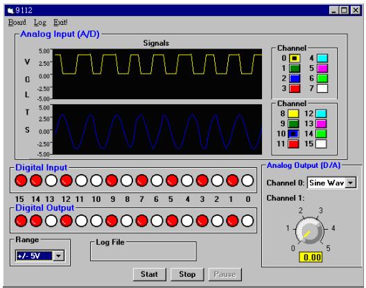
![9112\nBoard Log Roll\nAnalog Input (A/D)\nSignals\nV\nG\nL\nT\nS\n5.00\n2.50\n0.00\n-2.50\n-5.00\n2.50\n0.00\n-2.50\n-5.00\nChannel\n0 4\n1 5\n2 6\n3 7\nChannel\n8 12\n9 13\n10 14\n11 15\nDigital Input\nDigital Output\nRange\n+/- 5V\nLog File\nStart Stop Pause\nAnalog Output (D/A)\nChannel 0: Sine Wave\nChannel 1:\n0 0.00](.pcis-dask-manual-3/a0317a728457717c3e63c9ea35114de757e0e90171a3e6e87b289616f4ce04ff.jpg)

Analog Input (A/D). Shows the results of A/D conversion. You can select the input channels (allows multiple channels) and the input range (gain) you want to test.

Analog output (D/A). Shows the results of D/A conversion. You may turn the tuner to set the output voltage. You can also set the output waveform to sine or square.

D/I and D/O. Shows the results of read/write data from/to digital input/output channels. To set the output value, click the channel buttons. A red color indicates an ON channel, while a white color indicates an OFF channel.

# Data I/O Through DMA Data Transfer or Interrupt Operation

This program demonstrates the use of PCIS-DASK to operate data I/O through DMA data transfer or Interrupt operation. The program main screen is shown below.
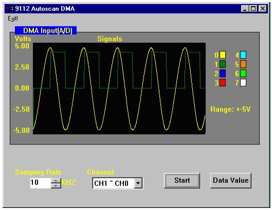
![| Channel | Value |\n| ------- | ----- |\n| 0       | 4     |\n| 1       | 5     |\n| 2       | 6     |\n| 3       | 7     |\n| Range   | +5V   |](.pcis-dask-manual-3/732517103ba1e792ee6434be50948199aebbf5849ea2796fe7b5cff3de929e75.jpg)

These programs allow you to adjust the input channels, input range (PCI-7200 does not have these two options), sampling rate, and data size (transfer count).

To view the input data, click on the Data Value button in the main screen when data transfer is finished. Refer to the following screen.
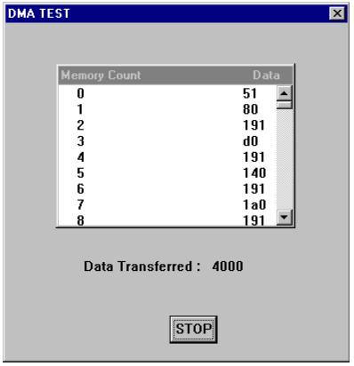
![DMA TEST\nMemory Count Data\n0 51\n1 80\n2 191\n3 d0\n4 191\n5 140\n6 191\n7 1a0\n8 191\nData Transferred : 4000\nSTOP](.pcis-dask-manual-3/16c4962e1fe2700c999ee72d1fac32fdecf1efb065220f072edf682352e117f2.jpg)

# Double Buffer Mode Data I/O Through DMA Transfer or Interrupt Operation

This program tells you how to use PCIS-DASK to operate double-buffered data I/O through DMA transfer or Interrupt operation. The program main screen is shown below:
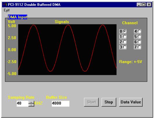
![PCI-9112 Double Buffered DMA\nExit!\nDMA Input\nVol\n5.00\nSignals\nChannel\n0 4\n1 5\n2 6\n3 7\nRange: +5V\nSampling Rate\n40 MHz\nBuffer Size\n4000\nStart Stop Data Value](.pcis-dask-manual-3/102ecf66376640279fe319a45c6fcc9dbfac9b9c47add4bf9728c5e9745a2d8f.jpg)

These programs lets you input channel, input range (PCI-7200 does not have this two options), sampling rate, and data size (transfer count).

To view the input data, click on the Data Value button in the main screen after you stop the double-buffered operation.

# Trigger Mode Data I/O Through DMA Data Transfer or Interrupt Operation

These programs tell you how to use PCIS-DASK to operate trigger mode data I/O through DMA data transfer or interrupt operation. Except for the additional input item postCount, the main screen of these programs are similar with Single-Buffer Mode or Double-Buffer Mode programs. Please refer to these two sections for the details.

The postCount item represents the number of data accessed after a specific trigger event or the counter value for deferring to access data after a specific trigger event. Refer to the description of AI configuration functions (AI\_9111\_Config, AI\_9118\_Config, AI\_9812\_Config) for details.
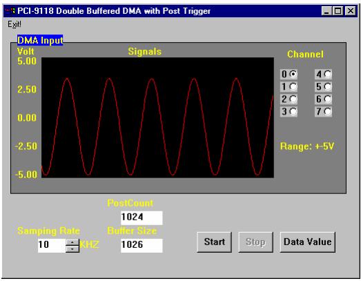
![PCI-9118 Double Buffered DMA with Post Trigger\nExit!\nDMA Input\nVol\n5.00\nSignals\nChannel\n0 4 °C\n1 °C 5 °C\n2 °C 6 °C\n3 °C 7 °C\nRange: +5V\nPostCancel\n1024\nSampling Rate\n10 1026\nBump Size\nStart Stop Data Value](.pcis-dask-manual-3/17593d85b5b137cdd2db5f4c712539820e5d6085ce1ee94c2a351e7d531a6d93.jpg)

# NOTE

Except for VB9812, all trigger mode data acquisition sample programs use external digital trigger source to provide trigger signal. Refer to the card's documentation if you want to operate for the detailed description of trigger mode data acquisition.

# 8 Distribution of Applications

# 8.1 Required Files

When installing an application that uses PCIS-DASK on another computer, you must install the necessary driver files and supporting libraries on the target system. You can create an automatic installer that installs your program and all files needed to run the program or you can install the program and program files manually. For both installation methods, you must install the following files:

# Required support DLLs: Pci-dask.dll

# Driver files

Windows® 98

Corresponding driver files in \Software\Pcisdask\W98NT2K\redist\W98\drivers (e.g. pci7200.sys for PCI-7200). These files must be copied to the Windows\system32\drivers directory.
Corresponding INF files in \Software\Pcis-dask\W98NT2K\redist\W98\Inf (e.g. p7200.inf for PCI-7200). These files must be copied to the Windows\inf directory.
▶ Device configuration utility in \Software\Pcisdask\W98NT2K\redist\W98\Util.

Windows $^{®}$ NT 4.0

- adldask.sys in \Software\Pcis-dask\W98NT2K\redist\Wnt\drivers. This file must be copied to Winnt\system32\drivers directory.
Corresponding driver files in \Software\Pcisdask\W98NT2K\redist\Wnt\drivers (e.g. pci7200.sys for PCI-7200). These files must be copied to Winnt\system32\drivers directory.
▶ Device configuration utility in \Software\Pcisdask\W98NT2K/redist\Wnt\Util.

Windows® 2000

Corresponding driver file in \Software\Pcisdask\W98NT2K\redist\W2000\drivers (e.g. pci7200.sys for PCI-7200). These files must be copied to Winnt\system32\drivers directory.

Corresponding INF file in \Software\Pcis-dask\W98NT2K\redist\W2000\Inf (e.g. p7200.inf for PCI-7200). These files must be copied to Winnt\inf directory.
▶ Device configuration utility in \Software\Pcisdask\W98NT2K\redist\W2000\Util.

# Utility file (option)

Data conversion utility DAQCvt.exe in \Software\Pcisdask\W98NT2K\redist\W98\Util, \Software\Pcisdask\W98NT2K\redist\Wnt\Util, or \Software\Pcisdask\W98NT2K\redist\W2000\Util to convert the binary data file to an easily read file format.

# 8.2 Automatic Installers

Several programming environments provide setups or distribution kit tools that automatically create an installation program so that it can be conveniently installed from one computer to another. For the application to function properly, this tool must locate and include the required control files and supporting libraries in the installation program that it creates.

Some tools, such as the Visual Basic 5 Setup Wizard, uses dependency files to determine which libraries are required by a VB application. Some setup tools may not automatically recognize which files are required by a program, but they provide an option to add additional files to the installation program. In this case, verify that all the necessary files described in the previous section are included. The user should also check if the resulting installation program does not copy older versions of a file over a newer version on the target computer.

If the programming environment does not provide a tool or wizard for building an installation program, third-party tools such as InstallShield may be used instead. Some programming environments provide simplified or trial versions of third-party installer creation tools on their installation CDs.

# 8.3 Manual Installation

If the programming environment does not include a setup or distribution kit tool, the installation task may be performed manually. To install the program to another computer:

1. Copy the program executable to the target computer.
2. Copy all required PCIS-DASK files described in the section 8.1 to the appropriate directory on the target computer.
3. Use NuDAQ Device Configuration utility to configure the device.

NOTE Do not replace a newer version of a file installed in the target computer.
[🔗 Link to the original document](.pcis-dask-manual-3/pcis-dask-manual-3.pdf)
