# PXES-2590

# 3U 9-Slot PXI Express Chassis

# User's Manual

![Front view of an ADLINK PXI5-2090 Channel industrial control unit (no visible text or symbols on the device body)](.pxes-2590-50-17038-1000-200-en-en/6d0e1e2c15c964feae23009652fd1255e43f893b7bbca6f5febf3c9742c90343.jpg)

Manual Rev.: 2.00

Revision Date: June 29, 2012

Part No: 50-17038-1000

![Circular black-and-white recycling symbol with three white arrows forming a triangle (no text or symbols)](.pxes-2590-50-17038-1000-200-en-en/2d54a945c2164e108c0315085a277764cd84ffe3a0e9ae70c0be634ef2b03fac.jpg)

Recycled Paper

# Revision History

<table><tr><td>Revision</td><td>Release Date</td><td>Description of Change(s)</td></tr><tr><td>2.00</td><td>2012/6/29</td><td>Initial Release</td></tr></table>

# Preface

# Copyright 2012 ADLINK TECHNOLOGY, INC.

This document contains proprietary information protected by copyright. All rights are reserved. No part of this manual may be reproduced by any mechanical, electronic, or other means in any form without prior written permission of the manufacturer.

# Disclaimer

The information in this document is subject to change without prior notice in order to improve reliability, design, and function and does not represent a commitment on the part of the manufacturer.

In no event will the manufacturer be liable for direct, indirect, special, incidental, or consequential damages arising out of the use or inability to use the product or documentation, even if advised of the possibility of such damages.

# Environmental Responsibility

ADLINK is committed to fulfill its social responsibility to global environmental preservation through compliance with the European Union's Restriction of Hazardous Substances (RoHS) directive and Waste Electrical and Electronic Equipment (WEEE) directive. Environmental protection is a top priority for ADLINK. We have enforced measures to ensure that our products, manufacturing processes, components, and raw materials have as little impact on the environment as possible. When products are at their end of life, our customers are encouraged to dispose of them in accordance with the product disposal and/or recovery programs prescribed by their nation or company.

# Trademarks

Product names mentioned herein are used for identification purposes only and may be trademarks and/or registered trademarks of their respective companies.

# Conventions

Take note of the following conventions used throughout this manual to make sure that users perform certain tasks and instructions properly.

![The image shows a white document icon with horizontal grey lines running across it. A large, bold red checkmark is drawn diagonally across the center of the document. The top right corner of the document is slightly curled.](.pxes-2590-50-17038-1000-200-en-en/543237c27a97b7d278009d41f1011d46d7ac02ce23614343061be27c6425a19f.jpg)
NOTE:

Additional information, aids, and tips that help users perform tasks.

![The image shows a yellow triangular warning sign with a black border. Inside the triangle is a black exclamation mark.](.pxes-2590-50-17038-1000-200-en-en/646b2952d0f67558056214f37bf25ef167523c5fd62b2a90f1fea9536e212ae0.jpg)
CAUTION:

Information to prevent minor physical injury, component damage, data loss, and/or program corruption when trying to complete a task.

![This image displays a triangular warning sign with a black outline. The interior features a red gradient, transitioning from a lighter shade at the top to a darker red at the bottom. In the center is a large white exclamation point.](.pxes-2590-50-17038-1000-200-en-en/30e8ef0941ed37b9b7c1ad8b6a380a890e293e3ae7b6c2ab6a9de7260b86db61.jpg)
WARNING:

Information to prevent serious physical injury, component damage, data loss, and/or program corruption when trying to complete a specific task.

# Table of Contents

# Revision History...... ii

# Preface .... iii

# List of Figures ...... vii

# List of Tables ix

# 1 Introduction ...... 1

1.1 Features.... 2
1.2 Specifications.... 3
1.3 Schematics 6
1.4 Connectors, I/O, and Controls 9

1.4.1 Front Panel 9
1.4.2 Rear Panel.... 10
1.4.3 Backplane.... 12

# 2 Getting Started 19

2.1 Package Contents 19
2.2 Cooling Considerations.... 20
2.3 Hardware Installation 21

2.3.1 Installing the System Controller 21
2.3.2 Installing Peripheral Modules 23
2.3.3 Powering Up the System 26

# 3 System Management.... 27

3.1 Installing the Monitor Utility 27
3.2 Monitoring the PXES-2590 27

3.2.1 Connect Control....28
3.2.2 Threshold and Control 30
3.2.3 Chassis Status.... 32

# 4 Monitoring/Control Functions 33

4.1 SMBus API.... 33
4.2 Function Overview 33
4.3 Function Library 34

# A Appendix: PMK-1524 Monitor Kit 57

A.1 Overview.... 57
A.2 Specifications.... 58
A.3 Package Contents.... 59
A.4 Installing the PMK-1524.... 60
A.5 Connecting the PMK-1524.... 65

A.5.1 Keyboard Detachment....66

A.6 Driver Installation 66
A.7 OSD Controls and Menu.... 71

A.7.1 OSD Menus 72

# B Appendix: Troubleshooting and Maintenance.... 73

B.1 Installation Problems.... 73
B.2 Basic Troubleshooting 74
B.3 Maintenance 75

B.3.1 Handling the Chassis....75
B.3.2 Cleaning the Exterior 75
B.3.3 Power Requirements 75

# Important Safety Instructions.... 77

# Getting Service 79

# List of Figures

Figure 1-1: Front View 6

Figure 1-2: Right Side View 6

Figure 1-3: Left Side View....7

Figure 1-4: Top View....7

Figure 1-5: Underside View 8

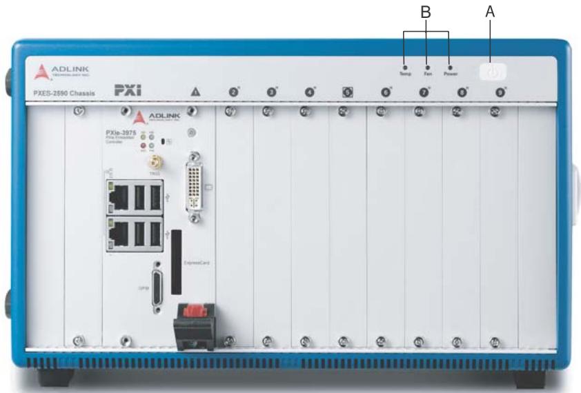
Figure 1-6: PXES-2590 Front Panel 9

Figure 1-7: PXES-2590 Rear Panel....10

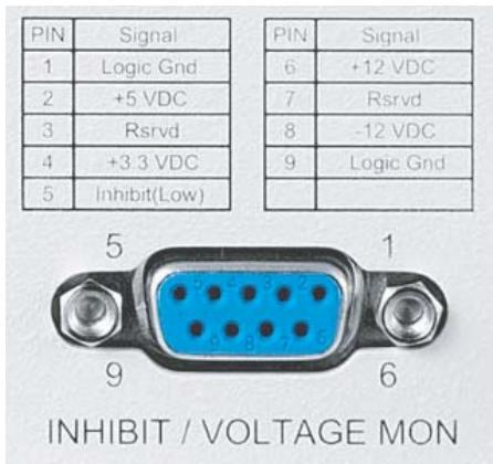
Figure 1-8: Inhibit/ Voltage Monitoring Connector .... 12

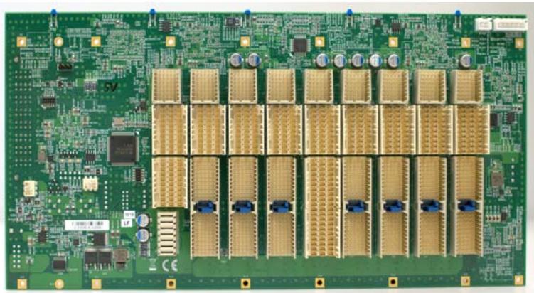
Figure 1-9: PXES-2590 Backplane 12

Figure 1-10: Single-ended Star Trigger Routing .... 13

Figure 1-11: Differential Star Trigger Routing .... 14

Figure 1-12: 3U hybrid slot compatible PXI-1 peripheral module . 15

Figure 1-13: 3U PXI Express peripheral module .... 15

Figure 1-14: PXES-2590 Backplane Indicators 17

Figure 3-1: FTP Monitor Interface....28

Figure 3-2: Target Temperature Parameters and Legend ..... 31

Figure A-1: PMK-1524....57

Figure A-2: PXES-2590 Chassis Schematic 60

Figure A-3: PMK-1524 Connection to PXES-2590....65

Figure A-4: PMK-1524 Keyboard Detachment 66

Figure A-5: Driver Installation Introduction 66

Figure A-6: Installation Start 67

Figure A-7: Interface Selection 1....68

Figure A-8: Interface Selection 1....69

Figure A-9: 4-point Calibration Setup 70

Figure A-10: OSD Controls 71

This page intentionally left blank.

# List of Tables

Table 1-1: Front Panel Legend ...... 9
Table 1-2: Front Panel Indicators.... 10
Table 1-3: Rear Panel Legend.... 11
Table 1-4: Backplane Indicator Legend 17
Table 1-5: 10MHz Reference Clock Priority.... 18
Table 3-1: Log Options Commands....29
Table 4-1: PXES-2590 Functions 34
Table A-1: PMK-1524 Legend 58
Table A-2: PXES-2590 Chassis Schematic Legend 60

This page intentionally left blank.

# 1 Introduction

The ADLINK PXES-2590 is a 9-slot PXI Express chassis with advanced features and functions. Compliant with PXI Express and cPCI Express specifications, the PXES-2590 offers one system slot, one system timing slot, and seven hybrid peripheral slots for versatile testing and measurement applications requiring enhanced bandwidth. The hybrid-slot design accepts installation of CompactPCI, PXI, CompactPCI Express, and PXI Express modules into any peripheral slot, maximizing flexibility. The PXES-2590 is built on a four-link PXI express chassis with up to 8 GB/s system bandwidth, and 1 GB/s slot bandwidth for all peripheral slots.

The PXES-2590 implements a smart system monitoring controller, reporting full chassis status, including fan speed, system voltages, and internal temperature.

Equipped with an industrial grade AC power supply, the PXES-2590 can provide 400 W in environments from 0°C to 55°C, and features an innovative cooling scheme providing superior heat dissipation. Two 185.9CFM fans in the rear section of the chassis draw cool air from apertures on the bottom and front of the chassis, over the PXI modules, and exhausted to the rear. This innovative cooling design provides, not only exceptional efficiency of heat dissipation, but also superior uniformity for each PXI slot. BNC connectors for 10 MHz clock input/output on the rear panel increase chassis flexibility, enabling synchronization with supplementary devices.

# 1.1 Features

- PXI $^{TM}$ -5 PXI Express hardware specification Rev.1.0 compliant
▶ 9-slot PXI Express chassis with one system slot, one system timing slot, and seven hybrid peripheral slots
▶ Four-link PXI Express chassis
▶ Up to 8 GB/s system bandwidth
▶ Up to 1 GB/s peripheral bandwidth for all slots
▶ 0°C to 55°C extended operating temperature range
▶ Intelligent chassis management
▶ Automatic fan speed control
▷ Chassis status monitoring and reporting
▶ Remote chassis power on/off control
▶ BNC connectors for 10 MHz clock input/output
▶ 400 W industrial-grade AC power supply
▶ Power, temperature, and fan monitoring LEDs

# 1.2 Specifications

The PXES-2590 complies with the PXI $^{TM}$ -5 Specification Rev.1.0 and accepts all modules compliant with the PXI $^{TM}$ -5 and Compact PCI specification.

<table><tr><td colspan="4">General Specifications</td></tr><tr><td colspan="4">Power Supply</td></tr><tr><td colspan="4">AC Input (*guaranteed by power supply design)</td></tr><tr><td colspan="2">Input voltage range</td><td colspan="2">100 to 240 VAC</td></tr><tr><td colspan="2">Operating voltage range*</td><td colspan="2">85 to 264 VAC</td></tr><tr><td colspan="2">Input voltage frequency</td><td colspan="2">50 to 60 Hz</td></tr><tr><td colspan="2">Operating voltage frequency*</td><td colspan="2">47 to 63 Hz</td></tr><tr><td colspan="4">Input current rating</td></tr><tr><td colspan="2">115 VAC</td><td colspan="2">13 A</td></tr><tr><td colspan="2">230 VAC</td><td colspan="2">10 A</td></tr><tr><td colspan="4">DC Output</td></tr><tr><td colspan="2">Maximum total usable power</td><td colspan="2">400 W</td></tr><tr><td>VDC</td><td>Maximum</td><td>Load Regulation</td><td>Maximum Ripple &amp; Noise</td></tr><tr><td>+5V</td><td>23.0 A</td><td>±3%</td><td>50 mV</td></tr><tr><td>+12V system slot</td><td>15.0 A</td><td>±3%</td><td>50 mV</td></tr><tr><td>+12V peripheral slots</td><td>16.0 A</td><td>±3%</td><td>50 mV</td></tr><tr><td>+3.3V</td><td>33.0 A</td><td>±3%</td><td>50 mV</td></tr><tr><td>-12V</td><td>1.75 A</td><td>±3%</td><td>50 mV</td></tr><tr><td colspan="4">10 MHz System Reference Clock (10 MHz REF)</td></tr><tr><td colspan="2">Maximum clock skew between slots</td><td colspan="2">300 ps</td></tr><tr><td colspan="2">Built-in 10 MHz clock Accuracy</td><td colspan="2">±50 ppm</td></tr><tr><td colspan="2">BNC Output amplitude</td><td colspan="2">1 Vpk-pk ±20% square-wave into50 Ω2 Vpk-pk unloaded</td></tr><tr><td colspan="2">BNC Output impedance</td><td colspan="2">50 Ω ±5 Ω</td></tr><tr><td colspan="4">External 10 MHz clock source input requirements</td></tr><tr><td colspan="2">Frequency input</td><td colspan="2">10 MHz ±100 PPM</td></tr></table>

<table><tr><td colspan="2">General Specifications</td></tr><tr><td>Input signal (10MHz REF In BNC)</td><td>100 mVPP to 5 VPP(square or sine)</td></tr><tr><td>Input impedance (10MHz REF In BNC)</td><td>50 Ω ±5 Ω</td></tr><tr><td>Input signal (PXI_CLK10_IN on fifth slot)</td><td>5 V or 3.3 V TTL signal</td></tr><tr><td colspan="2">100 MHz System Reference Clock: PXle_CLK100</td></tr><tr><td>Maximum slot-to-slot skew</td><td>100 ps</td></tr><tr><td>Accuracy</td><td>±25 ppm</td></tr><tr><td colspan="2">Cooling</td></tr><tr><td>Fans</td><td>2 sets of 185.9 CFM fans</td></tr><tr><td>Per-slot cooling capacity</td><td>30 W (verified by 55°C chamber test)</td></tr><tr><td colspan="2">Physical</td></tr><tr><td>Slots</td><td>9(1 x system slot, 1 x system timing slot, 7 x hybrid peripheral slots)</td></tr><tr><td>Dimensions</td><td>321.9 (W) x 191.4 (H) x 465.3 (D) mm (12.7 x 7.5 x 18 in.)</td></tr><tr><td>Weight</td><td>8.8 kg (19.4 lb)</td></tr><tr><td colspan="2">Environmental</td></tr><tr><td>Storage</td><td>Ambient temperature: -20 to 70°CRelative humidity: 10 to 90%, noncondensing</td></tr><tr><td>Operating</td><td>Ambient temperature: 0 to 55°CRelative humidity10 to 90%, noncondensing</td></tr><tr><td>Functional shock</td><td>30 G, half-sine, 11 ms pulse duration</td></tr><tr><td>Random Vibration</td><td>Operating: 5 to 500 Hz, 0.31 Grms, 3 axesNonoperating: 5 to 500 Hz, 2.46 Grms, 3 axes</td></tr><tr><td colspan="2">Certification</td></tr><tr><td>Safety</td><td>EN 61010-1</td></tr><tr><td>Electromagnetic Compatibility</td><td>Emissions: EN 55011 Class A Immunity: EN 61326-1</td></tr><tr><td>CE Compliance</td><td>Meets essential requirements of applicable European Directives, as amended for CE Marking:Low-Voltage Directive (safety): 73/23/EEC Electromagnetic Compatibility Directive (EMC): 9/336/EEC</td></tr></table>

# 1.3 Schematics

![The image displays a standard warning sign featuring a red triangle with a white exclamation point in the center. Below the triangle is a white rectangle containing the word 'WARNING' in black capital letters.](.pxes-2590-50-17038-1000-200-en-en/c1ce5e80474afdeec11de9e3e7e21cd9985c25a587f1126f80bab8ebac76e802.jpg)

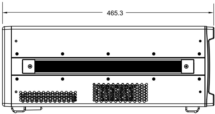
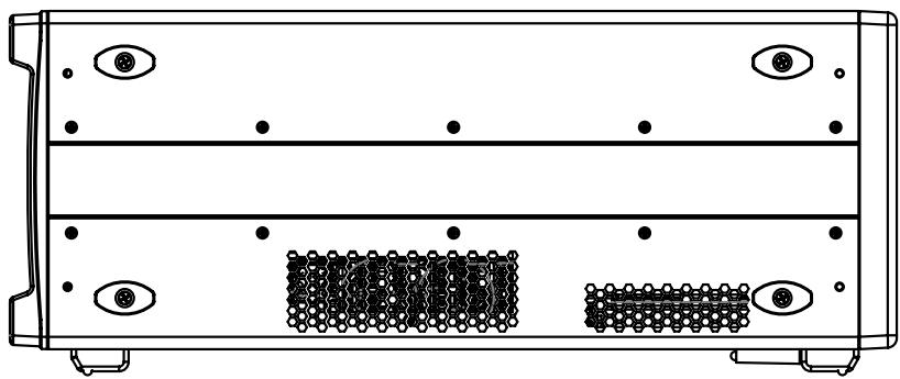
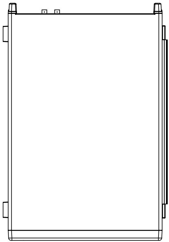
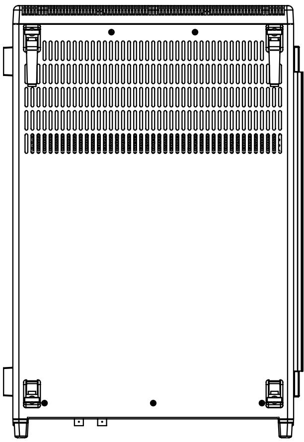
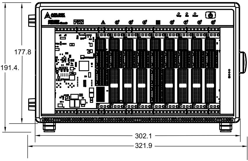
Please note that all dimensions are shown in mm (millimeters)
![177.8\n191.4.\n302.1\n321.9](.pxes-2590-50-17038-1000-200-en-en/108509ae3f914a86a5f366a98b80543a2b22132334c56e49bd6b638b3be1e8d2.jpg)

Figure 1-1: Front View
![465.3](.pxes-2590-50-17038-1000-200-en-en/06ea811524e546bdc291287426201d13c36b17f398e009cb4c1352b3d2fb79ba.jpg)

Figure 1-2: Right Side View

![Technical line drawing of a server rack with two rows of circular components and mounting holes (no text or symbols)](.pxes-2590-50-17038-1000-200-en-en/b609e20c49044d78fa880003fe11f8470acc49e2a55cc691449379e2dda14f12.jpg)

Figure 1-3: Left Side View

![Pure technical line drawing of a rectangular frame with corner brackets and mounting holes (no text or symbols)](.pxes-2590-50-17038-1000-200-en-en/69605550c00d0a75c4dc30525603c921547dec91ed304d346f7090903761cdd7.jpg)

Figure 1-4: Top View

![Front view of a server rack unit with cooling fins and mounting feet (no text or symbols)](.pxes-2590-50-17038-1000-200-en-en/f5e410668b2ce69cca336998a2992ec870cf49f353ff9a5ec285d26f8346b4e1.jpg)

Figure 1-5: Underside View

# 1.4 Connectors, I/O, and Controls

# 1.4.1 Front Panel
![ADLINK\nPXES-2590 Chassis\nB\nA\nTemp\nFan\nPower\n3*\n3*\n4*\n5*\n7*\n8*\n9*\nADLINK\nPXEp-25975\nFXI Chassis\nCopper\nTIN13\nExpressCard\nUSB](.pxes-2590-50-17038-1000-200-en-en/2194f94051c0f42767e4e036fbeb1d78e93c724049804107fdd1d156bf07dc60.jpg)

Figure 1-6: PXES-2590 Front Panel

<table><tr><td></td><td>Feature</td><td>Details</td></tr><tr><td>A</td><td>Power</td><td>Powers the chassis on/off (when INHIBIT on rear panel (not shown) is set to “DEF”)</td></tr><tr><td>B</td><td>Chassis Status</td><td>Temperature, Fan, and Power (L to R), functions as follows</td></tr></table>

Table 1-1: Front Panel Legend

<table><tr><td>Status</td><td>Temperature (Amber)</td><td>Fan (Green)</td><td>Power (Blue)</td></tr><tr><td>On (Lit)</td><td>N/A</td><td>Fans operating normally</td><td>DC voltage supply is normal</td></tr><tr><td>Off</td><td>Temperature is normal</td><td>Chassis is powered down</td><td>Chassis is powered down</td></tr><tr><td>Blinking</td><td>One or more temperature sensors exceeds threshold temperature (default 70°C)</td><td>One or more fans falls below threshold speed (default is 800RPM)</td><td>One or more power rails exceeds threshold settings (defaults are ±5% for 5V, 3.3V, +12V, and -12V)</td></tr></table>

Table 1-2: Front Panel Indicators

# 1.4.2 Rear Panel

![WARNING\nLINE RATING\nG F E D C B A\nHIGH AUTO DEF MAN INHIBIT VOLTAGE MON OUT IN](.pxes-2590-50-17038-1000-200-en-en/4b6e8e3e7fec3b21b9ab1990eb8b04ce7c07809e45f30d903dcb810785544e3e.jpg)

Figure 1-7: PXES-2590 Rear Panel

<table><tr><td></td><td>Feature</td><td>Details</td></tr><tr><td>A</td><td>10MHz Reference Clock Input</td><td>The BNC connector acts as a 10MHz reference clock input, whereby the backplane 10MHz clock is overridden in the presence of an external 10MHz clock</td></tr><tr><td>B</td><td>10MHz Reference Clock Output</td><td>The BNC connector acts as 10MHz reference clock output</td></tr><tr><td>C</td><td>Inhibit/Voltage Monitoring DB-9 Connector</td><td>The DB-9 connector monitors the four main voltage rails via digital multimeter ► voltage rail pin assignments shown in Figure 1-8 ► current limiting resistors on each voltage rail prevent accidental overload ► one Inhibit (active low) pin is provided to power the chassis on/off when the Inhibit Switch is in the MAN (manual) position, such that chassis is powered on when Inhibit pin is logic high or open, and off when Inhibit pin is grounded</td></tr><tr><td>D</td><td>Inhibit Switch</td><td>In the DEF (default) position, the front panel power button turns the power supply on/off, and in the MAN (manual) position, the INHIBIT pin on the DB-9 connector turns the power supply on/off</td></tr><tr><td>E</td><td>Fan Switch</td><td>In the HIGH position, fans operate at maximum speed, and in AUTO, the fans run based on the monitored chassis temperature</td></tr><tr><td>F</td><td>Universal Power Inlet</td><td>Accepts C13 power outlet-equipped connection</td></tr><tr><td>G</td><td>Chassis Ground Lug</td><td>The ground wire can be crimped to the ground lug, using a crimp tool of the appropriate size, with the other end connected to ground</td></tr></table>

Table 1-3: Rear Panel Legend

![PIN\n1\n2\n3\n4\n5\nSignal\nLogic Gnd\n+5 VDC\nRsrvd\n+3 3 VDC\nInhibit(Low)\nPIN\n6\n7\n8\n9\nLogic Gnd\nSignal\n+12 VDC\nRsrvd\n-12 VDC\nLogic Gnd\nINHIBIT / VOLTAGE MON](.pxes-2590-50-17038-1000-200-en-en/548dfe8bee8e6c1de86338067a2dcc75bddff683361ab0bb14dc532f7c2719f5.jpg)

Figure 1-8: Inhibit/ Voltage Monitoring Connector

# 1.4.3 Backplane
![Green printed circuit board with gold bonding pads and connectors (no visible text or symbols)](.pxes-2590-50-17038-1000-200-en-en/2b145c61d746646535e039f00c7b9cb2cf02687f8b981b5acefd165815a65a04.jpg)

Figure 1-9: PXES-2590 Backplane

# PXI Express System Controller Slot

The System Controller slot is Slot 1 of the chassis as defined by the PXI specification. The PXES-2590 chassis can accommodate a PXI Express system controller that occupies width up to 4 slots. As defined in the PXI specification, three controller expansion slots allow the controller to expand to the left to prevent the controller from using up peripheral slots.

# PXI Express System Timing Slot

The System Timing (ST) slot is Slot 5, providing one dedicated single-ended star trigger and 3 pairs of differential star trigger lines to each peripheral slot. Routing of single ended star trigger signals (PXI\_STAR) is as follows
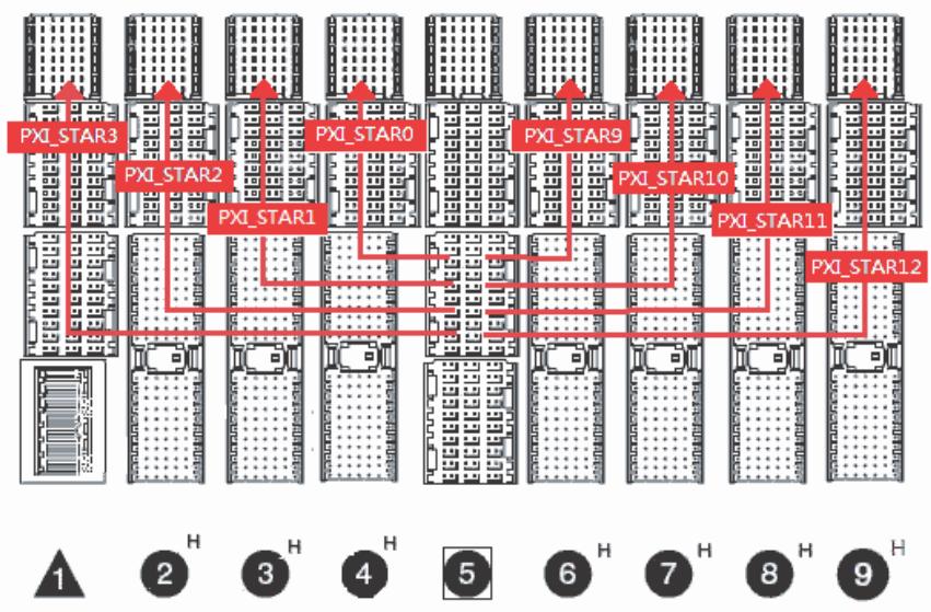
![PXI_STAR3\nPXI_STAR2\nPXI_STAR0\nPXI_STAR9\nPXI_STAR10\nPXI_STAR11\nPXI_STAR12\n1 H 2 H 3 H 4 H 5 H 6 H 7 H 8 H 9 H](.pxes-2590-50-17038-1000-200-en-en/e80ac122b5bcd0c58e6383013c9329bf63e513542d13706e7af0a1bbc6ecaef7.jpg)

Figure 1-10: Single-ended Star Trigger Routing

Routing of differential star trigger signals (PXle\_DSTAR) is as follows.
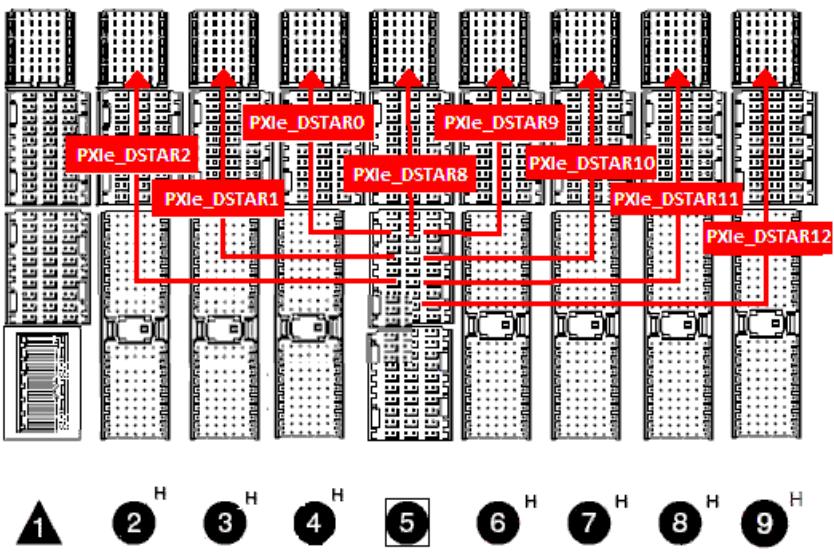
![Based on the provided flowchart/block diagram, here are the labeled blocks and their connections:\n\n**Labeled Blocks:**\n*   PXIe_DSTAR2\n*   PXIe_DSTAR0\n*   PXIe_DSTAR1\n*   PXIe_DSTAR8\n*   PXIe_DSTAR9\n*   PXIe_DSTAR10\n*   PXIe_DSTAR11\n*   PXIe_DSTAR12\n\n**Connections:**\nThe diagram displays red lines indicating signal paths that originate from the bottom section of the second vertical column (slot) and route upwards to the top section of various columns.\n*   **PXIe_DSTAR2**: A connection line originates from the bottom of the second column and points upward to the top of the second column.\n*   **PXIe_DSTAR1**: A connection line originates from the bottom of the second column and points upward to the top of the third column.\n*   **PXIe_DSTAR0**: A connection line originates from the bottom of the second column and points upward to the top of the fourth column.\n*   **PXIe_DSTAR8**: A connection line originates from the bottom of the second column and points upward to the top of the fifth column.\n*   **PXIe_DSTAR9**: A connection line originates from the bottom of the second column and points upward to the top of the sixth column.\n*   **PXIe_DSTAR10**: A connection line originates from the bottom of the second column and points upward to the top of the seventh column.\n*   **PXIe_DSTAR11**: A connection line originates from the bottom of the second column and points upward to the top of the eighth column.\n*   **PXIe_DSTAR12**: A connection line originates from the bottom of the second column and points upward to the top of the ninth column.](.pxes-2590-50-17038-1000-200-en-en/2a932f75ba8af1c2e9663b0409ead33f977c3be310354f5e5d3f6511ea258dab.jpg)

Figure 1-11: Differential Star Trigger Routing

Star trigger functionality provides a precise trigger signal to the peripheral modules by installation of a specific star trigger controller module in the ST slot. The star trigger slot can also be used as a general PXI Express peripheral slot if star trigger functionality is not required.

# PXI Express Hybrid Slots

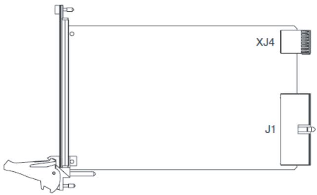
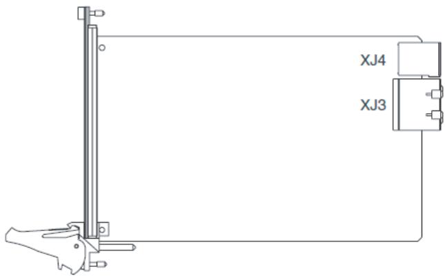
7 peripheral slots are provided in the PXES-2590, all of which are PXI Express hybrid slots. Each can accommodate a 3U PXI Express/CompactPCI Express/ hybrid slot compatible PXI-1/CompactPCI peripheral module.
![XJ4\nJ1](.pxes-2590-50-17038-1000-200-en-en/b029caad9142544b7bf045cad68182adc12f4c822c71a0ade370ee7ee6168616.jpg)

Figure 1-12: 3U hybrid slot compatible PXI-1 peripheral module
![XJ4\nXJ3](.pxes-2590-50-17038-1000-200-en-en/7c926b232c3b8d3871fa099516157e1c61657277e607a32d53113c106dd83a96.jpg)

Figure 1-13: 3U PXI Express peripheral module

# Local Bus

The local bus on a PXI backplane is a daisy-chained bus that connects each peripheral slot with adjacent peripheral slots to the left and right. The quantity of local bus lines is decreased from thirteen to one on a PXI Express backplane. The remaining local bus line can transmit analog or digital signals between modules.

# Trigger Bus

The trigger bus is an 8-line bus that connects all slots on the PXES-2590, providing inter-module synchronization. PXI and PXI Express modules can exchange trigger or clock signals through the trigger bus, allowing precisely timed response to asynchronous external events the system is monitoring or controlling.

# Reference Clock

The PXES-2590 backplane supplies single-ended 10MHz reference clock (PXI\_CLK10) and differential 100MHz clock (PXIe\_CLK100) to each peripheral slot for inter-module synchronization. The independent buffers drive the clock signal to each peripheral slot.

These common reference clock signals can synchronize multiple modules in a PXI Express chassis. PXI modules with phase-lock loop circuits can lock reference clocks to generate an in-phase timebase.

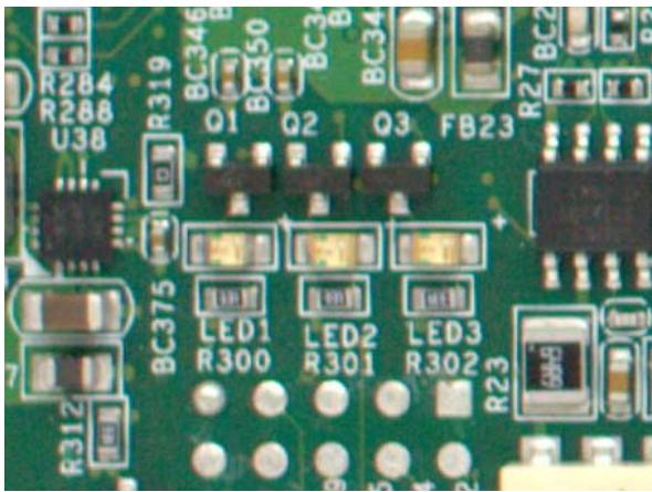
The PXI\_CLK10 and PXIe\_CLK100 clocks are in-phase according to the PXI-5 specification. Since the external 10MHz clock input can override the onboard 10MHz clock source, a phase-lock loop (PLL) circuit on the backplane synchronizes the PXIe\_CLK100 and external 10MHz clock. Three LED indicators on the left side of the system controller slot indicate status as follows.
![Close-up of a green printed circuit board with various electronic components and connectors (no readable text or symbols)](.pxes-2590-50-17038-1000-200-en-en/3ec263a0cff7229795e3b7efd67cefe7bcdb922dd705f0e727da5d1d15beb782.jpg)

Figure 1-14: PXES-2590 Backplane Indicators

<table><tr><td>Left LED (LED 1), VCXO present</td><td>Middle LED (LED 2), external clock present</td><td>Right LED (LED 3), phase-lock complete</td></tr><tr><td>Lights when the onboard VCXO is operating, should be lit at all times</td><td>Lights when external 10MHz clock is present, including from BCN connector on rear panel and from system timing slot</td><td>Lights when the external 10MHz clock is phase locked by PLL circuit</td></tr></table>

Table 1-4: Backplane Indicator Legend

The PXES-2590 PXI chassis automatically selects the 10 MHz reference clock source from

▶ Built-in accurate 10 MHz clock source
▷ External 10 MHz clock through a BNC connector
▷ PXI\_CLK10\_IN pin on the system timing slot

Priority of 10MHz reference clock is as follows

<table><tr><td>System Timing Slot (5th slot)</td><td>BNC connector on rear panel</td><td>10MHz clock driven to peripheral slots</td></tr><tr><td>No clock present</td><td>No clock present</td><td>10MHz clock is generated by backplane.</td></tr><tr><td>No clock present</td><td>10MHz clock present</td><td>Clock from BNC connector is driven to all peripheral slots</td></tr><tr><td>10MHz clock present</td><td>No clock present</td><td>Clock from system timing slot is driven to all peripheral slots</td></tr><tr><td>10MHz clock present</td><td>10MHz clock present</td><td>Clock from system timing slot is driven to all peripheral slots</td></tr></table>

Table 1-5: 10MHz Reference Clock Priority

# 2 Getting Started

This chapter describes procedures for installing the PXES-2590 and making preparations for its operation. Please contact ADLINK or authorized dealer if there are any problems during the installation.

![The image displays a white document icon with a folded top-left corner and faint horizontal lines. A large, bold red checkmark is superimposed over the center of the document.](.pxes-2590-50-17038-1000-200-en-en/435a4f63d0f4f36c7d65568db388ef304e63b8f25ae77c0be1eb0e88ec4fd8d4.jpg)
NOTE:

Diagrams and illustrated equipment are for reference only. Actual system configuration and specifications may vary.

# 2.1 Package Contents

Before unpacking, check the shipping carton for any damage. If the shipping carton and/or contents are damaged, inform your dealer immediately. Retain the shipping carton and packing materials for inspection. Obtain authorization from your dealer before returning any product to ADLINK.

Please ensure that the following items are included in the package.

▶ PXES-2590 Chassis
▶ Power cords
▶ Filler panel kit for unused/reserved slots including one 3-slot panel and nine 1-slot panels
▶ ADLINK All-in-One CD
▶ User's Manual

If any of these items are missing or damaged, contact the dealer from whom you purchased the product. Save the shipping materials and carton in case you want to ship or store the product in the future.

![The image shows a standard safety symbol featuring an upward-pointing triangle with a red gradient background that transitions from light red at the top to dark red at the bottom. Inside the triangle is a large white exclamation point. Below the triangle, the word 'WARNING' is printed in bold, black capital letters.](.pxes-2590-50-17038-1000-200-en-en/6a268fbb997d7076bd2c31bc2caabf43ea1f8b18dcfc65a4bd9a4a9328302ea8.jpg)

Do not install or apply power to equipment that is damaged or missing components. Retain the shipping carton and packing materials for inspection. Please contact your ADLINK dealer/vendor immediately for assistance and obtain authorization before returning any product.

# 2.2 Cooling Considerations

The PXES-2590 features an innovative design for heat dissipation, with cooling fans in the rear section of the chassis, drawing cool air through apertures on the bottom for exhaust through the back. This design provides uniform airflow for each PXI slot and exceptional cooling capability. When the chassis is installed in a rack, the cooling design minimizes drawing of hot air from the rear area, where other devices exhaust, while maintaining a steady temperature inside the chassis. For optimal cooling efficiency, retain support feet.

When rack mounting the PXES-2590, at least 1U (44.5 mm/1.75 in.) clearance below the intake apertures is required. Also keep other objects or equipment at a minimum of 76.2 mm (3 in.) away from the outlet apertures in the rear region of the chassis.

![The image displays a white document icon with a folded top-left corner and faint horizontal lines running across it. A large, bold red checkmark is superimposed over the document, angling upwards from the bottom left to the top right.](.pxes-2590-50-17038-1000-200-en-en/a219a86fa1a3b8327af0fc5783ccd0a344b02d160941c85614ec7bfa148bc6ee.jpg)
NOTE:

To maintain expected air flow, always install filler panels in unused slots. The filler panels can be found in the chassis package.

# 2.3 Hardware Installation

# 2.3.1 Installing the System Controller

The PXES-2590 incorporates a system controller slot supporting a PXI Express system controller of 3 or 4 slot width. We recommend the ADLINK PXIe-3975 Core™ i5-520E Controller for use with the PXES-2590.

1. Ensure the CPU, memory module(s), and storage device(s) are properly installed on the system controller.
2. Locate the system controller slot (Slot 1).

![Front view of an A2LINK FXI oscilloscope module with a red circle highlighting a component, no visible text or symbols on the device itself.](.pxes-2590-50-17038-1000-200-en-en/7399dd805a761a15fc42a550d321ca44aebaf04bf5f851ea9d08d9249c30e6ef.jpg)

3. Depress the system controller module's latch to release.

4. Align the module's top and bottom edges with the card guides, and carefully slide the module into the chassis.

![Front view of an electronic device labeled 'FXI' with visible internal components and a red arrow pointing to a component (no readable text or symbols beyond labels)](.pxes-2590-50-17038-1000-200-en-en/bcf7655cf5fa91e7bd27bb4a64bc41037a16b02ed8d00983dda287d5e368777c.jpg)

5. Lift the latch until the module is securely seated in the chassis backplane.

![Front view of an ADLINK PXI oscilloscope module with visible ports and a red arrow pointing to the internal components (no readable text or symbols on the device itself)](.pxes-2590-50-17038-1000-200-en-en/ab36d58c967a8dc0aab5076f30990dcca3993b10df64970b9c34bfe578b9e7b9.jpg)

6. Fasten the screws on the module front panel, and connect all devices to the system controller.

![ADLINK\nFXI\nFXI 2000\nFXI 2000\nFXI 2000\nFXI 2000\nFXI 2000\nFXI 2000\nFXI 2000\nFXI 2000\nFXI 2000\nFXI 2000\nFXI 2000\nFXI 2000\nFXI 2000\nFXI](.pxes-2590-50-17038-1000-200-en-en/9ee925cf148d098075d4272b0ac80b33afe09145a889d27b4f9bd18e3c44f8f1.jpg)

# 2.3.2 Installing Peripheral Modules

The PXE-2590 supports up to eight peripheral modules, including a system timing module.

1. Select an available peripheral slot (2 to 9)
2. Depress the peripheral module's latch and align the module's top and bottom edges with the card guides.

3. Carefully slide the module into the chassis.

![Close-up of an ADLINK 2.500 Pkt Chassis FXI device showing internal circuit board and ports (no readable text or symbols)](.pxes-2590-50-17038-1000-200-en-en/a67ad930f53ad61ca3c5aafaf32ff754936a534c1fb8cfea4b0a702396308295.jpg)

4. Lift the latch until the module is securely seated in the chassis backplane.

![ADLINK\nFXI\n2.54 Micro Channel\nFXI\nADLINK\nFXI-254\nFXI-254\nFXI-254\nFXI-254\nFXI-254\nFXI-254\nFXI-254\nFXI-254\nFXI-254\nFXI-254\nFXI-254\nFXI-254\nFXI-254\nFXI-254\nFXI-254\nFEN-254\nFXI-254\nFXI-254\nFXI-254\nFXI-254\nFXI-254\nFXI-254\nFXI-254\nFXI-254\nFXI-254\nFXI-254\nFXI-254\nFXI-254\nFXI-254\nFXI-197\nFXI-197\nFXI-197\nFXI-197\nFXI-197\nFXI-197\nFXI-197\nFXI-197\nFXI-197\nFXI-197\nFXI-197\nFXI-197\nFXI-197\nFXI-197\nFXI-197\nFEN-254\nFXI-254\nFXI-254\nFXI-254\nFXI-254\nFXI-254\nFXI-254\nFXI-254\nFXI-254\nFXI-254\nFXI-254\nFXI-254\nFXI-254\nFXI-254\nFEN-197\nFXI-197\nFXI-197\nFXI-197\nFXI-197\nFXI-197\nFXI-197\nFXI-197\nFXI-197\nFXI-197\nFXI-197\nFXI-197\nFXI-197](.pxes-2590-50-17038-1000-200-en-en/707c3c2f6aa8cf043464999d5ed57f439059dce8e5c14e4f6cd63cbf4c860fe7.jpg)

# 5. Fasten the screws on the module's front panel.

![Close-up of an electronic device labeled PXI with a red circle highlighting a component, showing ports and connectors (no readable text beyond branding)](.pxes-2590-50-17038-1000-200-en-en/8dd3c1932777c18622ba5b7af22522f4861a7c7dd2896e987b035a473d6efb73.jpg)

# 6. Repeat steps 1 to 5 to install additional PXI peripheral modules.

![The image shows a graphic icon of a white document with a folded top-right corner. Faint horizontal grey lines run across the page. A large, thick red checkmark is superimposed over the center of the document.](.pxes-2590-50-17038-1000-200-en-en/f8c16bde7c940f843ae7d40eee4c4f6cbf18c17e4001dfbbf2cc5345d3bc0d2c.jpg)
NOTE:

To improve efficiency of heat dissipation, after installing all PXI modules, please install filler plates for any unused slots.

# 2.3.3 Powering Up the System

The PXES-2590 is equipped with a 100 VAC to 240 VAC universal power supply unit requiring no input voltage selection.

1. Connect one end of the supplied power cord to the power inlet located at the rear side of the chassis.
2. Plug the other end of the AC power cord to a properly grounded wall socket or power strip.
3. Press the standby power switch. The Power LED (blue) lights up immediately
4. To power off the chassis, press the standby power switch.

# 3 System Management

The PXES-2590 chassis provides advanced system monitoring and control. Chassis conditions, including internal temperature, fan speed, and DC voltage, are exported via SMBus, allowing detailed chassis status to be monitored on the system controller.

# 3.1 Installing the Monitor Utility

![The image displays a standard yellow triangular warning sign with a black exclamation mark in the center. Below the triangle, the word 'CAUTION:' is written in black, uppercase letters.](.pxes-2590-50-17038-1000-200-en-en/c2e049c2fe1ca3c2c198a75ba9b979b7bdcfebc77bfed8c279b00c6b76f88a96.jpg)

The FTP monitor utility can only be used with an ADLINK PXI Express controller. A customized utility is required for use with a 3rd party embedded controller. Please see Section 4.3: Function Library if development of a customized utility is desired.

The remote monitoring utility and function library are provided on the ADLINK All-in-One CD.

To install the monitoring utility:

1. Connect a USB CD-/DVD-ROM drive to the system controller.
2. Place the ADLINK All-in-Once CD in the drive.
3. Locate the monitoring utility in the folder
X:\Driver Installation\PXI Platform\PXI chassis\PXES-2590\FTP Monitor\_PXES2590\_V1.7.exe\
(where X: denotes the CD-ROM drive)
4. Double-click FTP Monitor\_PXES2590\_V1.7.exe to begin installation.

# 3.2 Monitoring the PXES-2590

ADLINK provides a GUI program:

(FTP Monitor\_PXES2590\_V1.7.exe)

to monitor the status of the PXES-2590.

As shown, the utility is divided into three interface categories: Connect Control, Threshold & Control, and Chassis Status.

![FTP Monitor V1.7 for PXES-2590\nChassis Status\nDC Voltage (V)\n5Vsb 4.982 Normal\n3.3V 3.288 Normal\n5V 4.982 Normal\n12V 11.956 Normal\n-12V -11.928 Normal\nChassis Temperature (°C)\nT1 23.8 Normal\nT2 26.3 Normal\nT3 23.9 Normal\nT4 24.4 Normal\nT5 25.0 Normal\nFan Speed (RPM)\nF1 1811 Normal\nF2 1889 Normal\nThreshold and Control\nTarget Temperature (°C)\n50 Target Temperature\nFan Speed Control\nAuto Auto Full\nAlarm Threshold DC Voltage (V)\nHigh Threshold Low Threshold\n5Vsb 5.250 5.0% 4.750 5.0%\n3.3V 3.465 5.0% 3.135 5.0%\n5V 5.250 5.0% 4.750 5.0%\n12V 12.600 5.0% 11.400 5.0%\n-12V -11.400 5.0% -12.600 5.0%\nPower Threshold\nAlarm Threshold Temperature (°C)\n70 Temp Threshold\nAlarm Threshold Fan (RPM)\n800 Fan Threshold\nConnect Control\nStart Stop\nChassis Status Log\nLog Chassis Status\nOver Threshold Statistics\nThreshold Settings\nSave Threshold Settings\nLoad Threshold Settings\nLoad Default Threshold\nVersion Info\nFPGA Ver.: BB28-1156 (2011/11/28 11:6)\nFPGA CLK: 1: Internal\nMCU V1.8\nGet Chassis Data! Count=1](.pxes-2590-50-17038-1000-200-en-en/dad8136c8fa60c5274c6c0db0f9345f12c80f88d3d8c0518278f032e3d778f32.jpg)

Figure 3-1: FTP Monitor Interface

# 3.2.1 Connect Control

# Start/Stop Monitoring

Selecting Start initializes monitoring, and selecting Stop ends the operation.

# Chassis Status Log

With the Chassis Status Log function, monitored data can be recorded. Clicking Log Chassis Status opens the Log Options dialog, as shown.

![Dialog: Log Options!\nLog File\nLog.txt\nBrowse\nOption\nOverwrite the File\nAppend To File\nLog Period\nLog Period: 10 Seconds\nStart Cancel](.pxes-2590-50-17038-1000-200-en-en/5f9132cce74e438f97c9818563d0299d48c1b366ba94fe11ae3ecd59e230c66d.jpg)

<table><tr><td>Command</td><td>Details</td></tr><tr><td>Log File</td><td>Path and name for log file.</td></tr><tr><td>Option</td><td>When a log file exists and logging commences, replaces (overwrites) the current file or appends new data into the file.</td></tr><tr><td>Log Period</td><td>Interval between data logging.</td></tr></table>

Table 3-1: Log Options Commands

# Over Threshold Statistics

When selected, displays over threshold statistics.

# Save/Load Threshold

All Threshold & Control settings can be saved or loaded here. Clicking Save Threshold Settings saves all current settings. Clicking Load Threshold Settings loads all settings from the saved file. Clicking Load Default Threshold resets all threshold settings to the default values.

# Version Info

Displays the current firmware version and 10MHz clock source.

# 3.2.2 Threshold and Control

Provides operational and threshold settings for the PXES-2590, including target temperature, fan mode, and threshold settings for DC voltage, temperature, and cooling fan speeds.

# Target Temperature

Fans run at different speeds based on the monitored temperature, when the Fan switch on the rear panel is set to AUTO. Target Temp indicates the temperature when the fans are at 100%. Using the default 50°C as an example, fans run at 40% when all temperature readings are less than 25°C, and begin rampup when any reading exceeds 25°C. The fans run 100% speed if any temperature reading exceeds 50°C (Target Temperature). Target temperature setting parameters are as shown.

![| Fan voltage duty cycle (%) | Value |\n| -------------------------- | ----- |\n| 40                         | 40    |\n| 100                        | 100   |](.pxes-2590-50-17038-1000-200-en-en/ce6f98ecc93971615d5cd99e772d31607c880a588b1ad73bad0792e0d6b8e521.jpg)

Highest temperature (°C) reported by the 8 backplane sensors

<table><tr><td></td><td>Temperature</td><td>Event</td></tr><tr><td>A</td><td>0°C</td><td>Lowest chassis temperature at which fan speeds commence ramping up for final 25° temperature mark (see Item E)</td></tr><tr><td>B</td><td>45°</td><td>Highest chassis temperature at which fan speeds commence ramping up for final 70° temperature mark (see Item C)</td></tr><tr><td>C</td><td>70°</td><td>Highest maximum chassis temperature at which the fans reach maximum speed</td></tr><tr><td>D</td><td>25°C to 70°C (45 degree range)</td><td>Range over which maximum chassis temperature (at which fans reach maximum speed) can be set</td></tr><tr><td>E</td><td>25°C</td><td>Lowest maximum chassis temperature at which fans reach maximum speed</td></tr></table>

Figure 3-2: Target Temperature Parameters and Legend

Target Temp can be set by entering the desired target temperature value in the field and clicking Set.

# Fan Speed

Auto/Full status of the PXES-2590 is shown here, Auto is displayed when the cooling fans are set to auto mode and Full when the fans are set to run full speed. Selection of Auto or Full values and clicking Set directly changes cooling fan mode.

# Alarm Threshold

Active alarm threshold settings are shown, including DC voltage, temperature, and fan speeds. The updated threshold setting can also be set here, by entering the desired value and clicking Set Threshold Settings.

# 3.2.3 Chassis Status

# DC Voltage

The monitored 5V AUX, 3.3V, 5V, 12V, and -12V power rail readings are shown here. The status shows as normal when the readings are within the threshold range, and abnormal when the readings exceed the threshold range.

# Chassis Temperature

Temperature sensors T1 to T5 located on the backplane from left to right provide status, showing as normal when under the threshold value ( $70^{\circ}$ C in the figure), and abnormal when exceeding the threshold value.

# Fan Speed

Monitored readings of the three cooling fans appear here. Status shows as normal when readings exceed threshold value (800 RPM in the figure), and abnormal when the readings fall below the threshold value.

# 4 Monitoring/Control Functions

The monitoring/control function library can be used to create a customized program for monitoring and controlling the PXES-2590. The smbus interface on the system controller provides access to system monitoring functions, including:

▶ Read backplane/chassis data such as power/temperature/fan speed
▶ Set thresholds for power/temperature/fan
▶ Read firmware version
▶ Set fan speeds

The following abbreviations are used in this chapter:

<table><tr><td>MA</td><td>Master Address</td></tr><tr><td>MCU</td><td>Microcontroller on backplane.</td></tr><tr><td>SA</td><td>Slave Address (= 0x32)</td></tr><tr><td>SC</td><td>System controller located in slot 1</td></tr><tr><td>SMB</td><td>System Management Bus</td></tr></table>

# 4.1 SMBus API

The PXES-2590 SMBus slave address of the system monitoring function is 0xC6h.

# 4.2 Function Overview

The following table shows all commands to access monitored data

<table><tr><td>Command</td><td>Function</td><td>Access</td></tr><tr><td>0x02</td><td>Read Alarm Status</td><td>R</td></tr><tr><td>0x04</td><td>Read 5V Voltage</td><td>R</td></tr><tr><td>0x06</td><td>Read 3.3V Voltage</td><td>R</td></tr><tr><td>0x08</td><td>Read +12V Voltage</td><td>R</td></tr><tr><td>0x0A</td><td>Read -12V Voltage</td><td>R</td></tr><tr><td>0x0C</td><td>Read 5Vsb Voltage</td><td>R</td></tr><tr><td>0x10</td><td>Read Temperature 1</td><td>R</td></tr><tr><td>0x12</td><td>Read Temperature 2</td><td>R</td></tr><tr><td>0x14</td><td>Read Temperature 3</td><td>R</td></tr></table>

<table><tr><td>Command</td><td>Function</td><td>Access</td></tr><tr><td>0x16</td><td>Read Temperature 4</td><td>R</td></tr><tr><td>0x18</td><td>Read Temperature 5</td><td>R</td></tr><tr><td>0x20</td><td>Read Fan Speed 1</td><td>R</td></tr><tr><td>0x22</td><td>Read Fan Speed 2</td><td>R</td></tr><tr><td>0x24</td><td>Read Fan Speed 3</td><td>R</td></tr><tr><td>0x26</td><td>Read MCU code version</td><td>R</td></tr><tr><td>0x30</td><td>Read Target Chassis Temperature</td><td>R</td></tr><tr><td>0x44</td><td>Read Fan Speed Mode</td><td>R</td></tr><tr><td>0x46</td><td>Block Read Chassis Data Part 1</td><td>BR</td></tr><tr><td>0x47</td><td>Block Read Chassis Data Part 2</td><td>BR</td></tr><tr><td>0xB0</td><td>Write Target Chassis Temperature</td><td>W</td></tr><tr><td>0xB2</td><td>Write 5V Alarm Threshold</td><td>W</td></tr><tr><td>0xB4</td><td>Write 3.3V Alarm Threshold</td><td>W</td></tr><tr><td>0xB6</td><td>Write +12V Alarm Threshold</td><td>W</td></tr><tr><td>0xB8</td><td>Write -12V Alarm Threshold</td><td>W</td></tr><tr><td>0xBA</td><td>Write 5Vsb Alarm Threshold</td><td>W</td></tr><tr><td>0xBC</td><td>Write Fan Speed Alarm Threshold</td><td>W</td></tr><tr><td>0xBE</td><td>Write Temperature Alarm Threshold</td><td>W</td></tr><tr><td>0xC0</td><td>Write to Default Threshold</td><td>W</td></tr><tr><td>0xC2</td><td>Reset MCU</td><td>W</td></tr><tr><td>0xC4</td><td>Write Fan Speed Mode</td><td>W</td></tr></table>

Table 4-1: PXES-2590 Functions

# 4.3 Function Library

# \*Read Alarm Status (command 0x02)

Reads alarm status from the monitoring unit

Use the SMB 1 Send Byte and 2 Receive Byte to read this word data:

<table><tr><td>SMB</td><td>Dir</td><td>Offset</td><td>Value</td><td>Description</td></tr><tr><td rowspan="2">Send Byte</td><td>&gt;</td><td>0</td><td>SA</td><td>Slave address</td></tr><tr><td>&gt;</td><td>1</td><td>0x02</td><td>command code</td></tr></table>

<table><tr><td>SMB</td><td>Dir</td><td>Offset</td><td>Value</td><td>Description</td></tr><tr><td rowspan="2">Receive Byte</td><td>&gt;</td><td>2</td><td>SA</td><td>Slave address</td></tr><tr><td>&lt;</td><td>3</td><td>0-255</td><td>Low byte data</td></tr><tr><td rowspan="2">Receive Byte</td><td>&gt;</td><td>4</td><td>SA</td><td>Slave address</td></tr><tr><td>&lt;</td><td>5</td><td>0-255</td><td>High byte data</td></tr></table>

Data format is as follows:

<table><tr><td>Bit</td><td>Description</td><td>Default</td></tr><tr><td>0</td><td>Voltage Alarm. MCU writes 1 to indicate voltage thresholds crossed.</td><td>0</td></tr><tr><td>1</td><td>Temperature Alarm. MCU writes 1 to indicate over temperature occurred.</td><td>0</td></tr><tr><td>2</td><td>Fan Speed Alarm. MCU writes 1 to indicate fan speed alarm is triggered.</td><td>0</td></tr><tr><td>3</td><td>3.3V Alarm. MCU writes 1 to indicate 3.3V out of specified range.</td><td>0</td></tr><tr><td>4</td><td>5V Alarm. MCU writes 1 to indicate 5V out of specified range.</td><td>0</td></tr><tr><td>5</td><td>-12V Alarm. MCU writes 1 to indicate -12V out of specified range.</td><td>0</td></tr><tr><td>6</td><td>+12V Alarm. MCU writes 1 to indicate +12V out of specified range.</td><td>0</td></tr><tr><td>7</td><td>5Vsb Alarm. MCU writes 1 to indicate 5V standby out of specified range.</td><td>0</td></tr><tr><td>15..8</td><td>Reserved.</td><td>0</td></tr></table>

# \*Read 5V Voltage (command 0x04)

Reads 5V Voltage

Use the SMB 1 Send Byte and 2 Receive Byte to Read this word data:

<table><tr><td>SMB</td><td>Dir</td><td>Offset</td><td>Value</td><td>Description</td></tr><tr><td rowspan="2">Send Byte</td><td>&gt;</td><td>0</td><td>SA</td><td>Slave address</td></tr><tr><td>&gt;</td><td>1</td><td>0x04</td><td>command code</td></tr><tr><td rowspan="2">Receive Byte</td><td>&gt;</td><td>2</td><td>SA</td><td>Slave address</td></tr><tr><td>&lt;</td><td>3</td><td>0-255</td><td>Low byte data</td></tr><tr><td rowspan="2">Receive Byte</td><td>&gt;</td><td>4</td><td>SA</td><td>Slave address</td></tr><tr><td>&lt;</td><td>5</td><td>0-255</td><td>High byte data</td></tr></table>

Data format is as follows:

<table><tr><td>Bit</td><td>Description</td></tr><tr><td>15..0</td><td>5V Voltage. Measured 5V voltage. 16-bit 2&#x27;s complement, the LSB is 1mV</td></tr></table>

# \*Read 3.3V Voltage (command 0x06)

Reads the 3.3V Voltage

Use the SMB 1 Send Byte and 2 Receive Byte to Read this word data:

<table><tr><td>SMB</td><td>Dir</td><td>Offset</td><td>Value</td><td>Description</td></tr><tr><td rowspan="2">Send Byte</td><td>&gt;</td><td>0</td><td>SA</td><td>Slave address</td></tr><tr><td>&gt;</td><td>1</td><td>0x06</td><td>command code</td></tr><tr><td rowspan="2">Receive Byte</td><td>&gt;</td><td>2</td><td>SA</td><td>Slave address</td></tr><tr><td>&lt;</td><td>3</td><td>0-255</td><td>Low byte data</td></tr><tr><td rowspan="2">Receive Byte</td><td>&gt;</td><td>4</td><td>SA</td><td>Slave address</td></tr><tr><td>&lt;</td><td>5</td><td>0-255</td><td>High byte data</td></tr></table>

Data format is as follows:

<table><tr><td>Bit</td><td>Description</td></tr><tr><td>15..0</td><td>3.3V Voltage. Measured 3.3V voltage. 16-bit 2&#x27;s complement, the LSB is 1mV</td></tr></table>

# \*Read +12V Voltage (command 0x08)

Reads the +12V Voltage

Use the SMB 1 Send Byte and 2 Receive Byte to Read this word data:

<table><tr><td rowspan="2">Send Byte</td><td>&gt;</td><td>0</td><td>SA</td><td>Slave address</td></tr><tr><td>&gt;</td><td>1</td><td>0x08</td><td>command code</td></tr><tr><td rowspan="2">Receive Byte</td><td>&gt;</td><td>2</td><td>SA</td><td>Slave address</td></tr><tr><td>&lt;</td><td>3</td><td>0-255</td><td>Low byte data</td></tr><tr><td rowspan="2">Receive Byte</td><td>&gt;</td><td>4</td><td>SA</td><td>Slave address</td></tr><tr><td>&lt;</td><td>5</td><td>0-255</td><td>High byte data</td></tr></table>

Data format is as follows:

<table><tr><td>Bit</td><td>Description</td></tr><tr><td>15..0</td><td>+12V Voltage. Measured +12V voltage. 16-bit 2&#x27;s complement, the LSB is 1mV</td></tr></table>

# \*Read -12V Voltage (command 0x0A)

Reads the -12V Voltage

Use the SMB 1 Send Byte and 2 Receive Byte to Read this word data:

<table><tr><td>SMB</td><td>Dir</td><td>Offset</td><td>Value</td><td>Description</td></tr><tr><td rowspan="2">Send Byte</td><td>&gt;</td><td>0</td><td>SA</td><td>Slave address</td></tr><tr><td>&gt;</td><td>1</td><td>0x0A</td><td>Command code</td></tr><tr><td rowspan="2">Receive Byte</td><td>&gt;</td><td>2</td><td>SA</td><td>Slave address</td></tr><tr><td>&lt;</td><td>3</td><td>0-255</td><td>Low byte data</td></tr><tr><td rowspan="2">Receive Byte</td><td>&gt;</td><td>4</td><td>SA</td><td>Slave address</td></tr><tr><td>&lt;</td><td>5</td><td>0-255</td><td>High byte data</td></tr></table>

Data format is as follows:

<table><tr><td>Bit</td><td>Description</td></tr><tr><td>15..0</td><td>-12V Voltage. Measured -12V voltage. 16-bit 2&#x27;s complement, the LSB is 1mV</td></tr></table>

# \*Read 5Vsb Voltage ( command 0x0C)

Reads the 5Vsb Voltage

Use the SMB 1 Send Byte and 2 Receive Byte to Read this word data:

<table><tr><td>SMB</td><td>Dir</td><td>Offset</td><td>Value</td><td>Description</td></tr><tr><td rowspan="2">Send Byte</td><td>&gt;</td><td>0</td><td>SA</td><td>Slave address</td></tr><tr><td>&gt;</td><td>1</td><td>0x0C</td><td>command code</td></tr><tr><td rowspan="2">Receive Byte</td><td>&gt;</td><td>2</td><td>SA</td><td>Slave address</td></tr><tr><td>&lt;</td><td>3</td><td>0-255</td><td>Low byte data</td></tr><tr><td rowspan="2">Receive Byte</td><td>&gt;</td><td>4</td><td>SA</td><td>Slave address</td></tr><tr><td>&lt;</td><td>5</td><td>0-255</td><td>High byte data</td></tr></table>

Data format is as follows:

<table><tr><td>Bit</td><td>Description</td></tr><tr><td>15..0</td><td>5Vsb Voltage. Measured 5V standby voltage. 16-bit 2&#x27;s complement, the LSB is 1mV</td></tr></table>

# \*Read Temperature 1 (command 0x10)

Reads the Temperature 1 Reading.

Use the SMB 1 Send Byte and 2 Receive Byte to Read this word data.:

<table><tr><td>SMB</td><td>Dir</td><td>Offset</td><td>Value</td><td>Description</td></tr><tr><td rowspan="2">Send Byte</td><td>&gt;</td><td>0</td><td>SA</td><td>Slave address</td></tr><tr><td>&gt;</td><td>1</td><td>0x10</td><td>Command code</td></tr><tr><td rowspan="2">Receive Byte</td><td>&gt;</td><td>2</td><td>SA</td><td>Slave address</td></tr><tr><td>&lt;</td><td>3</td><td>0-255</td><td>Low byte data</td></tr><tr><td rowspan="2">Receive Byte</td><td>&gt;</td><td>4</td><td>SA</td><td>Slave address</td></tr><tr><td>&lt;</td><td>5</td><td>0-255</td><td>High byte data</td></tr></table>

Data format is as follows:

<table><tr><td>Bit</td><td>Description</td></tr><tr><td>15..0</td><td>5Vsb Voltage. Measured 5V standby voltage. 16-bit 2&#x27;s complement, the LSB is 1mV °C</td></tr></table>

# \*Read Temperature 2 (command 0x12)

Reads the Temperature 2 Reading.

Use the SMB 1 Send Byte and 2 Receive Byte to Read this word data:

<table><tr><td>SMB</td><td>Dir</td><td>Offset</td><td>Value</td><td>Description</td></tr><tr><td rowspan="2">Send Byte</td><td>&gt;</td><td>0</td><td>SA</td><td>Slave address</td></tr><tr><td>&gt;</td><td>1</td><td>0x12</td><td>command code</td></tr><tr><td rowspan="2">Receive Byte</td><td>&gt;</td><td>2</td><td>SA</td><td>Slave address</td></tr><tr><td>&lt;</td><td>3</td><td>0-255</td><td>Low byte data</td></tr><tr><td rowspan="2">Receive Byte</td><td>&gt;</td><td>4</td><td>SA</td><td>Slave address</td></tr><tr><td>&lt;</td><td>5</td><td>0-255</td><td>High byte data</td></tr></table>

Data format is as follows:

<table><tr><td>Bit</td><td>Description</td></tr><tr><td>15..0</td><td>Temperature 2. 16-bit data, 2&#x27;s complement, LSB is 0.1°C</td></tr></table>

# \*Read Temperature 3 (command 0x12)

Reads the Temperature 3 Reading.

Use the SMB 1 Send Byte and 2 Receive Byte to Read this word data:

<table><tr><td>SMB</td><td>Dir</td><td>Offset</td><td>Value</td><td>Description</td></tr><tr><td rowspan="2">Send Byte</td><td>&gt;</td><td>0</td><td>SA</td><td>Slave address</td></tr><tr><td>&gt;</td><td>1</td><td>0x14</td><td>command code</td></tr><tr><td rowspan="2">Receive Byte</td><td>&gt;</td><td>2</td><td>SA</td><td>Slave address</td></tr><tr><td>&lt;</td><td>3</td><td>0-255</td><td>Low byte data</td></tr></table>

<table><tr><td>SMB</td><td>Dir</td><td>Offset</td><td>Value</td><td>Description</td></tr><tr><td rowspan="2">Receive Byte</td><td>&gt;</td><td>4</td><td>SA</td><td>Slave address</td></tr><tr><td>&lt;</td><td>5</td><td>0-255</td><td>High byte data</td></tr></table>

Data format is as follows:

<table><tr><td>Bit</td><td>Description</td></tr><tr><td>15..0</td><td>Temperature 3. 16-bit data, 2&#x27;s complement, LSB is 0.1°C</td></tr></table>

# \*Read Temperature 3 (command 0x14)

Reads the Temperature 3 Reading.

Use the SMB 1 Send Byte and 2 Receive Byte to Read this word data:

<table><tr><td>SMB</td><td>Dir</td><td>Offset</td><td>Value</td><td>Description</td></tr><tr><td rowspan="2">Send Byte</td><td>&gt;</td><td>0</td><td>SA</td><td>Slave address</td></tr><tr><td>&gt;</td><td>1</td><td>0x16</td><td>Command code</td></tr><tr><td rowspan="2">Receive Byte</td><td>&gt;</td><td>2</td><td>SA</td><td>Slave address</td></tr><tr><td>&lt;</td><td>3</td><td>0-255</td><td>Low byte data</td></tr><tr><td rowspan="2">Receive Byte</td><td>&gt;</td><td>4</td><td>SA</td><td>Slave address</td></tr><tr><td>&lt;</td><td>5</td><td>0-255</td><td>High byte data</td></tr></table>

Data format is as follows:

<table><tr><td>Bit</td><td>Description</td></tr><tr><td>15..0</td><td>Temperature 4. 16-bit data, 2&#x27;s complement, LSB is 0.1°C</td></tr></table>

# \*Read Temperature 4 (command 0x16)

Reads the Temperature 4 Reading.

Use the SMB 1 Send Byte and 2 Receive Byte to Read this word data:

<table><tr><td>SMB</td><td>Dir</td><td>Offset</td><td>Value</td><td>Description</td></tr><tr><td rowspan="2">Send Byte</td><td>&gt;</td><td>0</td><td>SA</td><td>Slave address</td></tr><tr><td>&gt;</td><td>1</td><td>0x16</td><td>command code</td></tr><tr><td rowspan="2">Receive Byte</td><td>&gt;</td><td>2</td><td>SA</td><td>Slave address</td></tr><tr><td>&lt;</td><td>3</td><td>0-255</td><td>Low byte data</td></tr><tr><td rowspan="2">Receive Byte</td><td>&gt;</td><td>4</td><td>SA</td><td>Slave address</td></tr><tr><td>&lt;</td><td>5</td><td>0-255</td><td>High byte data</td></tr></table>

Data format is as follows:

<table><tr><td>Bit</td><td>Description</td></tr><tr><td>15..0</td><td>Temperature 4. 16-bit data, 2&#x27;s complement, LSB is 0.1°C</td></tr></table>

# \*Read Temperature 5 (command 0x18)

Reads the Temperature 5 Reading.

Use the SMB 1 Send Byte and 2 Receive Byte to Read this word data:

<table><tr><td>SMB</td><td>Dir</td><td>Offset</td><td>Value</td><td>Description</td></tr><tr><td rowspan="2">Send Byte</td><td>&gt;</td><td>0</td><td>SA</td><td>Slave address</td></tr><tr><td>&gt;</td><td>1</td><td>0x18</td><td>Command code</td></tr><tr><td rowspan="2">Receive Byte</td><td>&gt;</td><td>2</td><td>SA</td><td>Slave address</td></tr><tr><td>&lt;</td><td>3</td><td>0-255</td><td>Low byte data</td></tr><tr><td rowspan="2">Receive Byte</td><td>&gt;</td><td>4</td><td>SA</td><td>Slave address</td></tr><tr><td>&lt;</td><td>5</td><td>0-255</td><td>High byte data</td></tr></table>

Data format is as follows:

<table><tr><td>Bit</td><td>Description</td></tr><tr><td>15..0</td><td>Temperature 5. 16-bit data, 2&#x27;s complement, LSB is 0.1°C</td></tr></table>

# \*Read Fan Speed 1 (command 0x20)

Reads the Fan Speed 1 Reading.

Use the SMB 1 Send Byte and 2 Receive Byte to Read this word data:

<table><tr><td>SMB</td><td>Dir</td><td>Offset</td><td>Value</td><td>Description</td></tr><tr><td rowspan="2">Send Byte</td><td>&gt;</td><td>0</td><td>SA</td><td>Slave address</td></tr><tr><td>&gt;</td><td>1</td><td>0x20</td><td>Command code</td></tr><tr><td rowspan="2">Receive Byte</td><td>&gt;</td><td>2</td><td>SA</td><td>Slave address</td></tr><tr><td>&lt;</td><td>3</td><td>0-255</td><td>Low byte data</td></tr><tr><td rowspan="2">Receive Byte</td><td>&gt;</td><td>4</td><td>SA</td><td>Slave address</td></tr><tr><td>&lt;</td><td>5</td><td>0-255</td><td>High byte data</td></tr></table>

Data format is as follows:

<table><tr><td>Bit</td><td>Description</td></tr><tr><td>15..0</td><td>Fan 1 Speed. Unsigned 16-bit data, the LSB is 1 rpm</td></tr></table>

# \*Read Fan Speed 2 (command 0x22)

Reads the Fan Speed 2 Reading.

Use the SMB 1 Send Byte and 2 Receive Byte to Read this word data:

<table><tr><td>SMB</td><td>Dir</td><td>Offset</td><td>Value</td><td>Description</td></tr><tr><td rowspan="2">Send Byte</td><td>&gt;</td><td>0</td><td>SA</td><td>Slave address</td></tr><tr><td>&gt;</td><td>1</td><td>0x22</td><td>Command code</td></tr><tr><td rowspan="2">Receive Byte</td><td>&gt;</td><td>2</td><td>SA</td><td>Slave address</td></tr><tr><td>&lt;</td><td>3</td><td>0-255</td><td>Low byte data</td></tr><tr><td rowspan="2">Receive Byte</td><td>&gt;</td><td>4</td><td>SA</td><td>Slave address</td></tr><tr><td>&lt;</td><td>5</td><td>0-255</td><td>High byte data</td></tr></table>

Data format is as follows:

<table><tr><td>Bit</td><td>Description</td></tr><tr><td>15..0</td><td>Fan 2 Speed. Unsigned 16-bit data, the LSB is 1 rpm</td></tr></table>

# \*Read Fan Speed 3 (command 0x24)

Reads the Fan Speed 3 Reading.

Use the SMB 1 Send Byte and 2 Receive Byte to Read this word data:

<table><tr><td>SMB</td><td>Dir</td><td>Offset</td><td>Value</td><td>Description</td></tr><tr><td rowspan="2">Send Byte</td><td>&gt;</td><td>0</td><td>SA</td><td>Slave address</td></tr><tr><td>&gt;</td><td>1</td><td>0x24</td><td>Command code</td></tr><tr><td rowspan="2">Receive Byte</td><td>&gt;</td><td>2</td><td>SA</td><td>Slave address</td></tr><tr><td>&lt;</td><td>3</td><td>0-255</td><td>Low byte data</td></tr><tr><td rowspan="2">Receive Byte</td><td>&gt;</td><td>4</td><td>SA</td><td>Slave address</td></tr><tr><td>&lt;</td><td>5</td><td>0-255</td><td>High byte data</td></tr></table>

Data format is as follows:

<table><tr><td>Bit</td><td>Description</td></tr><tr><td>15..0</td><td>Fan 3 Speed. Unsigned 16-bit data, the LSB is 1 rpm</td></tr></table>

# \*Read MCU Code Version (command 0x26)

Reads the MCU Code Version.

Use the SMB 1 Send Byte and 2 Receive Byte to Read this word data:

<table><tr><td>SMB</td><td>Dir</td><td>Offset</td><td>Value</td><td>Description</td></tr><tr><td rowspan="2">Send Byte</td><td>&gt;</td><td>0</td><td>SA</td><td>Slave address</td></tr><tr><td>&gt;</td><td>1</td><td>0x26</td><td>Command code</td></tr><tr><td rowspan="2">Receive Byte</td><td>&gt;</td><td>2</td><td>SA</td><td>Slave address</td></tr><tr><td>&lt;</td><td>3</td><td>0-255</td><td>Low byte data</td></tr><tr><td rowspan="2">Receive Byte</td><td>&gt;</td><td>4</td><td>SA</td><td>Slave address</td></tr><tr><td>&lt;</td><td>5</td><td>0-255</td><td>High byte data</td></tr></table>

Data format is as follows:

<table><tr><td>Bit</td><td>Description</td></tr><tr><td>7..0</td><td>MCU FW version minor number, Unsigned 8-bit data</td></tr><tr><td>15..8</td><td>MCU FW version major number, Unsigned 8-bit data</td></tr></table>

# \*Read Target Chassis Temperature (command 0x30)

Reads the Target Chassis Temperature.

Use the SMB 1 Send Byte and 2 Receive Byte to Read this word data:

<table><tr><td>SMB</td><td>Dir</td><td>Offset</td><td>Value</td><td>Description</td></tr><tr><td rowspan="2">Send Byte</td><td>&gt;</td><td>0</td><td>SA</td><td>Slave address</td></tr><tr><td>&gt;</td><td>1</td><td>0x30</td><td>Command code</td></tr><tr><td rowspan="2">Receive Byte</td><td>&gt;</td><td>2</td><td>SA</td><td>Slave address</td></tr><tr><td>&lt;</td><td>3</td><td>0-255</td><td>Low byte data</td></tr><tr><td rowspan="2">Receive Byte</td><td>&gt;</td><td>4</td><td>SA</td><td>Slave address</td></tr><tr><td>&lt;</td><td>5</td><td>0-255</td><td>High byte data</td></tr></table>

Data format is as follows:

<table><tr><td>Bit</td><td>Description</td></tr><tr><td>7..0</td><td>Maximum chassis temperature setting. Unsigned 8-bit data, the LSB is 1°C. The CPU can set the temperature at which maximum fan speed is achieved. The system monitoring MCU adjusts the fan speed according to this setting. The threshold range is between 25 and 70</td></tr><tr><td>15..8</td><td>Reserved.</td></tr></table>

# \*Read Fan Speed Mode (command 0x44)

Reads the Fan Speed Mode.

Use the SMB 1 Send Byte and 2 Receive Byte to Read this word data:

<table><tr><td>SMB</td><td>Dir</td><td>Offset</td><td>Value</td><td>Description</td></tr><tr><td rowspan="2">Send Byte</td><td>&gt;</td><td>0</td><td>SA</td><td>Slave address</td></tr><tr><td>&gt;</td><td>1</td><td>0x44</td><td>Command code</td></tr><tr><td rowspan="2">Receive Byte</td><td>&gt;</td><td>2</td><td>SA</td><td>Slave address</td></tr><tr><td>&lt;</td><td>3</td><td>0-255</td><td>Low byte data</td></tr><tr><td rowspan="2">Receive Byte</td><td>&gt;</td><td>4</td><td>SA</td><td>Slave address</td></tr><tr><td>&lt;</td><td>5</td><td>0-255</td><td>High byte data</td></tr></table>

Data format is as follows:

<table><tr><td>Bit</td><td>Description</td></tr><tr><td>15..0</td><td>Fan Speed Mode:0: Auto1: Full Speed2: Low Speed</td></tr></table>

# \*Block Read Chassis Data Part 1 (command 0x46)

Block reads the Chassis Data Structure Part 1.

Use the SMB Block Read to Read this data structure.

![The image displays a graphic icon of a white document with a folded top-left corner and faint grey horizontal lines. A large, bold red checkmark is superimposed diagonally across the center of the paper. There is no visible text.](.pxes-2590-50-17038-1000-200-en-en/321b8e32ff113346c17380269027774d0c1fb48d6369288f9a4305cda9db7d16.jpg)
NOTE:

Use command 0x46 first, then command 0x47 to acquire the entire data structure.

<table><tr><td>SMB</td><td>Dir</td><td>Offset</td><td>Value</td><td>Description</td></tr><tr><td rowspan="5">Block Read</td><td>&gt;</td><td>0</td><td>SA</td><td>Slave address</td></tr><tr><td>&gt;</td><td>1</td><td>0x46</td><td>Command code</td></tr><tr><td>&gt;</td><td>2</td><td>SA</td><td>Slave address</td></tr><tr><td>&gt;</td><td>3</td><td>26</td><td>Byte count</td></tr><tr><td>&gt;</td><td>4~31</td><td>0-255</td><td>Data Structure upper part</td></tr></table>

Data Format Description:

The entire Chassis Data Structure is as:

typedef struct st\_BlockRead

```txt
{
INT16 P_5V;
INT16 P_3V3;
INT16 P_5Vsb;
INT16 P_12V;
INT16 P_N12V;
INT16 T1;
INT16 T2;
INT16 T3;
INT16 T4;
```

```c
INT16 T5;
UINT16 F1;
UINT16 F2;
UINT16 F3;
UINT16 MCU_Version;
UINT16 FAN_Mode;
UINT16 Max_Chassis_Temp;
UINT16 Threshold_5V;
UINT16 Threshold_3V3;
UINT16 Threshold_12V;
UINT16 Threshold_N12V;
UINT16 Threshold_5Vsb;
UINT16 Threshold_Fan;
UINT16 Threshold_Temp;
UINT16 ErrorCheck;
```
} ST\_BlockRead;

Part 1:
```txt
INT16 P_5V; // DC 5V Unit : 1mV
INT16 P_3V3; // DC 3.3V Unit : 1mV
INT16 P_5Vsb; // DC 5Vsb Unit : 1mV
INT16 P_12V; // DC 12V Unit : 1mV
INT16 P_N12V; // DC -12V Unit : 1mV
INT16 T1; // Temperature 1, Unit :0.1°C
INT16 T2; // Temperature 2, Unit :0.1°C
INT16 T3; // Temperature 3, Unit :0.1°C
INT16 T4; // Temperature 4, Unit :0.1°C
INT16 T5; // Temperature 5, Unit :0.1°C
UINT16 F1; // Fan Speed 1, Unit rpm
UINT16 F2; // Fan Speed 2, Unit rpm
```

# \*Block Read Chassis Data Part 2 (command 0x47)

Block reads the Chassis Data Structure Part 2.

Use the SMB Block Read to Read this data structure.

![This image shows a white document icon with faint horizontal grey lines, resembling a list or form. A large, bold red checkmark is superimposed diagonally over the document, slanting from the bottom left to the top right.](.pxes-2590-50-17038-1000-200-en-en/af49134a2c4988e8273feb387c89c94d1aedcbd42d272761c36dce31f2c03f85.jpg)
NOTE:

Use command 0x46 first, then command 0x47 to acquire the entire data structure.

Data Format Description:

The whole Chassis Data Structure is as typedef struct st\_BlockRead

```txt
{
INT16 P_5V;
INT16 P_3V3;
INT16 P_5Vsb;
INT16 P_12V;
INT16 P_N12V;
INT16 T1;
INT16 T2;
INT16 T3;
INT16 T4;
INT16 T5;
UINT16 F1;
UINT16 F2;
UINT16 F3;
UINT16 MCU_Version;
UINT16 FAN_Mode;
UINT16 Max_Chassis_Temp;
UINT16 Threshold_5V;
UINT16 Threshold_3V3;
UINT16 Threshold_12V;
```

```sql
UINT16 Threshold_N12V;
UINT16 Threshold_5Vsb;
UINT16 Threshold_Fan;
UINT16 Threshold_Temp;
UINT16 ErrorCheck;
```

} ST\_BlockRead;

Part 2 is:

UINT16 F3; // Fan Speed 3, Unit rpm

UINT16 MCU\_Version; // MCU Version format as in command 0x26

UINT16 FAN\_Mode; // Fan Speed Mode format as in command 0x44

UINT16 Max\_Chassis\_Temp; // Target Chassis Temperature, Unit°C

UINT16 Threshold\_5V; // 5V Threshold, format as in command 0xB2

UINT16 Threshold\_3V3; // 3.3V Threshold, format as in command 0xB4

UINT16 Threshold\_12V; // 12V Threshold, format as in command 0xB6

UINT16 Threshold\_N12V; // -12V Threshold, format as in command 0xB8

UINT16 Threshold\_5Vsb; // 5V Threshold, format as in command 0xB2

UINT16 Threshold\_Fan; // Fan Speed Threshold, Unit : rpm

UINT16 Threshold\_Temp; // Temperature, Unit°C

UINT16 ErrorCheck; // ErrorCheck = 0xBABA - (sum of structure word 0\~24);

# \*Write Target Chassis Temperature (command 0xB0)

Writes the Target Chassis Temperature.

Use the SMB write word to write this word data

<table><tr><td>SMB</td><td>Dir</td><td>Offset</td><td>Value</td><td>Description</td></tr><tr><td rowspan="4">Write word</td><td>&gt;</td><td>0</td><td>SA</td><td>Slave address</td></tr><tr><td>&gt;</td><td>1</td><td>0xB0</td><td>Command code</td></tr><tr><td>&gt;</td><td>2</td><td>0-255</td><td>Low byte data</td></tr><tr><td>&gt;</td><td>3</td><td>0-255</td><td>High byte data</td></tr></table>

Data format is as follows:

<table><tr><td>Bit</td><td>Description</td></tr><tr><td>7..0</td><td>Target chassis temperature setting. Unsigned 8-bit data, the LSB is  $1^{\circ}C$ . The CPU can set the temperature at which maximum fan speed is achieved. The system monitoring MCU adjusts the fan speed according to this setting. The threshold range is between 25 and 70</td></tr><tr><td>15..8</td><td>Reserved.</td></tr></table>

# \*Write 5V Alarm Threshold (command 0xB2)

Writes the 5V Alarm Threshold.

Use the SMB write word to write this word data:

<table><tr><td>SMB</td><td>Dir</td><td>Offset</td><td>Value</td><td>Description</td></tr><tr><td rowspan="4">Write word</td><td>&gt;</td><td>0</td><td>SA</td><td>Slave address</td></tr><tr><td>&gt;</td><td>1</td><td>0xB2</td><td>Command code</td></tr><tr><td>&gt;</td><td>2</td><td>0-255</td><td>Low byte data</td></tr><tr><td>&gt;</td><td>3</td><td>0-255</td><td>High byte data</td></tr></table>

Data format is as follows:

<table><tr><td>7..0</td><td>5V Under Voltage Alarm Threshold. Unsigned 8-bit data, the LSB is 0.1%. If the 5V voltage falls below the threshold, the MCU triggers a voltage alarm. For example, if the under voltage threshold is set to 5%, when the 5V is lower than 5V*0.95 (4.75V), the MCU triggers voltage alarm. The threshold range is between 0 and 250</td></tr><tr><td>15..8</td><td>5V Over Voltage Alarm Threshold. Unsigned 8-bit data, the LSB is 0.1%. If the 5V voltage is higher than this threshold, the MCU triggers a voltage alarm. For example, if the over voltage threshold is set to 5%, when the 5V is higher than 5V*1.05 (5.25V), the MCU triggers voltage alarm. The threshold range is between 0 and 250</td></tr></table>

# \*Write 3.3V Alarm Threshold (command 0xB4)

Writes the 3.3V Alarm Threshold.

Use the SMB write word to write this word data:

<table><tr><td>SMB</td><td>Dir</td><td>Offset</td><td>Value</td><td>Description</td></tr><tr><td rowspan="4">Write word</td><td>&gt;</td><td>0</td><td>SA</td><td>Slave address</td></tr><tr><td>&gt;</td><td>1</td><td>0xB4</td><td>Command code</td></tr><tr><td>&gt;</td><td>2</td><td>0-255</td><td>Low byte data</td></tr><tr><td>&gt;</td><td>3</td><td>0-255</td><td>High byte data</td></tr></table>

Data format is as follows:

<table><tr><td>Bit</td><td>Description</td></tr><tr><td>7..0</td><td>3.3V Under Voltage Alarm Threshold. Unsigned 8-bit data, the LSB is 0.1%. If the 3.3V voltage is lower than this threshold, the MCU triggers a voltage alarm. The threshold range is between 0 and 250</td></tr><tr><td>15..8</td><td>3.3V Over Voltage Alarm Threshold. Unsigned 8-bit data, the LSB is 0.1%. If the 3.3V voltage is higher than this threshold, the MCU triggers a voltage alarm. The threshold range is between 0 and 250</td></tr></table>

# \*Write +12V Alarm Threshold (command 0xB6)

Writes the +12V Alarm Threshold.

Use the SMB write word to write this word data

<table><tr><td>SMB</td><td>Dir</td><td>Offset</td><td>Value</td><td>Description</td></tr><tr><td rowspan="4">Write word</td><td>&gt;</td><td>0</td><td>SA</td><td>Slave address</td></tr><tr><td>&gt;</td><td>1</td><td>0xB6</td><td>Command code</td></tr><tr><td>&gt;</td><td>2</td><td>0-255</td><td>Low byte data</td></tr><tr><td>&gt;</td><td>3</td><td>0-255</td><td>High byte data</td></tr></table>

Data format is as follows:

<table><tr><td>Bit</td><td>Description</td></tr><tr><td>7..0</td><td>+12V Under Voltage Alarm Threshold. Unsigned 8-bit data, the LSB is 0.1%. If the +12V voltage is lower than this threshold, the MCU triggers a voltage alarm. The threshold range is between 0 and 250</td></tr><tr><td>15..8</td><td>+12V Over Voltage Alarm Threshold. Unsigned 8-bit data, the LSB is 0.1%. If the +12V voltage is higher than this threshold, the MCU triggers a voltage alarm. The threshold range is between 0 and 250</td></tr></table>

# \*Write -12V Alarm Threshold (command 0xB8)

Writes the -12V Alarm Threshold.

Use the SMB write word to write this word data

<table><tr><td>SMB</td><td>Dir</td><td>Offset</td><td>Value</td><td>Description</td></tr><tr><td rowspan="4">Write word</td><td>&gt;</td><td>0</td><td>SA</td><td>Slave address</td></tr><tr><td>&gt;</td><td>1</td><td>0xB8</td><td>Command code</td></tr><tr><td>&gt;</td><td>2</td><td>0-255</td><td>Low byte data</td></tr><tr><td>&gt;</td><td>3</td><td>0-255</td><td>High byte data</td></tr></table>

Data format is as follows:

<table><tr><td>Bit</td><td>Description</td></tr><tr><td>7..0</td><td>-12V Under Voltage Alarm Threshold. Unsigned 8-bit data, the LSB is 0.1%. If the -12V voltage is lower than this threshold, the MCU triggers a voltage alarm. The threshold range is between 0 and 250</td></tr><tr><td>15..8</td><td>-12V Over Voltage Alarm Threshold. Unsigned 8-bit data, the LSB is 0.1%. If the -12V voltage is higher than this threshold, the MCU triggers a voltage alarm. The threshold range is between 0 and 250</td></tr></table>

# \*Write 5Vsb Alarm Threshold (command 0xBA)

Writes the 5Vsb Alarm Threshold.

Use the SMB write word to write this word data

<table><tr><td>SMB</td><td>Dir</td><td>Offset</td><td>Value</td><td>Description</td></tr><tr><td rowspan="4">Write word</td><td>&gt;</td><td>0</td><td>SA</td><td>Slave address</td></tr><tr><td>&gt;</td><td>1</td><td>0xBA</td><td>Command code</td></tr><tr><td>&gt;</td><td>2</td><td>0-255</td><td>Low byte data</td></tr><tr><td>&gt;</td><td>3</td><td>0-255</td><td>High byte data</td></tr></table>

Data format is as follows:

<table><tr><td>Bit</td><td>Description</td></tr><tr><td>7..0</td><td>5Vsb Under Voltage Alarm Threshold. Unsigned 8-bit data, the LSB is 0.1%. If the 5V standby voltage is lower than this threshold, the MCU triggers a voltage alarm. The threshold range is between 0 and 250</td></tr><tr><td>15..8</td><td>5Vsb Over Voltage Alarm Threshold. Unsigned 8-bit data, the LSB is 0.1%. If the 5V standby voltage is higher than this threshold, the MCU triggers a voltage alarm. The threshold range is between 0 and 250</td></tr></table>

# \*Write Fan Speed Alarm Threshold (command 0xBC)

Writes the Fan Speed Alarm Threshold.

Use the SMB write word to write this word data:

<table><tr><td>SMB</td><td>Dir</td><td>Offset</td><td>Value</td><td>Description</td></tr><tr><td rowspan="4">Write word</td><td>&gt;</td><td>0</td><td>SA</td><td>Slave address</td></tr><tr><td>&gt;</td><td>1</td><td>0xBC</td><td>Command code</td></tr><tr><td>&gt;</td><td>2</td><td>0-255</td><td>Low byte data</td></tr><tr><td>&gt;</td><td>3</td><td>0-255</td><td>High byte data</td></tr></table>

Data format is as follows::

<table><tr><td>Bit</td><td>Description</td></tr><tr><td>15..0</td><td>Fan Speed Alarm Threshold. Unsigned 16-bit data, the LSB is 1rpm. If any of the fan speed is lower than this threshold, the MCU triggers a fan speed alarm. The threshold range is between 1 and 10000</td></tr></table>

# \*Write Temperature Alarm Threshold (command 0xBE)

Writes the Temperature Alarm Threshold.

Use the SMB write word to write this word data:

<table><tr><td>SMB</td><td>Dir</td><td>Offset</td><td>Value</td><td>Description</td></tr><tr><td rowspan="4">Write word</td><td>&gt;</td><td>0</td><td>SA</td><td>Slave address</td></tr><tr><td>&gt;</td><td>1</td><td>0xBE</td><td>Command code</td></tr><tr><td>&gt;</td><td>2</td><td>0-255</td><td>Low byte data</td></tr><tr><td>&gt;</td><td>3</td><td>0-255</td><td>High byte data</td></tr></table>

Data format is as follows:

<table><tr><td>Bit</td><td>Description</td></tr><tr><td>7..0</td><td>Temperature Alarm Threshold. Unsigned 8-bit data, the LSB is 1°C. If MCU detects any of the backplane temperature (Temperature 0~7) is higher than the threshold, the MCU triggers a temperature alarm. The threshold range is between 0 and 110</td></tr><tr><td>15..8</td><td>Reserved.</td></tr></table>

# \*Write to Default Threshold (command 0xC0)

Writes to Default Threshold.

Use the SMB write word to write this command:

<table><tr><td>SMB</td><td>Dir</td><td>Offset</td><td>Value</td><td>Description</td></tr><tr><td rowspan="4">Write word</td><td>&gt;</td><td>0</td><td>SA</td><td>Slave address</td></tr><tr><td>&gt;</td><td>1</td><td>0xC0</td><td>Command code</td></tr><tr><td>&gt;</td><td>2</td><td>0-255</td><td>N/A</td></tr><tr><td>&gt;</td><td>3</td><td>0-255</td><td>N/A</td></tr></table>

With default thresholds as follows:

<table><tr><td colspan="2">Default Thresholds</td></tr><tr><td>Target Chassis Temperature</td><td>50</td></tr><tr><td>5V Alarm Threshold</td><td>+ -5%</td></tr><tr><td>3.3V Alarm Threshold</td><td>+ -5%</td></tr><tr><td>+12V Alarm Threshold</td><td>+ -5%</td></tr><tr><td>-12V Alarm Threshold</td><td>+ -5%</td></tr><tr><td>Fan Speed Alarm Threshold</td><td>800</td></tr><tr><td>Temperature Alarm Threshold</td><td>70</td></tr></table>

# \*Reset MCU (command 0xC2)

Resets the MCU.

Use the SMB write word to write this command

<table><tr><td>SMB</td><td>Dir</td><td>Offset</td><td>Value</td><td>Description</td></tr><tr><td rowspan="4">Write word</td><td>&gt;</td><td>0</td><td>SA</td><td>Slave address</td></tr><tr><td>&gt;</td><td>1</td><td>0xC2</td><td>Command code</td></tr><tr><td>&gt;</td><td>2</td><td>0-255</td><td>N/A</td></tr><tr><td>&gt;</td><td>3</td><td>0-255</td><td>N/A</td></tr></table>

# \*Write Fan Speed Mode (command 0xC4)

Writes Fan Speed Mode.

Use the SMB write word to write this word data

<table><tr><td>SMB</td><td>Dir</td><td>Offset</td><td>Value</td><td>Description</td></tr><tr><td rowspan="4">Write word</td><td>&gt;</td><td>0</td><td>SA</td><td>Slave address</td></tr><tr><td>&gt;</td><td>1</td><td>0xBE</td><td>Command code</td></tr><tr><td>&gt;</td><td>2</td><td>0-255</td><td>Low byte data</td></tr><tr><td>&gt;</td><td>3</td><td>0-255</td><td>High byte data</td></tr></table>

Data format is as follows:

<table><tr><td>Bit</td><td>Description</td></tr><tr><td>15..0</td><td>Write Fan Speed Mode0: Auto1: Full Speed2: Low Speed</td></tr></table>

This page intentionally left blank.

# Appendix A - PMK-1524 Monitor Kit

The PMK-1524 is a 15" LCD display with touch screen/104-key industrial keyboard with touchpad kit, optionally available to accompany the PXES-2590. Specifications, assembly, installation, and use of the PMK-1524 are detailed here.

# A.1 Overview

▶ Aluminum construction
▶ 15" LCD display with touch screen
▶ Detachable 104-key industrial keyboard with touchpad
▶ 2 button release collapses keyboard to protect LCD monitor for transport
▶ VGA and USB connectors

![A\nH\nE\nI\nF\nG\nB\nC\nD\nI](.pxes-2590-50-17038-1000-200-en-en/75f90dfe70837a21aba8f7647c1f4e4428abfb64f95fbb7a4825e91373319c0b.jpg)

Figure A-1: PMK-1524

<table><tr><td>A</td><td>Keyboard latch</td></tr><tr><td>B</td><td>VGA connector</td></tr><tr><td>C</td><td>USB connector</td></tr></table>

<table><tr><td>D</td><td>RJ45 connector and cable for keyboard &amp; touch pad</td></tr><tr><td>E</td><td>Touch screen display</td></tr><tr><td>F</td><td>104-key keyboard, English</td></tr><tr><td>G</td><td>Touch pad and controls</td></tr><tr><td>H</td><td>OSD menu controls</td></tr><tr><td>I</td><td>Keyboard release</td></tr></table>

Table A-1: PMK-1524 Legend

# A.2 Specifications

<table><tr><td>Display</td><td></td></tr><tr><td>Type</td><td>LCD touch screen</td></tr><tr><td>Maximum resolution</td><td>1024 ×768</td></tr><tr><td>Brightness</td><td>250 nits</td></tr><tr><td>Color</td><td>16.2M colors</td></tr><tr><td>Control</td><td>OSD (On screen display)</td></tr><tr><td>Connectivity</td><td>VGA</td></tr></table>

<table><tr><td>Input</td><td></td></tr><tr><td>Keyboard</td><td>104-key, English</td></tr><tr><td>Mouse</td><td>Touchpad</td></tr><tr><td>Key lifetime</td><td>8 million cycles</td></tr></table>

<table><tr><td>Physical</td><td></td></tr><tr><td>Dimensions</td><td>407 X 295 X 66 mm (16.02 X 11.61 X 2.60 in)</td></tr><tr><td>Weight</td><td>7.15 kg</td></tr></table>

# A.3 Package Contents

Before unpacking, check the shipping carton for any damage. If the shipping carton and/or contents are damaged, inform your dealer immediately. Retain the shipping carton and packing materials for inspection. Obtain authorization from your dealer before returning any product to ADLINK.

Please ensure that the following items are included in the package.

▶ PMK-1524
▶ Software CD
▶ VGA cable
▶ USB cable

If any of these items are missing or damaged, contact the dealer from whom you purchased the product. Save the shipping materials and carton in case you want to ship or store the product in the future.

![The image displays a red triangle with a black border containing a white exclamation point in the center. Below the triangle, the text 'WARNING:' appears in black capital letters.](.pxes-2590-50-17038-1000-200-en-en/b805d3e823f8f70d2baea8760ee2e0d9fd95e6c7ae49714b6061045bb7bbf761.jpg)

Do not install or apply power to equipment that is damaged or missing components. Retain the shipping carton and packing materials for inspection. Please contact your ADLINK dealer/ vendor immediately for assistance and obtain authorization before returning any product.

# A.4 Installing the PMK-1524

![The image displays a white document icon with a folded top-right corner and faint horizontal lines running across it. A large, bold red checkmark is superimposed over the center of the document.](.pxes-2590-50-17038-1000-200-en-en/45738b08d1d677208362b34dd7aff215d2d1034b7e606bc119c0eb5271852e20.jpg)
NOTE:

Assembly requires Torx T8 and Phillips No. 0 screwdrivers.

![Isometric line drawing of a server rack unit with labeled component A (no text or symbols beyond label)](.pxes-2590-50-17038-1000-200-en-en/e1d3ab75acbc9a213572c611f5acae1d93aef25dcaf1caef3d6ccc6aa552bf2d.jpg)

![Front view of a server rack with multiple fans and buttons (no visible text or symbols)](.pxes-2590-50-17038-1000-200-en-en/e89df074c6f39d687d101f0a2777ae229ef44b6a9288507edffd29d8812de05c.jpg)

![Diagram of a device rear panel with labeled component C (no text or symbols beyond label)](.pxes-2590-50-17038-1000-200-en-en/a9dc7e1e03ec54dc79dfd4aa4ea04c34374cb06ad06038e939ea9a2a98d02b2d.jpg)

Figure A-2: PXES-2590 Chassis Schematic

<table><tr><td>A</td><td>Bumpers</td></tr><tr><td>B</td><td>Rear Panel</td></tr><tr><td>C</td><td>Top Rubber Feet</td></tr></table>

Table A-2: PXES-2590 Chassis Schematic Legend

1. Remove the two bumpers
2. Remove the 11 screws from the periphery of the rear panel, as shown (do not remove the eight screws [four each] securing the two fans)

![Back panel of a computer drive showing two fans with ventilation grilles and labeled ports (no readable text or symbols)](.pxes-2590-50-17038-1000-200-en-en/4d83b2987d2bc8157420b58d69ef47f835f14ef5dfe4035d73769711693736b5.jpg)

3. Remove the panel
4. Disconnect the cooling fan power cable, as shown

![Close-up of an electronic device showing a white connector with blue and yellow wires connected to a black cable, enclosed in a red circle (no text or symbols visible)](.pxes-2590-50-17038-1000-200-en-en/3ce0cb9d733179182d8f6725ed80e7bfe1cf171fe8a1354e1761d74c9871d893.jpg)

5. Remove the top two rubber feet from the left side of the chassis
6. Remove 5 screws from each side of the top cover
7. Slide the top cover backward as shown and remove

![This page intentionally left blank.\nADLINK\nPRO-2008\nADJ PRO-FR 2008\nPXI](.pxes-2590-50-17038-1000-200-en-en/795a373fb62262784b2158c0405d96c9260d7f54f203e26a5e8cd58bb06b460d.jpg)

8. Slide the PMK-1524 into the top of the chassis, ensuring that the positioning flange is securely received in the corresponding channel, as shown

![PMK-1524\nHOSKETI CORNOLAW\nAOSLW\nPPI](.pxes-2590-50-17038-1000-200-en-en/23c8580c122bb2dad8ec2424418176f069a938255651de2545d06ca56e1d1807.jpg)

9. Replace 5 screws in each side of the chassis

10. Connect the PMK-1524 power cable, as shown

![17041-04041-00\n17041-04041-00](.pxes-2590-50-17038-1000-200-en-en/61a0da2d21bd83f7e3e0258a38e70ef447804a1350a8036449e5c22f98a1b8d3.jpg)

11. Reconnect the cooling fan power cable
12. Replace the rear panel on the chassis and fasten the 11 screws
13. Replace the rubber feet
14. Replace the two bumpers

# A.5 Connecting the PMK-1524

The provided VGA and USB cables connect the PMK-1524 to the embedded controller of the PXES-2590, and the touch panel and keyboard connect to the RJ45 port, as shown.

![Close-up of a network switch with USB cable and internal ports (no visible text or symbols)](.pxes-2590-50-17038-1000-200-en-en/16c3297c93f5f879f4b513968b2c0d7c4fc765cd26aac183433bac25db7a5137.jpg)

Figure A-3: PMK-1524 Connection to PXES-2590

![The image displays a simple graphic of a white document or piece of paper with its top-right corner folded down. Horizontal gray lines run across the paper to represent text. A large, bold red checkmark is centered on the document.](.pxes-2590-50-17038-1000-200-en-en/82638e3648f91031e04f678a3e52d6572dee4bbf6769abdcde9abc6325131399.jpg)
NOTE:

DVI to VGA adapter may be required, depending on display interface

# A.5.1 Keyboard Detachment

The PMK-1524 keyboard can be detached from the main unit by simultaneously sliding the two keyboard releases outward, as shown.

![White office desk with a paper roll and a black handle, no visible text or symbols](.pxes-2590-50-17038-1000-200-en-en/95462804a23030543c6129566c9554784de14b9d100eb34f7f0e852c08cca2a9.jpg)

![Close-up of a mechanical device with a red arrow pointing to a component, no visible text or symbols](.pxes-2590-50-17038-1000-200-en-en/7bb69e98a64d0dfa5a52e1946c9d6931eea68b32e6b5b04296c0d07b50379007.jpg)

Figure A-4: PMK-1524 Keyboard Detachment

# A.6 Driver Installation

Drivers must be installed prior to use, as follows

1. Utilizing an external CD drive, run the included Software CD

![eGalax Touch Ver 5.1.0\nWindows® 7\nVista XP 2000\nMe 98 95 NT4\nWindows® CE\nLinux\niMac\nOther\nDocument\nWe provide a full range of controllers for both, analog resistive and capacitive touch panels.\nThe relative controller communicates with the PC system directly through RS232, PS22 or USB port.\nThe design is optimized for an accurate, sensitive and quick touch performance as well as an area of use interface.\nThe drive supports a set of operating systems,\ni.e., Windows(0) 25, Windows(0) 39, Windows(0) ME,\nWindows(0) 37A, Windows(0) 2000, Windows(0) XP,\nWindows(0) 25 Toile (PC Edition, Windows(0) CE 2.12 / 3.0 /\nNET, USB, iMac, Redster / Mandrake Linux\nCopyRight(c) 2000-2010.](.pxes-2590-50-17038-1000-200-en-en/9693e5c4023985090bcf5a6cda454788ef779444c562e5581057195a1b614781.jpg)

Figure A-5: Driver Installation Introduction

2. Follow the steps for installation, as directed

![eGalaxTouch\nWelcome to the InstallShield Wizard for\neGalaxTouch\n\nThe InstallShield Wizard will install eGalaxTouch on your\ncomputer. To continue, click Next.](.pxes-2590-50-17038-1000-200-en-en/9382f7026e05242f37d2788c91898e25e33f8799421142b13d0ce69de1571c3c.jpg)

Figure A-6: Installation Start

3. When prompted, decline to install the PS/2 and RS232 interface drivers and do not detect Support Multi-Monitor System, as shown.

![eGalaxTouch\nSetup Type\nSelect the setup type that best suits your needs.\nExtra PS/2 interface driver for eGalaxTouch controller.\nPlease check the check box for PS/2 touch controller.\n□ Install PS/2 interface driver\nInstallShield\n( Back	Next )	Cancel](.pxes-2590-50-17038-1000-200-en-en/f21c284842dda8c056c1fd9f12becc73d1f069c6afe0d34b28951e9fe7c5ccc0.jpg)

Figure A-7: Interface Selection 1

![eGalaxTouch\nSetup Type\nSelect the setup type that best suits your needs.\nExtra RS232 interface driver for eGalaxTouch controller.\nPlease check the check box for RS232 touch controller.\n□ Install RS232 interface driver\nInstallShield\n( Back	Next )	Cancel](.pxes-2590-50-17038-1000-200-en-en/e51118f872acd39d67a818842544db7a3b8cd837b7a72405c92be3568970df0e.jpg)

Figure A-8: Interface Selection 1

4. Once installation is complete, execute 4-point calibration

![eGalaxTouch\nSetup Type\nSelect the setup type that best suits your needs.\nDo 4 point calibration after system reboot\nEvery system boot up\nNext system boot up\nNone\nInstallShield\n( Back	Next )	Cancel](.pxes-2590-50-17038-1000-200-en-en/7b90ccd99d123cd63a4afdf0ab114af6a99c1f0ad481f62350077509a7ec8bba.jpg)

Figure A-9: 4-point Calibration Setup

# A.7 OSD Controls and Menu

![Cropped image showing four circular icons with symbols: a menu icon, a camera symbol, a play button, and a triangle/arrow indicator.](.pxes-2590-50-17038-1000-200-en-en/04a7247d6db28f7c33a1637fc14efef6ff5338540f3c75f410f341d4a9be7192.jpg)

Figure A-10: OSD Controls

OSD controls, from top to bottom, are:

Menu
▶ Exit/Auto Adjust
▶ Right
▶ Left

# A.7.1 OSD Menus

▶ Brightness
▶ Contrast
▶ Horizontal Position
▶ Vertical Position
▶ Color

Auto Color
▷ Temperature

▶ Image

Auto Adjust
▷ Horizontal Width
▶ Focus

▶ Languages

▷ English
▷ 中文

▶ Tools

▷ Recall
Sharpness
▷ OSD Time
▷ OSD Position Horizontal
▷ OSD Position Vertical

# Appendix B - Troubleshooting and Maintenance

This Appendix describes basic troubleshooting techniques, as well as instructions for the maintenance of the PXES-2590 chassis.

# B.1 Installation Problems

Inability to start the system frequently results from incorrect installation of the system controller, peripheral modules, and other components. Before starting the system, please ensure that:

The system controller is properly installed and secured
▶ All peripheral modules are properly seated on the slots
▶ All cables are properly connected to the system controller and peripheral modules
▶ All installed peripheral modules are compatible for use in the chassis
The power cord is securely plugged into the chassis power connector and power outlet/wall socket/power strip

If the system fails to start when all installation conditions are met, remove all installed peripheral modules and try again. If the system starts normally, install one peripheral module at a time followed by powering up. You may also try installing the modules into different slots until the desired result is obtained

# B.2 Basic Troubleshooting

<table><tr><td>Problem</td><td>Ensure that:</td></tr><tr><td>System fails to power up</td><td>► The power cord is securely plugged into the chassis power connector and wall socket/power strip► The wall socket/power strip is live► The main power switch on the back of the chassis is turned on► The standby power button on the chassis front panel is turned on</td></tr><tr><td>No video output in the external display</td><td>► The external display is functioning properly► Display settings support external video.</td></tr><tr><td>Power LED (blue) is blinking</td><td>► There is no short circuit by removing all PXI modules (PXI controller and peripheral modules)If the signal persists, contact your dealer for further assistance</td></tr><tr><td>Fan LED (green) is blinking</td><td>► The fan is unobstructedIf the signal persists, contact your dealer for further assistance.</td></tr><tr><td>Temperature LED (amber) is blinking</td><td>► Airflow from the outlet apertures is unobstructed and steady; if not, ensure that adequate clearance for the intake apertures is providedIf the temperature of exhausted air is normal (below 50°C) but the temperature LED is still blinking, contact your dealer for further assistance.</td></tr></table>

# B.3 Maintenance

# B.3.1 Handling the Chassis

The PXES-2590 is designed for both rack-mount and benchtop use. When transporting or carrying the chassis, it is recommended that the handle be used, being designed to support the weight of the chassis for superior portability and balance.

The PXES-2590 weights 8.8 kg. Please be careful when moving the chassis to avoid any possible injury.

# B.3.2 Cleaning the Exterior

Make sure that the system is turned off before cleaning the chassis exterior. Wipe the exterior with a clean cloth starting from areas that easily accumulate dust or dirt such as the area in and around the chassis and power supply air intake apertures.

# B.3.3 Power Requirements

Make sure that the power cord is in good condition before plugging it into the system. It is important to check the reliability of the power source. The PXES-2590 power supply is capable of handling 100 to 240 V AC within the 50 Hz to 60 Hz range. Do not connect the PXES-2590 to an already overloaded circuit.

This page intentionally left blank.

# Important Safety Instructions

For user safety, please read and follow all instructions, WARNINGS, CAUTIONS, and NOTES marked in this manual and on the associated equipment before handling/operating the equipment.

▶ Read these safety instructions carefully.
- Keep this user’s manual for future reference.
▶ Read the specifications section of this manual for detailed information on the operating environment of this equipment.
▶ When installing/mounting or uninstalling/removing equipment:

▷ Turn off power and unplug any power cords/cables.

▶ To avoid electrical shock and/or damage to equipment:

▷ Keep equipment away from water or liquid sources;
▷ Keep equipment away from high heat or high humidity;
▷ Keep equipment properly ventilated (do not block or cover ventilation openings);

▶ Make sure to use recommended voltage and power source settings;

▶ Always install and operate equipment near an easily accessible electrical socket-outlet;

▷ Secure the power cord (do not place any object on/over the power cord);

▶ Only install/attach and operate equipment on stable surfaces and/or recommended mountings; and,

▷ If the equipment will not be used for long periods of time, turn off and unplug the equipment from its power source.

▶ Never attempt to fix the equipment. Equipment should only be serviced by qualified personnel.
▶ A Lithium-type battery may be provided for uninterrupted, backup or emergency power.

![The image displays a triangular warning sign with a red gradient background that transitions from dark red at the top to a lighter red at the bottom, enclosed by a thin black border. Centered within the triangle is a white exclamation mark. Below the triangle, the text 'WARNING' appears in bold, black, capital letters.](.pxes-2590-50-17038-1000-200-en-en/2f66132ab8887fc05b780369ea71dc8af71287e711ea77ab7faf985f5dd7a28d.jpg)

Risk of explosion if battery is replaced with an incorrect type; please dispose of used batteries appropriately.

▶ Equipment must be serviced by authorized technicians when:

▷ The power cord or plug is damaged;
▷ Liquid has penetrated the equipment;
▷ It has been exposed to high humidity/moisture;
$\triangleright$ It is not functioning or does not function according to the user's manual;
▷ It has been dropped and/or damaged; and/or,
▷ It has an obvious sign of breakage.

# Getting Service

Contact us should you require any service or assistance.

# ADLINK Technology, Inc.

Address: 9F, No.166 Jian Yi Road, Zhonghe District
New Taipei City 235, Taiwan
新北市中和區建一路 166 號 9 樓

Tel: +886-2-8226-5877

Fax: +886-2-8226-5717

Email: service@adlinktech.com

# Ampro ADLINK Technology, Inc.

Address: 5215 Hellyer Avenue, #110, San Jose, CA 95138, USA

Tel: +1-408-360-0200

Toll Free: +1-800-966-5200 (USA only)

Fax: +1-408-360-0222

Email: info@adlinktech.com

# ADLINK Technology (China) Co., Ltd.

Address: 上海市浦东新区张江高科技园区芳春路 300 号 (201203)
300 Fang Chun Rd., Zhangjiang Hi-Tech Park,
Pudong New Area, Shanghai, 201203 China

Tel: +86-21-5132-8988

Fax: +86-21-5132-3588

Email: market@adlinktech.com

# ADLINK Technology Beijing

Address: 北京市海淀区上地东路 1 号盈创动力大厦 E 座 801 室(100085)
Rm. 801, Power Creative E, No. 1, B/D
Shang Di East Rd., Beijing, 100085 China

Tel: +86-10-5885-8666

Fax: +86-10-5885-8625

Email: market@adlinktech.com

# ADLINK Technology Shenzhen

Address: 深圳市南山区科技园南区高新南七道 数字技术园

A1 栋 2 楼 C 区 (518057)

2F, C Block, Bldg. A1, Cyber-Tech Zone, Gao Xin Ave. Sec. 7, High-Tech Industrial Park S., Shenzhen, 518054 China

Tel: +86-755-2643-4858

Fax: +86-755-2664-6353

Email: market@adlinktech.com

# ADLINK Technology (Europe) GmbH

Address: Nord Carree 3, 40477 Duesseldorf, Germany

Tel: +49-211-495-5552

Fax: +49-211-495-5557

Email: emea@adlinktech.com

# ADLINK Technology, Inc. (French Liaison Office)

Address: 15 rue Emile Baudot, 91300 Massy CEDEX, France

Tel: +33 (0) 1 60 12 35 66

Fax: +33 (0) 1 60 12 35 66

Email: france@adlinktech.com

# ADLINK Technology Japan Corporation

Address: 〒101-0045 東京都千代田区神田鍛冶町 3-7-4
神田 374 ビル 4F
KANDA374 Bldg. 4F, 3-7-4 Kanda Kajicho,
Chiyoda-ku, Tokyo 101-0045, Japan

Tel: +81-3-4455-3722

Fax: +81-3-5209-6013

Email: japan@adlinktech.com

# ADLINK Technology, Inc. (Korean Liaison Office)

Address: 서울시 서초구 서초동 1675-12 모인터빌딩 8 층 8F Mointer B/D,1675-12, Seocho-Dong, Seocho-Gu, Seoul 137-070, Korea

Tel: +82-2-2057-0565

Fax: +82-2-2057-0563

Email: korea@adlinktech.com

# ADLINK Technology Singapore Pte. Ltd.

Address: 84 Genting Lane #07-02A, Cityneon Design Centre, Singapore 349584

Tel: +65-6844-2261

Fax: +65-6844-2263

Email: singapore@adlinktech.com

# ADLINK Technology Singapore Pte. Ltd. (Indian Liaison Office)

Address: 1st Floor, #50-56 (Between 16th/17th Cross) Margosa Plaza, Margosa Main Road, Malleswaram, Bangalore-560055, India

Tel: +91-80-65605817, +91-80-42246107

Fax: +91-80-23464606

Email: india@adlinktech.com

# ADLINK Technology, Inc. (Israeli Liaison Office)

Address: 6 Hasadna St., Kfar Saba 44424, Israel

Tel: +972-9-7446541

Fax: +972-9-7446542

Email: israel@adlinktech.com
[🔗 Link to the original document](.pxes-2590-50-17038-1000-200-en-en/pxes-2590-50-17038-1000-200-en-en.pdf)