# PXI-2020/2022

8/16-CH 16-Bit 250 KS/s

Simultaneous Sampling Card

User’s Manual

Manual Rev. 2.01

Revision Date: October 4, 2010

Part No: 50-17032-2010

![The image displays a black circle containing a white recycling symbol. The symbol consists of three white arrows arranged in a triangular loop, chasing each other. Each arrow features three black stripes near its tail end.](.pxi-2020-2022-50-17032-2010-004-final/67a7bcf9786f91ddaff2b0ff6d6bcc83b31326749541e3e02123f9a452bcf6ce.jpg)
Recycled Paper

Copyright 2010 ADLINK TECHNOLOGY INC.

All Rights Reserved.

The information in this document is subject to change without prior notice in order to improve reliability, design, and function and does not represent a commitment on the part of the manufacturer.

In no event will the manufacturer be liable for direct, indirect, special, incidental, or consequential damages arising out of the use or inability to use the product or documentation, even if advised of the possibility of such damages.

This document contains proprietary information protected by copyright. All rights are reserved. No part of this manual may be reproduced by any mechanical, electronic, or other means in any form without prior written permission of the manufacturer.

# Trademarks

NuDAQ, NuIPC, DAQBench are registered trademarks of ADLINK TECHNOLOGY INC.

Product names mentioned herein are used for identification purposes only and may be trademarks and/or registered trademarks of their respective companies.

# Getting Service from ADLINK

Contact us should you require any service or assistance.

# ADLINK Technology, Inc.

Address: 9F, No.166 Jian Yi Road, Chungho City, Taipei County 235, Taiwan ؀קᗼխࡉؑ৬ԫሁ 166 ᇆ 9 ᑔ

Tel: +886-2-8226-5877

Fax: +886-2-8226-5717

Email: service@adlinktech.com

# Ampro ADLINK Technology, Inc.

Address: 5215 Hellyer Avenue, #110, San Jose, CA 95138, USA

Tel: +1-408-360-0200

Toll Free: +1-800-966-5200 (USA only)

Fax: +1-408-360-0222

Email: info@adlinktech.com

# ADLINK Technology (China) Co., Ltd.

Address: Ϟ⍋Ꮦ⌺ϰᮄऎᓴ∳催⾥ᡔುऎ㢇᯹䏃 300 ো(201203) 300 Fang Chun Rd., Zhangjiang Hi-Tech Park, Pudong New Area, Shanghai, 201203 China

Tel: +86-21-5132-8988

Fax: +86-21-5132-3588

Email: market@adlinktech.com

# ADLINK Technology Beijing

Address: ࣫ҀᏖ⍋⎔ऎϞഄϰ䏃 1 োⲜ߯ ࡯ࡼ ໻ॺ E ᑻ 801 ᅸ(100085) Rm. 801, Power Creative E, No. 1, B/D Shang Di East Rd., Beijing, 100085 China

Tel: +86-10-5885-8666

Fax: +86-10-5885-8625

Email: market@adlinktech.com

# ADLINK Technology Shenzhen

Address: ⏅ഇᏖफቅऎ⾥ᡔುफऎ催ᮄफϗ䘧᭄ᄫᡔᴃು A1 ᷟ 2 ὐ C ऎ (518057) 2F, C Block, Bldg. A1, Cyber-Tech Zone, Gao Xin Ave. Sec. 7, High-Tech Industrial Park S., Shenzhen, 518054 China

Tel: +86-755-2643-4858

Fax: +86-755-2664-6353

Email: market@adlinktech.com

# ADLINK Technology (Europe) GmbH

Address: Nord Carree 3, 40477 Duesseldorf, Germany

Tel: +49-211-495-5552

Fax: +49-211-495-5557

Email: emea@adlinktech.com

# ADLINK Technology, Inc. (French Liaison Office)

Address: 15 rue Emile Baudot, 91300 Massy CEDEX, France

Tel: +33 (0) 1 60 12 35 66

Fax: +33 (0) 1 60 12 35 66

Email: france@adlinktech.com

# ADLINK Technology Japan Corporation

	

Address: 151-0072

1-1-2  8F

Asahiseimei Hatagaya Bldg. 8F

1-1-2 Hatagaya, Shibuya-ku, Tokyo 151-0072, Japan

Tel: +81-3-4455-3722

Fax: +81-3-5333-6040

Email: japan@adlinktech.com

# ADLINK Technology, Inc. (Korean Liaison Office)

Address: 昢殾柢 昢爎割 昢爎壟 1506-25 穢壊 B/D 2 猻

2F, Hando B/D, 1506-25, Seocho-Dong, Seocho-Gu,

Seoul 137-070, Korea

Tel: +82-2-2057-0565

Fax: +82-2-2057-0563

Email: korea@adlinktech.com

# ADLINK Technology Singapore Pte. Ltd.

Address: 84 Genting Lane #07-02A, Cityneon Design Centre,

Singapore 349584

Tel: +65-6844-2261

Fax: +65-6844-2263

Email: singapore@adlinktech.com

# ADLINK Technology Singapore Pte. Ltd. (Indian Liaison Office)

Address: No. 1357, "Anupama", Sri Aurobindo Marg, 9th Cross,

JP Nagar Phase I, Bangalore - 560078, India

Tel: +91-80-65605817

Fax: +91-80-22443548

Email: india@adlinktech.com

# Table of Contents

# Table of Contents..........

# List of Tables ......... iii

# List of Figures ......... iv

# 1 Introduction ........

1.1 Features... 2
1.2 Applications .. 3
1.3 Specifications.... 3
1.4 Performance . 8

# 2 Getting Started ........ 9

2.1 Installation Environment . 9
2.2 Package Contents . 10
2.3 Mechanical Drawing and I/O Connectors . 1 1
2.4 Installing the module.. 14
2.5 Software Support .. 15 Programming Library .. 15
2.6 PCI Configuration . 16

# 3 Signal Connections......... 17

3.1 Connectors Pin Assignment .. 17
3.2 Analog Input Signal Connection . 2 0
Types of Signal Sources .. 20
Input Connect Configurations - Differential Input Mode 21

# 4 Function Block and Operation Theory ............... 2 3

4.1 Overall Function Block Diagram .. 23
4.2 Basic AI Acquisition .. 24
Analog Input Path . 24
Basic Acquisition Timing . 24
AI Data Format . 26

4.3 ADC Sampling Rate and TIMEBASE Control... . 28
Internal Oscillator . 28
External Clock through Front Panel . 28
External Clock from PXI Interfaces . 29
Sampling Rate Control . .. 30

Timebase Exporting ... ... 30

4.4 Trigger Sources ...... . 31

Software Trigger .. 31

External Digital Trigger .. 31

PXI Star Trigger . 32

PXI Trigger Bus .. 32

Trigger Signal Exporting . 33

4.5 User-controllable Timing Signals ... 34

DAQ timing signals . 35

Auxiliary Function Inputs (AFI) . .. 36

4.6 Trigger Modes.... 37

Post-trigger Acquisition . 37

Pre-trigger Acquisition . 37

Middle-trigger Acquisition .. 38

Delay-trigger Acquisition . 39

4.7 Synchronizing Multiple Modules ..... 40

SSI\_TIMEBASE .. 41

4.8 General Purpose Timer/Counter Operation..... 4 3

Timer/Counter Functions Basics . 43

General Purpose Timer/Counter Modes ..... .. 44

# 5 Calibration ......... .. 49

5.1 Loading Calibration Constants... 49

5.2 Auto-calibration ... 50

5.3 Saving Calibration Constants.. 50

# Important Safety Instructions........ ..... 51

# List of Tables

Table 1-1: Basic Specifications .. 3

Table 1-2: Triggers 4

Table 1-3: Digital I/O 5

Table 1-4: General Purpose Timer/Counter 5

Table 1-5: Timebase System 6

Table 1-6: Auto Calibration 6

Table 1-7: General 7

Table 1-8: Power Requirements 7

Table 1-9: Performance 8

Table 2-1: SMB Connector 1 2

Table 2-2: TRG IO, as an Input Port . 1 2

Table 2-3: TRG IO, as an Output Port 13

Table 2-4: CLK IN 13

Table 2-5: CLK OUT0/OUT1, as an Output Port 1 3

Table 3-1: PXI-2020/2022 68-pin VHDCI-type Pin Assignment 17

Table 3-2: 68-pin VHDCI-type Connector Legend 1 8

Table 4-1: Basic Counters . 25

Table 4-2: Bipolar Analog Input Range and Output Digital Code 27

Table 4-3: Summary of User-controllable Timing Signals and Corresponding Functionalities 35

Table 4-4: SSI Timing .... 40

# List of Figures

Figure 2-1: PXI-2020/2022 PCB Layout... 11

Figure 3-1: Ground-referenced Source and Differential Input.... 21

Figure 3-2: Floating Source and Differential Input . 22

Figure 4-1: PXI-2022 Functional Block Diagram... 2 3

Figure 4-2: PXI-2020/2022 Analog Input Path .. . 24

Figure 4-3: Basic Acquisition Timing of PXI-2020/2022............. 26

Figure 4-4: PXI-2022 Timebase Source and Architecture. ........ 28

Figure 4-5: Configuring Different Sampling Rate of PXI-2022. .. 30

Figure 4-6: PXI-2020/2022 Trigger Sources ... . 31

Figure 4-7: External Digital Trigger Polarity and Pulse Width Requirement.. 32

Figure 4-8: TRG IO Output Signal Timing......... . 33

Figure 4-9: DAQ Signal Routing........ 34

Figure 4-10: Post-trigger Acquisition.. 37

Figure 4-11: Pre-trigger Mode Operation.. 3 7

Figure 4-12: Pre-trigger Mode Operation.. 3 8

Figure 4-13: Middle-trigger Mode Operation.... 3 8

Figure 4-14: Delay-trigger Mode Operation ..... 39

Figure 4-15: SSI Mode Operation ..... 41

Figure 4-16: Mode 1 Operation.... 44

Figure 4-17: Mode 2 Operation.. 45

Figure 4-18: Mode 3 Operation.. 45

Figure 4-19: Mode 4 Operation... 46

Figure 4-20: Mode 5 Operation... 46

Figure 4-21: Mode 6 Operation... . 47

Figure 4-22: Mode 7 Operation.... . 47

Figure 4-23: Mode 8 Operation.... 48

# 1 Introduction

ADLINK's PXI-2020/2022 are simultaneous-sampling multi-function DAQ cards to meet a wide range of application requirements for PXI systems. The devices can simultaneously sample 8/16 AI channels with differential input configurations in order to achieve maximum noise elimination. If more analog input channels are required, multiple cards can be synchronized through the PXI Trigger bus. The PXI-2020/2022 feature digital triggering, 4-CH programmable digital I/O lines, and 2-CH 32-bit general-purpose timer/counter. The auto-calibration functions adjust the gain and offset to be within specified accuracies such that you do not have to adjust trim pots to calibrate the cards.

# Flexible Triggering

The PXI-2020/2022 feature flexible triggering options such as a software trigger, external digital trigger and triggers from the PXI Star trigger and trigger bus. These versatile trigger sources allow you to configure the PXI-2020/2022 to fit your application needs. Post-trigger, delay-trigger, pre-trigger and middle-trigger modes are also available to acquire data around the trigger event. The PXI-2020/2022 also feature repeated trigger acquisition, so you can acquire data in multiple segments with successive trigger events at extremely short rearming intervals.

# Multiple-Module Synchronization

The versatile trigger options provided by the PXI backplane allow the PXI-2020/2022 to achieve multi-module synchronization in a simplified way. Utilizing the PXI Trigger bus, the PXI-2020/2022 can output trigger signals and the timebase to the PXI trigger bus when configured as a master, or receive trigger signals and the timebase from the PXI trigger bus when configured as a slave. Moreover, when the PXI-2020/2022 are plugged into a peripheral slot of a PXI system, they can also receive triggers or the timebase from the PXI Star trigger controller slot. The precision 10 MHz clock that comes from the PXI backplane can also be used as one of the timebase sources. Combining these PXI trigger features with the interface of the PXI-2020/2022 makes it very easy to synchronize multiple modules.

# Calibration

The PXI-2020/2022 includes a precision on-board reference with very low temperature drift. This feature not only provides a stable calibration source for auto-calibration but also maintains stable acquisition accuracy over a wide temperature range. The automated calibration process can be done through software without need for any manually adjustments. Once the calibration process has completed, the calibration information will be stored in the onboard EEPROM so that the values can be loaded and used as needed by the board.

# 1.1 Features

The PXI-2020/2022 Simultaneous Data Acquisition Card provides the following advanced features:

 Supports 3.3V and 5V PCI signal
 PXI specification Rev 2.2 compliant
 8/16-CH differential analog inputs
 Bipolar analog input
 Programmable gains of x1, x4
 Scatter gather DMA transfer for AI continuously data acquisition
 4-CH TTL digital input/output
 2-CH 32-bit general purpose timer/counters
 Digital triggering
 Fully auto calibration
 Multiple cards synchronization through PXI trigger bus
 Onboard 16 K sample memory for data storage

# 1.2 Applications

 Automotive Testing
 Cable Testing
 Transient signal measurement
 ATE
 Laboratory Automation
 Biotech measurement

# 1.3 Specifications

Basic Specifications

<table><tr><td colspan="3">Analog Input[1]</td></tr><tr><td>Model Number</td><td>PXI-2020</td><td>PXI-2022</td></tr><tr><td>Number of channels: (pro-grammable)</td><td>8 differential</td><td>16 differential</td></tr><tr><td>A/D converter :</td><td colspan="2">AD7685 or equivalent</td></tr><tr><td>Maximum sampling rate:</td><td colspan="2">250 kS/s (each channel)</td></tr><tr><td>Resolution:</td><td colspan="2">16 bits</td></tr><tr><td>Input coupling:</td><td colspan="2">DC</td></tr><tr><td>Programmable input range:</td><td colspan="2">±10V, ±2.5V</td></tr><tr><td>Operational common mode voltage range:</td><td colspan="2">±8V</td></tr><tr><td rowspan="2">Overvoltage protection:</td><td colspan="2">Power on: Continuous ±30V</td></tr><tr><td colspan="2">Power off: Continuous ±30V</td></tr><tr><td>FIFO buffer size:</td><td colspan="2">16 K samples (8192 x 32 bits)</td></tr><tr><td>Data transfers:</td><td colspan="2">Polling Mode, Bus-mastering DMA with scatter/gather</td></tr><tr><td>Input impedance</td><td colspan="2">1 GΩ</td></tr><tr><td>Trigger mode:</td><td colspan="2">Pre-Trigger, Post-Trigger, Middle-Trigger, Delay-Trigger</td></tr><tr><td>Time-base source</td><td colspan="2">Internal 80Mhz</td></tr></table>

Table 1-1: Basic Specifications

Triggers

<table><tr><td colspan="2">Trigger Specifications</td></tr><tr><td>Model Name</td><td>PXI-2020/2022</td></tr><tr><td>Trigger Sources (refer to section 4.4 for details)</td><td>(1)Software(2)AFI [0..7](3)PXI Star Trigger(4)PXI Trigger Bus[5] (SSI)(5)SMB Trigger I/O (please refer to chapter 2.3 for details)*GA 3-8 can use (1), (2), (4), (5) as output signals. GA2 can use all options.</td></tr><tr><td>Trigger Mode</td><td>Pre-Trigger, Post-Trigger, Middle-Trigger, Delay-Trigger</td></tr><tr><td colspan="2">AFI (Auxiliary Function Interface)</td></tr><tr><td>Number of Channel</td><td>8 input/output (refer to pin legend definition)</td></tr><tr><td>Compatibility</td><td>Output 3.3 V TTL</td></tr><tr><td>Input Logic Levels</td><td>Input low voltage: 0.8 V (max)Input high voltage: 2.0 V(min)</td></tr><tr><td>Output Logic Levels</td><td>Output low voltage: 0.4 V (max)Output high voltage: 2.8 V (min)</td></tr><tr><td>Output Driving Capacity</td><td>±24 mA</td></tr><tr><td>Maximum Input Overload</td><td>-0.5 V to +5.5 V</td></tr><tr><td>Trigger Condition</td><td>Rising or Falling, software selectable</td></tr><tr><td>Minimum Pulse Width</td><td>12.5 ns</td></tr><tr><td>Power-on State</td><td>Input, pull-low with 10KΩ resistor</td></tr><tr><td>Data Transfer</td><td>Polling mode</td></tr><tr><td colspan="2">PXI Star Trigger</td></tr><tr><td>Receive Trigger from</td><td>PXI Star Trigger</td></tr><tr><td>Compatibility</td><td>Output 3.3 V TTL</td></tr><tr><td>Pulse Duration</td><td>12.5 ns</td></tr><tr><td>Pulse Logic</td><td>Rising or Falling edge, software selectable</td></tr><tr><td colspan="2">PXI Trigger Bus[0..7]</td></tr><tr><td>Receive Trigger from</td><td>PXI Trigger Bus line 5</td></tr><tr><td>Compatibility</td><td>Input 3.3 V or 5 V TTLOutput 3.3 V TTL</td></tr><tr><td>Pulse Duration</td><td>12.5 ns</td></tr><tr><td>Pulse Logic</td><td>Rising or Falling edge, software selectable</td></tr></table>

Table 1-2: Triggers

Digital I/O

<table><tr><td colspan="2">Digital I/O Specifications</td></tr><tr><td>Model Name</td><td>PXI-2020/2022</td></tr><tr><td>Number of Channel</td><td>4 input/output</td></tr><tr><td>Compatibility</td><td>Input 3.3 V or 5 V TTLOutput 3.3 V TTL</td></tr><tr><td>Input Logic Levels</td><td>Input low voltage: 0.8 V (max)Input high voltage: 2.0 V(min)</td></tr><tr><td>Output Logic Levels</td><td>Output low voltage: 0.4 V (max)Output high voltage: 2.8 V (min)</td></tr><tr><td>Output Driving Capacity</td><td>±24 mA</td></tr><tr><td>Power-on State</td><td>Input, pull-low with 10KΩ resistor</td></tr><tr><td>Data Transfer</td><td>Polling mode</td></tr></table>

Table 1-3: Digital I/O

General Purpose Timer/Counter (GPTC)

<table><tr><td colspan="2">General Purpose Specifications</td></tr><tr><td>Model Name</td><td>PXI-2020/2022</td></tr><tr><td>Number of Channels</td><td>2 up/down counter/timers (by AFI)</td></tr><tr><td>Resolution</td><td>32-bit</td></tr><tr><td>Compatibility</td><td>Input 3.3 V or 5V TTLOutput 3.3 V TTL</td></tr><tr><td>Base clock available</td><td>20 MHz</td></tr><tr><td>Data Transfer</td><td>Polling mode</td></tr></table>

Table 1-4: General Purpose Timer/Counter

Timebase System

<table><tr><td>Timebase Specifications</td><td></td></tr><tr><td>Model Name</td><td>PXI-2020/2022</td></tr><tr><td>Timebase Source</td><td>(1) Internal: onboard 80MHz oscillator(2) External from hardware IO</td></tr><tr><td>Sampling Rate Range</td><td>Timebase divided by 32-bit counter.TIMEBASE(80MHz) divider to the achieve equivalent sampling rate of DAQ. The equation is:Sampling rate = TIMEBASE / ScanIntrvThe value of TIMEBASE depends on the card type. Take PXI-2022 (250KS/s) as an example, the ScanIntrv = 320 results in 250KS/s and ScanIntrv = 640 results in 125KS/s, and so on.</td></tr><tr><td>Internal Timebase Accuracy</td><td>&lt;±25ppm (typical)</td></tr><tr><td colspan="2">External Timebase Clock</td></tr><tr><td>Sources (External from hardware IO)(refer to section 4.3 for details)</td><td>(1) PXI_10M(2) AFI [0..7](3) PXI Trigger BUS[0](4) PXI Star Trigger(5) SMB_CLK</td></tr><tr><td colspan="2">Dedicate External Clock Input From IO Connector</td></tr><tr><td>Clock Type</td><td>Digital TTL</td></tr><tr><td>Input Frequency Range</td><td>1MHz ~ 20MHz</td></tr><tr><td>Input Coupling</td><td>DC</td></tr><tr><td>Input Compatibility</td><td>Input 3.3V or 5V TTL</td></tr></table>

Table 1-5: Timebase System

Auto Calibration

<table><tr><td colspan="2">Auto Calibration Specifications</td></tr><tr><td>Model Name</td><td>PXI-2020/2022</td></tr><tr><td>Onboard reference</td><td>+5.000 V</td></tr><tr><td>Recommended warm-up time:</td><td>15 minutes</td></tr><tr><td>Temperature drift</td><td>±3 ppm°C (ADR02 5V Reference Chip)</td></tr><tr><td>Stability</td><td>50 ppm/1000hrs(ADR02 5V Reference Chip)</td></tr></table>

Table 1-6: Auto Calibration

# General

<table><tr><td colspan="2">General Specifications</td></tr><tr><td>Model Name</td><td>PXI-2020/2022</td></tr><tr><td>Dimensions</td><td>Single 3U PXI module, 100mm by 160mm (not including connector)</td></tr><tr><td>Connector</td><td>68-pin VHDCI-type female</td></tr><tr><td>Operating Environment</td><td>Ambient temperature: 0 to 55°CRelative humidity: 10% to 90% non-condensing</td></tr><tr><td>Storage Environment</td><td>Ambient temperature: -20 to 80°CRelative humidity: 5% to 95% non-condensing</td></tr></table>

Table 1-7: General

# Power Requirements

<table><tr><td colspan="2">Power Specifications</td></tr><tr><td>Model Name</td><td>PXI-2020/2022</td></tr><tr><td>+3.3 V</td><td>1.5 A (typical)</td></tr><tr><td>+5 V</td><td>1.3 A (typical)</td></tr><tr><td>+12 V</td><td>0.35 A (typical)</td></tr></table>

Table 1-8: Power Requirements

# 1.4 Performance

<table><tr><td colspan="2">Analog Input Measurement[1]</td></tr><tr><td>Model Number</td><td>PXI-2020/2022</td></tr><tr><td>Function</td><td>Result under 25°C ± 5°C</td></tr><tr><td>Offset Error (gain = 1)</td><td>±0.6 mV (Typical)</td></tr><tr><td>Gain Error (gain = 1)</td><td>±0.02% (Typical)</td></tr><tr><td>-3dB small signal bandwidth</td><td>gain = 1 : 1 MHzgain = 4 : 700 KHz</td></tr><tr><td>System Noise</td><td>gain = 1 : 0.5 mVrmsgain = 4 : 0.2 mVrms</td></tr><tr><td>CMRR*(2) (DC)</td><td>gain = 1 : 80 dBgain = 4 : 80 dB</td></tr><tr><td>Spurious-free dynamic range (SFDR)</td><td>87 dB</td></tr><tr><td>Signal-to-noise and distortion ratio (SINAD)</td><td>82 dB</td></tr><tr><td>Total harmonic distortion (THD)</td><td>-85 dB</td></tr><tr><td>Signal-to-noise ration (SNR)</td><td>84 dB</td></tr><tr><td>Effective number of bits (ENOB)</td><td>13.3 bits</td></tr></table>

Table 1-9: Performance

Notes for Table 1-9:

SFDR, SINDA, THD, SNR, ENOB Data are based on below condition

 Gain = 1
 0.9803771 KHz input tone, 18 Vpp input amplitude, 257 Sine waves, 65536 points
 9.99832 KHz input tone, 18 Vpp input amplitude, 2621 Sine waves, 65536 points

# 2 Getting Started

This chapter describes the proper installation environment, installation procedures, its package contents and basic information user should be aware of. The PXI-2020/2022 performs an automatic configuration of the IRQ, and port address. The PCI\_SCAN software utility can be used to read the system configuration.

NOTE: Diagrams and images of equipment mentioned are used for reference only. Actual system configuration and specs may vary.

# 2.1 Installation Environment

Whenever unpacking and preparing to install any equipment described in this manual, please refer to the Important Safety Instructions chapter of this manual. Only install equipment in well lit areas on flat, sturdy surfaces with access to basic tools such as flat and cross head screwdrivers, preferably with magnetic heads as screws and standoffs are small and easily misplaced.

Recommended Installation Tools

 Philips (cross-head screwdriver)
 Flat-head screwdriver
 Anti-static wrist strap
 Anti-static mat

The PXI-2020/2022 contains several electro-static sensitive components that can be easily be damaged by static electricity. The equipment should be handled on a grounded anti-static mat and the operator should wear an anti-static wristband during the unpacking and installation procedure. Please also inspect the components for apparent damage. Improper shipping and handling may cause damage to the components. Be sure this is no shipping and handling damage on the components before continuing. CAUTION The equipment must be protected from static discharge and physical shock. Never remove any of the socketed parts except at a static-free workstation. Use the anti-static bag shipped with the product to handle the equipment and wear a grounded wrist strap when servicing.

# 2.2 Package Contents

Before continuing, check the package contents for any damage and check if the following items are included in the packaging:

 PXI-2020/2022 Simultaneous Data Acquisition Card
 ADLINK All-in-one DVD
 Software Installation Guide
 PXI-2020/2022 User’s Manual.

Caution Do not install or apply power to equipment that is damaged or if there is missing/incomplete equipment. Retain the shipping carton and packing materials for inspection. Please contact your ADLINK dealer/vendor immediately for assistance. Obtain authorization from your dealer before returning any product to ADLINK.

# 2.3 Mechanical Drawing and I/O Connectors
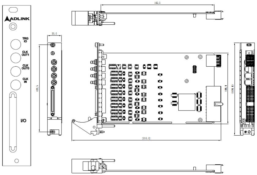
![ADLINK\nTRG IO\nCLK OUT1\nCLK OUT0\nCLK IN\nI/O\n122.5\n30.0\n182.0\n(210.0)](.pxi-2020-2022-50-17032-2010-004-final/181f085a652f4f5886f1b95c1d44c9f8e42cee3ddac2a53cd8a2c352e33a2e1c.jpg)

Figure 2-1: PXI-2020/2022 PCB Layout

The ADLINK PXI-2020/2022 is packaged in a Euro-card form factor compliant with PXI specifications measuring 160 mm in length and 100 mm in height (not including connectors). The connector types and functions are described as follows.

# SMB Connector

 SMB Connector 1: TRG IO
 SMB Connector 2: Sync CLK\_OUT1
 SMB Connector 3: Sync CLK\_OUT0
 SMB Connector 4: CLK IN

<table><tr><td>Connector</td><td>Direction</td><td>Type</td><td>Description/Function</td></tr><tr><td>TRG IO</td><td>Input Output</td><td>SMB</td><td>The TRG IO is a bidirectional port for external digital trigger input or output.</td></tr><tr><td>CLK OUT1</td><td>Output</td><td>SMB</td><td>The CLK OUTOUT 1 is a 50Ω, DC-coupled output; CLK_OUT0 and CLK_OUT1 is from the same source.</td></tr><tr><td>CLK OUT0</td><td>Output</td><td>SMB</td><td>The CLK OUTPUT 0 is a 50Ω, DC-coupled output; CLK_OUT0 and CLK_OUT1 is from the same source.</td></tr><tr><td>CLK IN</td><td>Input</td><td>SMB</td><td>The CLK IN is a 50Ω, AC-coupled external time-base input.</td></tr></table>

Table 2-1: SMB Connector

<table><tr><td colspan="2">TRG IO, as an Input Port</td></tr><tr><td>Connector type</td><td>SMB</td></tr><tr><td>Compatibility</td><td>3.3 V LVTTL(Low Voltage), 5 V tolerant</td></tr><tr><td>Input Logic Level</td><td>Input Low voltage: 0.8V (max)Input high voltage: 2.0 (min)</td></tr><tr><td>Maximum Input Overload</td><td>-0.5 V to +5.5 V</td></tr><tr><td>Trigger Polarity</td><td>Rising edge or falling edge (Software programmable)</td></tr><tr><td>Minimum Pulse Width</td><td>12.5 ns</td></tr></table>

Table 2-2: TRG IO, as an Input Port

<table><tr><td colspan="2">TRG IO, as an Output Port</td></tr><tr><td>Connector type</td><td>SMB</td></tr><tr><td>Compatibility</td><td>3.3 V TTL</td></tr><tr><td rowspan="2">Output Logic Level</td><td>Output low voltage: 0.2 V (max)</td></tr><tr><td>Output high voltage: 2.4 V (min)</td></tr><tr><td>Driving Capability</td><td>8 mA</td></tr><tr><td>Minimum Output Pulse Width</td><td>12.5 ns</td></tr></table>

Table 2-3: TRG IO, as an Output Port

<table><tr><td colspan="2">CLK IN (External Clock from Front Panel)</td></tr><tr><td>Connector Type</td><td>SMB</td></tr><tr><td>Clock Type</td><td>Sine wave or square wave</td></tr><tr><td>Input Impedance</td><td>50 Ω</td></tr><tr><td>Input Coupling</td><td>AC</td></tr><tr><td>Input Range</td><td>1 VP-P to 2 VP-P</td></tr><tr><td>Overvoltage Protection</td><td>2.5 VP-P</td></tr></table>

Table 2-4: CLK IN

<table><tr><td colspan="2">CLK OUT0/OUT1, as an Output Port</td></tr><tr><td>Connector Type</td><td>SMB</td></tr><tr><td>Clock Type</td><td>square wave</td></tr><tr><td>Compatibility</td><td>3.3 V TTL</td></tr><tr><td rowspan="2">Output Logic Level</td><td>Output low voltage: 0.2 V (max)</td></tr><tr><td>Output high voltage: 2.4 V (min)</td></tr><tr><td>Driving Capability</td><td>24 mA</td></tr><tr><td>Output Impedance (for minimum load)</td><td>50 Ω</td></tr></table>

Table 2-5: CLK OUT0/OUT1, as an Output Port

# 2.4 Installing the module

To install the PXI-2020/2022 module:

1. Turn off the PXI system/chassis and disconnect the power plug from the power source.
2. Align the module’s edge with the card guide in the PXI chassis.
3. Slide the module into the chassis, until resistance is felt from the PXI connector.
4. Push the ejector upwards and fully insert the module into the chassis.
5. Once inserted, a “click” can be heard from the ejector latch.
6. Tighten the screw on the front panel.
7. Power on the PXI system/chassis.

To remove the module, reverse step 2 through 6 above.

# 2.5 Software Support

ADLINK provides comprehensive software drivers and packages to suit various user approaches to building a system. Aside from programming libraries, such as DLLs, for most Windows-based systems, ADLINK also provides drivers for other application environment such as LabVIEW® and MATLAB®. ADLINK also provides ActiveX component ware for measurement and SCADA/ HMI, and breakthrough proprietary software applications. All software options are included in the ADLINK All-in-One DVD.

# Programming Library

For customers who are writing their own programs, we provide function libraries for many different operating systems, including:

# D2K-DASK:

Include device drivers and DLL for Windows 98/NT/2000/XP/Vista/ 7. DLL is binary compatible across Windows 98/NT/2000/XP/ Vista/7. This means all applications developed with D2K-DASK are compatible across Windows 98/NT/2000/XP/Vista/7. The developing environment can be VB, VC++, Delphi, BCB6, or any Windows programming language that allows calls to a DLL. The user’s guide and function reference manual of D2K-DASK are in the CD.

# 2.6 PCI Configuration

# 1. Plug and Play:

As a plug and play component, the card requests an interrupt number via its PCI controller. The system BIOS responds with an interrupt assignment based on the card information and on known system parameters. These system parameters are determined by the installed drivers and the hardware load seen by the system.

# 2. Configuration:

The board configuration is done on a board-by-board basis for all PCI boards on your system. Because configuration is controlled by the system and software, there is no jumper setting required for base-address, DMA, and interrupt IRQ.

The configuration is subject to change with every boot of the system as new boards are added or removed.

# 3. Trouble shooting:

If your system doesn’t boot or if you experience erratic operation with your PCI board in place, it’s likely caused by an interrupt conflict (perhaps the BIOS Setup is incorrectly configured). In general, the solution, once you determine it is not a simple oversight, is to consult the BIOS documentation that comes with your system.

# 3 Signal Connections

This chapter describes the connectors of the PXI-2020/2022, and the signal connection between the PXI-2020/2022 and external devices.

# 3.1 Connectors Pin Assignment

The PXI-2020/2022 is equipped with one 68-pin VHDCI-type connector (ACL-10568-1). It is used for digital input/output, analog input, and ti-mer/counter signals, etc. The pin assignments of the connectors are de-fined in Table 3-1 and Figure 3-2.

Connector Pin Assignment

<table><tr><td></td><td>Pin #</td><td>Pin #</td><td></td></tr><tr><td>DGND</td><td>34</td><td>68</td><td>DGND</td></tr><tr><td>DIO1</td><td>33</td><td>67</td><td>DIO0</td></tr><tr><td>DIO3</td><td>32</td><td>66</td><td>DIO2</td></tr><tr><td>DGND</td><td>31</td><td>65</td><td>AFI0/AD TRIG Out</td></tr><tr><td>AFI1/AD TIMER OUT</td><td>30</td><td>64</td><td>AFI2/GPTC_CLK0</td></tr><tr><td>DGND</td><td>29</td><td>63</td><td>AFI3/GPTC_GATE0</td></tr><tr><td>AFI4/GPTC_CLK1</td><td>28</td><td>62</td><td>AFI5/GPTC_GATE1</td></tr><tr><td>AFI6/GPTC_Out1</td><td>27</td><td>61</td><td>AFI7/GPTC_Out0</td></tr><tr><td>NC</td><td>26</td><td>60</td><td>NC</td></tr><tr><td>NC</td><td>25</td><td>59</td><td>NC</td></tr><tr><td>AIL0</td><td>24</td><td>58</td><td>AIH0</td></tr><tr><td>AIL8</td><td>23</td><td>57</td><td>AIH8</td></tr><tr><td>AGND</td><td>22</td><td>56</td><td>AGND</td></tr><tr><td>AIL1</td><td>21</td><td>55</td><td>AIH1</td></tr><tr><td>AIL9</td><td>20</td><td>54</td><td>AIH9</td></tr><tr><td>AGND</td><td>19</td><td>53</td><td>AGND</td></tr><tr><td>AIL2</td><td>18</td><td>52</td><td>AIH2</td></tr><tr><td>AIL10</td><td>17</td><td>51</td><td>AIH10</td></tr><tr><td>AGND</td><td>16</td><td>50</td><td>AGND</td></tr><tr><td>AIL3</td><td>15</td><td>49</td><td>AIH3</td></tr></table>

Table 3-1: PXI-2020/2022 68-pin VHDCI-type Pin Assignment

<table><tr><td>AIL11</td><td>14</td><td>48</td><td>AIH11</td></tr><tr><td>AGND</td><td>13</td><td>47</td><td>AGND</td></tr><tr><td>AIL4</td><td>12</td><td>46</td><td>AIH4</td></tr><tr><td>AIL12</td><td>11</td><td>45</td><td>AIH12</td></tr><tr><td>AGND</td><td>10</td><td>44</td><td>AGND</td></tr><tr><td>AIL5</td><td>9</td><td>43</td><td>AIH5</td></tr><tr><td>AIL13</td><td>8</td><td>42</td><td>AIH13</td></tr><tr><td>AGND</td><td>7</td><td>41</td><td>AGND</td></tr><tr><td>AIL6</td><td>6</td><td>40</td><td>AIH6</td></tr><tr><td>AIL14</td><td>5</td><td>39</td><td>AIH14</td></tr><tr><td>AGND</td><td>4</td><td>38</td><td>AGND</td></tr><tr><td>AIL7</td><td>3</td><td>37</td><td>AIH7</td></tr><tr><td>AIL15</td><td>2</td><td>36</td><td>AIH15</td></tr><tr><td>AGND</td><td>1</td><td>35</td><td>AGND</td></tr></table>

Table 3-1: PXI-2020/2022 68-pin VHDCI-type Pin Assignment Legend:

<table><tr><td>Pin #</td><td>Signal Name</td><td>Reference</td><td>Direction</td><td>Description</td></tr><tr><td>58, 55, 52, 49, 46, 43, 40,37, 57, 54, 51, 48, 45, 42, 39, 36</td><td>AIH &lt;0..15&gt;</td><td>AIL &lt;0..15&gt;</td><td>Input</td><td>Differential positive input for AI channel &lt;0..15&gt;</td></tr><tr><td>29, 31, 34, 68,</td><td>DGND</td><td>----</td><td>----</td><td>Digital ground</td></tr><tr><td>24, 21, 18, 15, 13, 9, 6, 3, 23, 20, 17, 14, 11, 8, 5, 2</td><td>AIL &lt;0..15&gt;</td><td>----</td><td>Input</td><td>Differential negative input for AIL channels &lt;0..15&gt;</td></tr><tr><td>1, 4, 7, 10, 13, 16, 19, 22, 35, 38, 41, 44, 47, 50, 53, 56</td><td>AGND</td><td>----</td><td>----</td><td>Analog ground for AI</td></tr><tr><td>65</td><td>AFI0</td><td>DGND</td><td>In-put/Output</td><td>Auxiliary Function Input 0 (AD_TRIG_SRC0, AD TIMER_SRC0, AD_CONV_SRC0)/AD TRIG Out</td></tr><tr><td>30</td><td>AFI1</td><td>DGND</td><td>In-put/Output</td><td>Auxiliary Function Input 1 (AD_TRIG_SRC1, AD_TIMER_SRC1, AD_CONV_SRC1)/(AD SAMPLE CLK Out)</td></tr></table>

Table 3-2: 68-pin VHDCI-type Connector Legend

<table><tr><td>Pin #</td><td>Signal Name</td><td>Reference</td><td>Direction</td><td>Description</td></tr><tr><td>64</td><td>AFI2</td><td>DGND</td><td>Input</td><td>Auxiliary Function Input 2 (AD_TRIG_SRC2,AD_TIMER_SRC2,AD_CONV_SRC2)/(GPTC_CLK0)</td></tr><tr><td>63</td><td>AFI3</td><td>DGND</td><td>Input</td><td>Auxiliary Function Input 3 (AD_TRIG_SRC3,AD_TIMER_SRC3,AD_CONV_SRC3)/(GPTC_GATE0)</td></tr><tr><td>28</td><td>AFI4</td><td>DGND</td><td>Input</td><td>Auxiliary Function Input 4 (AD_TRIG_SRC4,AD_TIMER_SRC4,AD_CLK_SRC4)/(GPTC_CLK1)</td></tr><tr><td>62</td><td>AFI5</td><td>DGND</td><td>Input</td><td>Auxiliary Function Input 5 (AD_TRIG_SRC5,AD_TIMER_SRC5,AD_CONV_SRC5)/(GPTC_GATE1)</td></tr><tr><td>27</td><td>AFI6</td><td>DGND</td><td>In-put/Output</td><td>Auxiliary Function Input 6 (AD_TRIG_SRC6,AD_TIMER_SRC6,AD_CLK_SRC6)/(GPTC_OUT1)</td></tr><tr><td>61</td><td>AFI7</td><td>DGND</td><td>In-put/Output</td><td>Auxiliary Function Input 7 (AD_TRIG_SRC7,AD_TIMER_SRC7,AD_CLK_SRC7)/(GPTC_OUT0)</td></tr><tr><td>67, 33, 66, 32</td><td>DIO&lt;0..3&gt;</td><td>DGND</td><td>In-put/Output</td><td>Programmable DIO pins</td></tr><tr><td>25, 26, 59, 60</td><td>NC</td><td>DGND</td><td>----</td><td>----</td></tr></table>

Table 3-2: 68-pin VHDCI-type Connector Legend
Note: Pins 2, 5, 8, 11, 14, 17, 20, 23, 36, 39, 42, 45, 48, 51, 54, and 57 are NC for the PXI-2020.

# 3.2 Analog Input Signal Connection

The PXI-2020/2022 provides 8/16 differential analog input channels. The analog signal can be converted to digital values by the A/D converter. To avoid ground loops and obtain more accurate measurements from the A/D conversion, it is quite important to understand the signal source type and how to connect the analog input signals.

# 3.2.1 Types of Signal Sources

# Ground-Referenced Signal Sources

A ground-referenced signal means it is connected in some way to the building system. That is, the signal source is already connected to a common ground point with respect to the PXI-2020/ 2022, assuming that the computer is plugged into the same power system. Non- isolated outputs of instruments and devices that plug into the buildings power system are ground-referenced signal sources.

# Floating Signal Sources

A floating signal source means it is not connected in any way to the buildings ground system. A device with an isolated output is a floating signal source, such as optical isolator outputs, transformer outputs, and thermocouples.

# 3.2.2 Input Connect Configurations - Differential Input Mode
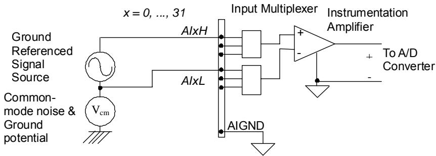
![This flowchart depicts a signal acquisition circuit with the following components and connections:\n\n**Left Side (Signal Source):**\n*   **Text:** 'Ground Referenced Signal Source' is positioned to the left of an AC voltage source symbol (a circle with a sine wave).\n*   **Text:** 'Common-mode noise & Ground potential' is positioned below the signal source.\n*   **Component:** A DC voltage source labeled '\$V_{\text{cm}}\$' is connected in series with the AC source. Its bottom terminal connects to a ground symbol.\n*   **Connections:**\n    *   The top terminal of the AC source connects to a wire labeled '**AlxH**'. Above this wire is the text '**x = 0, ..., 31**'.\n    *   The wire connecting the AC source and the \$V_{\text{cm}}\$ source is labeled '**AlxL**'.\n\n**Middle Section (Bus and Multiplexer):**\n*   **Vertical Bus:** A vertical line with multiple connection dots connects the signal lines.\n    *   The top dot connects to '**AlxH**'.\n    *   The middle section contains connection dots feeding into the multiplexer blocks.\n    *   A dot connects to '**AlxL**'.\n    *   The bottom dot connects to '**AIGND**', which leads to a ground symbol.\n*   **Text:** '**Input Multiplexer**' is centered above two rectangular blocks.\n*   **Connections:**\n    *   Three lines from the vertical bus connect to the left side of the top rectangular block.\n    *   Three lines from the vertical bus connect to the left side of the bottom rectangular block.\n\n**Right Side (Amplifier and Output):**\n*   **Text:** '**Instrumentation Amplifier**' is above a triangle symbol representing an op-amp.\n*   **Connections:**\n    *   The output of the top multiplexer block connects to the non-inverting input (**'+'**) of the amplifier.\n    *   The output of the bottom multiplexer block connects to the inverting input (**'-'**) of the amplifier.\n    *   The inverting input (**-**) is also connected to a ground symbol.\n*   **Output:** The output line extends to the right.\n    *   Text above the line reads '**To A/D Converter**'.\n    *   Labels **'+'** and **'- '** are present near the output terminals.](.pxi-2020-2022-50-17032-2010-004-final/7c4085cde3069ab36bc386f12da637ea83cfa1f8194ddcad37597e57609604df.jpg)

Figure 3-1: Ground-referenced Source and Differential Input

The differential input mode provides two inputs that respond to signal voltage difference between them. If the signal source is ground-referenced, the differential mode can be used for the common-mode noise rejection. Figure 3-1 shows the connection of ground-referenced signal sources under differential input mode.

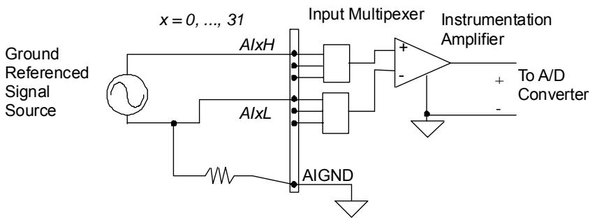
Figure 3-2 shows how to connect a floating signal source to the PXI-2020/2022 card in differential input mode. For floating signal sources, you need to add a resistor at each channel to provide a bias return path. The resistor value should be about 100 times the equivalent source impedance. If the source impedance is less than 100ohms, you can simply connect the negative side of the signal to AIGND as well as the negative input of the Instru-mentation Amplifier without any resistors. In differential input mode, less noise couples into the signal connections than in single-ended mode.
![Based on the provided flowchart/block diagram, here is an accurate and concise description:\n\n**Labeled Blocks and Components:**\n*   **Ground Referenced Signal Source:** Represented by a circle with a sine wave inside.\n*   **Input Multiplexer:** Represented by two rectangular blocks.\n*   **Instrumentation Amplifier:** Represented by a triangle.\n*   **Resistor:** Located on the bottom wire from the signal source.\n*   **Vertical Bus Bar:** A vertical line with dots connecting the signal source to the multiplexer.\n\n**Text Labels:**\n*   'Ground Referenced Signal Source'\n*   'x = 0, ..., 31' (above the vertical bus bar)\n*   'A1xH'\n*   'A1xL'\n*   'A1GND'\n*   'Input Multiplexer'\n*   'Instrumentation Amplifier'\n*   '+'\n*   '-'\n*   'To A/D Converter'\n\n**Connections:**\n*   **Signal Source to Bus Bar:**\n    *   The top wire from the 'Ground Referenced Signal Source' connects to the vertical bus bar and is labeled 'A1xH'.\n    *   The middle wire from the source connects to the vertical bus bar and is labeled 'A1xL'.\n    *   The bottom wire from the source passes through a resistor and connects to the bus bar at a point labeled 'A1GND'.\n*   **Bus Bar to Input Multiplexer:**\n    *   The vertical bus bar (labeled 'x = 0, ..., 31') connects to both blocks of the 'Input Multiplexer'.\n*   **Input Multiplexer to Instrumentation Amplifier:**\n    *   The top block of the 'Input Multiplexer' connects to the '+' input of the 'Instrumentation Amplifier'.\n    *   The bottom block of the 'Input Multiplexer' connects to the '-' input of the 'Instrumentation Amplifier'.\n*   **Instrumentation Amplifier Ground:**\n    *   The bottom vertex of the amplifier triangle is connected to a ground symbol.\n*   **Amplifier Output:**\n    *   The output (right side) of the 'Instrumentation Amplifier' connects to a line labeled 'To A/D Converter'.\n    *   Near the end of this line, there are '+' and '-' signs. The '-' sign is connected to a ground symbol.](.pxi-2020-2022-50-17032-2010-004-final/cc73bb37c10c57b671d54a9270d480abf51d5761ab9f2f1bd6f1b33cc8798fa0.jpg)

Figure 3-2: Floating Source and Differential Input

# 4 Function Block and Operation Theory

The operation theory of the functions on the PXI-2020/2022 is described in this chapter. The functions include the A/D conversion, Digital I/O and General Purpose Counter/Timer. The operation theory can help you understand how to configure and program the PXI-2020/2022.

The entire PXI-2020 series of cards includs the PXI-2020/2022. In the PXI-2022 cards, all the A/D related timings are for simultaneously A/D sampling based on scanning, so that PXI-2022 also adopts the same concept, except there is only one conversion signal in a scan which could generate up to 16 samples from the different 16 channels at the same time. In the following description, to conform to the original timing design, we still use “scan” as the unit of A/D data acquisition.

# 4.1 Overall Function Block Diagram
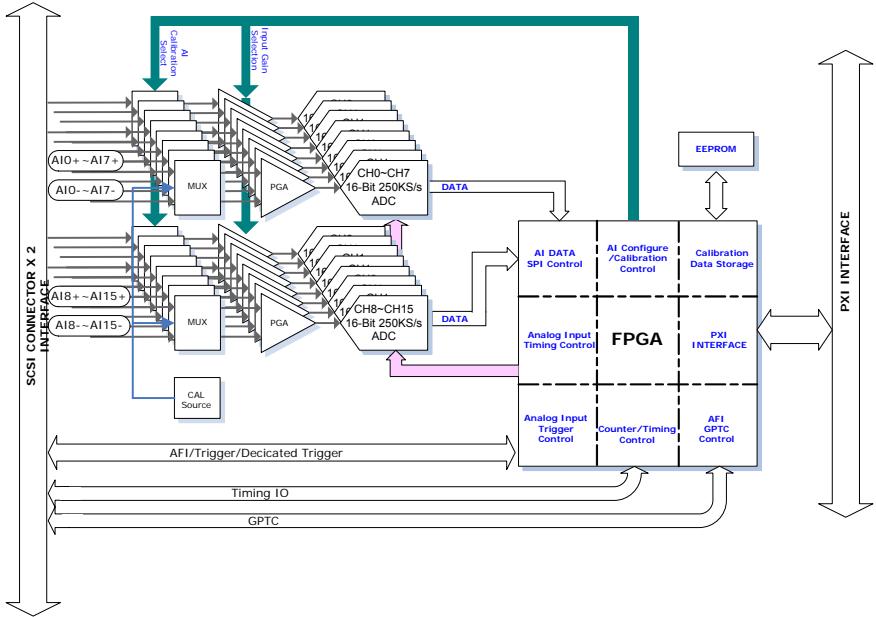
![Based on the provided flowchart, here is the accurate and concise description of the labeled blocks and their connections:\n\n**Labeled Blocks**\n\n*   **Interfaces:**\n    *   'SCSI CONNECTOR X 2 INTERFACE' (vertical label on the left)\n    *   'PXI INTERFACE' (vertical label on the right)\n    *   'PXI INTERFACE' (sub-block within the FPGA)\n*   **Input Channels & Sources:**\n    *   'A10~ + -A17 +'\n    *   'A10~ - -A17 -'\n    *   'A18~ + -A15 +'\n    *   'A18~ - -A15 -'\n    *   'CAL Source'\n    *   'AFI/Trigger/Decicated Trigger'\n    *   'Timing IO'\n    *   'GPTC'\n*   **Signal Conditioning & Conversion:**\n    *   Two blocks labeled 'MUX'\n    *   Two blocks labeled 'PGA'\n    *   'CH0-CH7 16-Bit 250KS/s ADC'\n    *   'CH8-CH15 16-Bit 250KS/s ADC'\n*   **Control Inputs:**\n    *   'AFI'\n    *   'Calibration'\n    *   'Selection'\n    *   'Input Gain'\n*   **FPGA Sub-blocks:**\n    *   'AI DATA SPI Control'\n    *   'AI Configure /Calibration Control'\n    *   'Calibration Data Storage'\n    *   'Analog Input Timing Control'\n    *   'Analog Input Trigger Control'\n    *   'Counter/Timing Control'\n    *   'AFI GPTC Control'\n*   **Memory:**\n    *   'EEPROM'\n\n**Connections**\n\n*   **Input Paths:**\n    *   'A10~ + -A17 +' and 'A10~ - -A17 -' connect to the top 'MUX'.\n    *   'A18~ + -A15 +' and 'A18~ - -A15 -' connect to the bottom 'MUX'.\n    *   A blue line connects 'A10~ + -A17 +' to the bottom 'MUX'.\n    *   'CAL Source' connects to the bottom 'MUX'.\n*   **Control & Feedback:**\n    *   'AFI' connects to the top 'MUX'.\n    *   'Calibration', 'Selection', and 'Input Gain' connect to the top 'PGA'.\n    *   A large teal arrow loops from the FPGA area back to the 'Input Gain' control section.\n*   **Data Flow to FPGA:**\n    *   'DATA' flows from 'CH0-CH7 16-Bit 250KS/s ADC' to 'AI DATA SPI Control'.\n    *   'DATA' flows from 'CH8-CH15 16-Bit 250KS/s ADC' to 'AI DATA SPI Control'.\n*   **Trigger/Clock Signals:**\n    *   Pink arrows connect 'Analog Input Trigger Control' to 'CH0-CH7 16-Bit 250KS/s ADC' and 'Counter/Timing Control' to 'CH8-CH15 16-Bit 250KS/s ADC'.\n*   **External Controls:**\n    *   'AFI/Trigger/Decicated Trigger' connects to 'Analog Input Trigger Control'.\n    *   'Timing IO' connects to 'Counter/Timing Control'.\n    *   'GPTC' connects to 'AFI GPTC Control'.\n*   **Inter-block Connections:**\n    *   A double-headed arrow connects 'EEPROM' and 'Calibration Data Storage'.\n    *   A double-headed arrow connects the 'PXI INTERFACE' sub-block and the right vertical 'PXI INTERFACE' label.](.pxi-2020-2022-50-17032-2010-004-final/aee677ec053cb70693cd9f02c5a73240b143ae6a00577d0e7b925b045c4698f3.jpg)

Figure 4-1: PXI-2022 Functional Block Diagram

# 4.2 Basic AI Acquisition

In this section, the basic acquisition timing is explained.

# 4.2.1 Analog Input Path

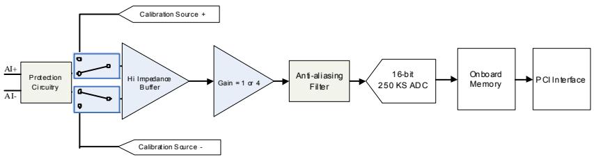
The following figure shows the block diagram of the single analog input path of a PXI-2020/2022. Each path provides a choice of 1G Ω input impedance or high impedance. The gain amplifier is optimized for ±10 V and ±2.5 V input range with low noise and high dynamic range. An anti-aliasing filter is also adopted to eliminate high frequency noise. The 16-bit ADC provides not only accurate DC performance but also high signal-to-noise ratio, high spuriousfree dynamic range in AC performance.
![**Labeled Blocks:**\n*   AI+\n*   AI-\n*   Protection Circuitry\n*   Calibration Source +\n*   Calibration Source -\n*   Hi Impedance Buffer\n*   Gain = 1 or 4\n*   Anti-aliasing Filter\n*   16-bit 250 KS ADC\n*   Onboard Memory\n*   PCI Interface\n\n**Connections:**\n*   **AI+** and **AI-** feed into the **Protection Circuitry**.\n*   The **Protection Circuitry** connects to a block containing two switches.\n*   **Calibration Source +** connects to the upper input of the switch block.\n*   **Calibration Source -** connects to the lower input of the switch block.\n*   The switch block connects to the **Hi Impedance Buffer**.\n*   The **Hi Impedance Buffer** connects to the **Gain = 1 or 4** block.\n*   The **Gain = 1 or 4** block connects to the **Anti-aliasing Filter**.\n*   The **Anti-aliasing Filter** connects to the **16-bit 250 KS ADC**.\n*   The **16-bit 250 KS ADC** connects to the **Onboard Memory**.\n*   The **Onboard Memory** connects to the **PCI Interface**.](.pxi-2020-2022-50-17032-2010-004-final/3008d13ff2185567e9a62aa9429cb19e600332afdc50ccf051c7906d3c56d189.jpg)

Figure 4-2: PXI-2020/2022 Analog Input Path

# 4.2.2 Basic Acquisition Timing

The trigger is a signal that starts or stops the acquisition. In posttrigger mode and delay trigger mode, the trigger is used to initiate acquisition. In pre-trigger mode, the trigger is used to stop acquisition. In middle-trigger mode, the trigger is used to inform the acquisition engine to acquire the specific number of data and then stop.

Timebase is a clock that sent to the ADC of each channel and the acquisition engine for essential timing functionality. The source of timebase can be either internal oscillator or external clock generator. Usually the maximum sampling rate of a Data Acquisition Module is determined by the speed of timebase. However, other sampling rate can be achieved by specifying a scan interval counter. Please refer to Table 4-1 below and Section “4.3.4” on page 30 for more details.

<table><tr><td>Counter Name</td><td>Length</td><td>Valid value</td><td>Description</td></tr><tr><td>ScanIntrv</td><td>32-bit</td><td>4 to 4294967296</td><td>Scan Interval Counter.This counter is a TIMEBASE(80MHz) divider to the achieve equivalent sam-pling rate of DAQ. The equation is:Sampling rate = TIMEBASE / ScanIntrvThe value of TIMEBASE de-pends on the card type. Take PXI-2022 (250KS/s) as an example, the ScanIntrv = 320 results in 250KS/s and Sca-nIntrv = 640 results in 125KS/s, and so on.</td></tr><tr><td>DataCnt</td><td>31-bit</td><td>1 to 2147483648</td><td>Data Counter.The amount of data to be acquired can be specified. The PXI-2022 includes 8 K sample space to store acquired data.</td></tr><tr><td>trigDelayTicks</td><td>32-bit</td><td>1 to 536870911</td><td>Delay Trigger Counter.The delay trigger counter is used to indicate the time be-tween a trigger event and the start of an acquisition. The unit of a delay count is the period of the TIMEBASE. For PXI-2022, the unit is 100ns. Refer to sec-tion 3.5.4 for more detail.</td></tr><tr><td>ReTrgCnt</td><td>32-bit</td><td>1 to 4294967296</td><td>Re-Trigger Counter.The DAQ can enable re-trigger to accept multiple triggers. Refer to section 4.5.5 for more details.</td></tr></table>

Table 4-1: Basic Counters

Refer to Figure 4-3 and use the post trigger mode as an example. When a trigger is accepted by data acquisition module, the acquisition engine of the card will begin to acquire data that coming from ADC and store these sampled data to onboard memory. The sampled data is generated con-tinuously at the rising edge of timebase according to the scan interval counter setting. While sampled data reaches customer specified number, in the below example is 256, the acquisition ends. Once the acquisition ends, acquisition engine begins to send request to system and transfer data from onboard memory back to system by DMA.

![Based on the provided image, here is the accurate and concise description of the flowchart/block diagram:\n\n**Labeled Blocks and Content:**\n\n*   **Analog signal**: A sine wave waveform with small black dots marking specific points on the curve.\n*   **TIMEBASE**: A square wave clock signal with upward-pointing arrows on the rising edges. The black dots from the 'Analog signal' align vertically with these rising edges.\n*   **Trigger**: A pulse waveform that goes high and remains high for three clock cycles before dropping low.\n*   **Acquisition In Progress**: A signal line that transitions from low to high. A text annotation reads 'Acquisition starts right after this clock edge' with an arrow pointing to the rising edge of the TIMEBASE wave immediately following the drop of the Trigger pulse.\n*   **DATA**: A sequence of rectangular boxes connected by a horizontal line. The sequence is labeled 'D1', 'D2', 'D3', 'D4', followed by ellipses, then 'D253', 'D254', 'D255', 'D256'.\n*   **Footer Text**: 'Trigger mode = post-trigger, DataCnt = 256, ScanIntrv = 1'\n\n**Connections and Relationships:**\n\n*   **Sampling**: The black dots on the **Analog signal** indicate that the signal is being sampled at the rising edges of the **TIMEBASE**.\n*   **Timing Sequence**: The **Trigger** pulse occurs first. Once it drops low, the **Acquisition In Progress** signal goes high (starting immediately after a specific clock edge).\n*   **Data Acquisition**: The sequence of **DATA** boxes (from D1 to D256) corresponds temporally to the duration where **Acquisition In Progress** is high.](.pxi-2020-2022-50-17032-2010-004-final/7e17063e062efce2b083b599f5fa17fa07fc354fd1d90e9e1a6310e7d020da5c.jpg)

Figure 4-3: Basic Acquisition Timing of PXI-2020/2022

# 4.2.3 AI Data Format

When using an A/D converter, users should first know about the properties of the signal to be measured. Users can decide which channel to use and how to connect the signals to the card. Please refer to 4.2 for signal con-nections.

The A/D acquisition is initiated by a trigger source; users must decide how to trigger the A/D conversion. The data acquisition will start once a trigger condition is matched. After the end of an A/D conversion, the A/D data is buffered in a Data FIFO. The A/D data can now be transferred into the PC's memory for further processing.

Two acquisition modes, Software Polling and Scan acquisition are de-scribed below. Timing, trigger modes, trigger sources, and transfer me-thods are included in this section. The following table illustrates the idea transfer characteristics of various input ranges of the PXI-2020/2022. The data format of the PXI-2020/2022 is straight binary.

<table><tr><td>Description</td><td colspan="2">Bipolar Analog Input Range</td><td>Digital code</td></tr><tr><td>Full-scale Range</td><td>±10 V</td><td>±2.5 V</td><td></td></tr><tr><td>Least significant bit</td><td>305.2 uV</td><td>76.3 uV</td><td></td></tr><tr><td>FSR-1LSB</td><td>9.999695 V</td><td>2.499924 V</td><td>7FFF</td></tr><tr><td>Midscale +1LSB</td><td>305.2uV</td><td>76.3 uV</td><td>0001</td></tr><tr><td>Midscale</td><td>0 V</td><td>0 V</td><td>0000</td></tr><tr><td>Midscale -1LSB</td><td>-305.2 uV</td><td>-76.3 uV</td><td>FFFF</td></tr><tr><td>-FSR</td><td>-10 V</td><td>-2.5 V</td><td>8000</td></tr></table>

Table 4-2: Bipolar Analog Input Range and Output Digital Code

# 4.3 ADC Sampling Rate and TIMEBASE Control

The PXI-2022 supports six timebase sources for analog input conversion:

1. On board Internal oscillator
2. External clock through front panel (AFI[0..7])
3. External clock through front panel SMB CLK IN
4. PXI Star Trigger
5. PXI Trigger Bus Line 0
6. PXI 10M

The following diagram shows the timebase architecture of the PXI-2022.

![Based on the provided flowchart, here are the labeled blocks and their connections:\n\n**Input Sources and Clock Generation:**\n*   **Ext. CLK IN** connects to an **SMB Connector** (depicted as a circle with a ground symbol).\n*   The **SMB Connector** connects to a **CLK Buffer** (triangle).\n*   The **CLK Buffer** output connects to the **Timebase Clock Mux**.\n*   An **Onboard Oscillator** (rounded rectangle) connects directly to the **Timebase Clock Mux**.\n\n**Digital Inputs to Multiplexer:**\n*   Four horizontal lines with labels connect directly to the **Timebase Clock Mux**:\n    *   **AFI(0..7)**\n    *   **PXI_STAR**\n    *   **PXI_10M**\n    *   **PXI Trigger Bus Line 0**\n*   On the far left, a vertical double-headed arrow labeled **SCSI** is shown above another vertical double-headed arrow labeled **PXI Interface**, which groups the four digital input lines listed above.\n\n**Multiplexer and Clock Distribution:**\n*   The **Timebase Clock Mux** (trapezoid) has two outputs:\n    1.  One output connects to a **1-to-16 Clock Buffer** (triangle).\n    2.  Another output extends to the right, labeled **PXI Trigger Bus Line 0**.\n*   The **1-to-16 Clock Buffer** splits into multiple outputs on the right side:\n    *   **ADC0**\n    *   **ADC1**\n    *   (indicated by dots)\n    *   **ADC15**\n\n**Outputs:**\n*   The right-side **PXI Trigger Bus Line 0** connects to a vertical double-headed arrow labeled **PXI Interface**.](.pxi-2020-2022-50-17032-2010-004-final/6a6375cde9657d59767feec7dfa2dd00ac548a17eaf9162d8c1071f62e49756c.jpg)

Figure 4-4: PXI-2022 Timebase Source and Architecture.

# 4.3.1 Internal Oscillator

The PXI-2020/2022 equips a high stability, low jitter oscillator for the ADCs. The oscillators are 80 MHz for the PXI-2020/2022.

# 4.3.2 External Clock through Front Panel

When you need a specific timebase in some applications that the onboard oscillator is not achievable, a clock from an external device can replace onboard oscillator. In addition, external timebase also provides a method to synchronize the DAQ module to other measurement modules by distribut-ing/receiving a common clock to/from multiple modules. The PXI-2020/2022 can receive an external timebase from the front panel connector AFI[0…7] or the SMB CLK IN.

As you supply the timebase from external SMB CLK IN, which should be a sine wave or square wave signal. This signal is AC coupled with 50Ω input impedance and the valid input level is from 1 to 2 volts peak-to-peak. Note that the external clock should be continuous for fix sampling rate ADC operation.

# 4.3.3 External Clock from PXI Interfaces

The PXI-2020/2022 can receive timebase via the PXI Trigger Bus line 0 by software setting. The eight PXI Trigger Bus lines (PXI\_TRIG[0..7]) provide inter-module synchronization and communication. Note that this function is only available when the PXI-2020/2022 is in a PXI system. It’s not supported when PXI-2020/ 2022 is in a CompactPCI system. When the PXI-2020/2022 is plugged into a generic peri-pheral slot in a PXI system, it can receive timebase from PXI\_STAR. The PXI\_STAR signal comes from star trigger controller is matched in propagation delay within 1 ns and the delay from star trigger slot to peripheral slot is less than 5 ns. According these hardware features, the PXI-2020/2022 can achieve very good synchronization performance when using PXI\_STAR as timebase clock source. Note that the function is only available when the PXI-2020/2022 is in a PXI system. It’s not supported when the PXI-2020/2022 is in a CompactPCI system.

# 4.3.4 Sampling Rate Control

By specifying different scan interval counter (32-bit) value, different sam-pling rate can be achieved. The following formula determines the ADC sampling rate. Sampling Rate = TIMEBASE/Scan-Intrv Where ScanIntrv is scan interval counter, value can be 4, 5, 6, 7, .... 232-1.

![This image is a timing diagram illustrating signal relationships and data acquisition intervals.\n\n**Labeled Blocks and Signals:**\n*   **Top Signal:** A square wave labeled **'Trigger'**.\n*   **Second Signal:** A square wave labeled **'TIMEBASE'**, featuring upward-pointing arrows on each rising edge.\n*   **Third Section:** A group labeled **'DATA'** with a curly brace encompassing three rows:\n    *   **Row 1:** Labeled **'ScanIntrv = 1'**. It features a continuous sequence of hexagonal blocks connected by a line, labeled sequentially: **'D1'**, **'D2'**, **'D3'**, **'D4'**, **'D5'**, **'D6'**, **'D7'**, **'D8'**, **'D9'**, **'D10'**.\n    *   **Row 2:** Labeled **'ScanIntrv = 2'**. It features hexagonal blocks labeled **'D1'**, **'D2'**, **'D3'**, **'D4'**, **'D5'**, **'D6'** separated by horizontal gaps.\n    *   **Row 3:** Labeled **'ScanIntrv = 3'**. It features hexagonal blocks labeled **'D1'**, **'D2'**, **'D3'**, **'D4'** separated by larger horizontal gaps.\n*   **Bottom Signal:** A line labeled **'Acquisition In Progress'** that transitions from low to high.\n\n**Connections and Annotations:**\n*   The blocks in each 'DATA' row are connected horizontally by a thin line.\n*   There is blue text at the bottom reading **'Acquisition starts right after this clock edge'**, with a blue arrow pointing to the rising edge of the **'Acquisition In Progress'** signal.](.pxi-2020-2022-50-17032-2010-004-final/7c830a2c777a037ba1b6b0fd2ea7eb5a5d2f6a31c7e508b99ea54380f446030d.jpg)

Figure 4-5: Configuring Different Sampling Rate of PXI-2022.

# 4.3.5 Timebase Exporting

The PXI-2020/2022 can export timebase to one of the PXI trigger bus line 0. By software programming, you can pick up a trigger line to transmit timebase clock. This feature is very useful when synchronize to multiple measurement modules.

# 4.4 Trigger Sources

In addition to the internal software trigger, the PXI-2020/2022 supports external digital triggers from the front panel connector AFI[0…7], SMB TRIG I/O, PXI\_STAR triggers, PXI Trigger Bus Line 5. You can configure the trigger source by software command. Please refer to Figure 4-6 for trigger architecture.

![The diagram depicts a signal routing flow from left to right involving inputs, two multiplexers, a decision block, and outputs.\n\n**Labeled Blocks:**\n*   **Trigger Source Mux** (Large trapezoid on the left)\n*   **Trigger Decision** (Square in the center)\n*   **Trigger Output Mux** (Small trapezoid on the right)\n*   **TRG I/O SMB Connector** (Circle with a dot and ground symbol, appearing at the far left and far right)\n\n**Connections:**\n*   **Inputs (Left to Trigger Source Mux):**\n    *   An arrow labeled **'Software Trigger'** points right into the top of the Trigger Source Mux.\n    *   An arrow labeled **'Digital Trigger Input'** originates from the left **TRG I/O SMB Connector** and points right into the Trigger Source Mux.\n    *   A thick arrow labeled **'AFI(0:7)'** points right into the Trigger Source Mux. To its left is a vertical double-headed arrow labeled **'SCSI'**.\n    *   Two thin arrows point right into the Trigger Source Mux: one labeled **'PXI_STAR'** and one labeled **'PXI Trigger Bus Line 5'**. To their left is a vertical double-headed arrow labeled **'PXI Interface'**.\n\n*   **From Trigger Source Mux to Trigger Decision:**\n    *   A single arrow points right from the Trigger Source Mux into the Trigger Decision block.\n\n*   **From Trigger Decision:**\n    *   An arrow points up labeled **'To Internal Circuit'**.\n    *   An arrow points right labeled with the text **'SSI_AD_TRIG'** and **'SSI_START'** below it.\n\n*   **From Trigger Decision to Trigger Output Mux:**\n    *   The arrow labeled **'SSI_AD_TRIG'** and **'SSI_START'** points into the Trigger Output Mux.\n\n*   **Outputs (From Trigger Output Mux):**\n    *   An arrow labeled **'Digital Trigger Input'** points right into the right-side **TRG I/O SMB Connector**.\n    *   A thick arrow labeled **'PXI Trigger Bus(5)'** points right. To its right is a vertical double-headed arrow labeled **'PXI Interface'**.](.pxi-2020-2022-50-17032-2010-004-final/0ef493291ddfc2e33cfa7c1eefa0b8d7d8b4b8b90e5422dfd48dec8895645c59.jpg)

Figure 4-6: PXI-2020/2022 Trigger Sources

# 4.4.1 Software Trigger

Software trigger is generated by software command. The trigger asserts right after executing specified function calls to begin the operation. This is the easiest way to acquire a single A/D data. The A/D converter starts one con-version whenever the dedicated software command is executed. Then the software would poll the conversion status and read the A/D data back when it is available. This method is very suitable for applications that need to process A/D data in real time. Under this mode, the timing of the A/D conversion is fully controlled under software. However, it is difficult to control the A/D conversion rate.

# 4.4.2 External Digital Trigger

An external digital trigger occurs when a TTL rising edge or a falling edge is detected at the SMB connector TRG IO on the front panel. As illustrated in Figure 4-7, the trigger polarity can be selected by software. Note that the signal level of the external digital trigger signal should be TTL-compatible, and the minimum pulse width is 12.5 ns.

![Pulse Width ) 12.5 ns](.pxi-2020-2022-50-17032-2010-004-final/752ae4d72a799546d114aefbd0faef93ff2ff16af960c810e80e604918daf9d0.jpg)

Rising edge trigger event

![Pulse Width ) 12.5 ns](.pxi-2020-2022-50-17032-2010-004-final/3a3d0e5dd5f4d17e91a065e6d359d39c968b805e611685473bd5272fd35ee58a.jpg)

Falling edge trigger event
Figure 4-7: External Digital Trigger Polarity and Pulse Width Re-quirement.

# 4.4.3 PXI Star Trigger

When you select PXI Star Trigger as the trigger source, the PXI-2020/2022 can accept a TTL-compatible digital signal as a trigger signal. The trigger occurs when a rising edge or falling edge is detected at PXI Star Trigger. You can use software to configure the trigger polarity. The minimum pulse width requirement of this digital trigger signal is 12.5 ns.

# 4.4.4 PXI Trigger Bus

The PXI-2020/2022 utilizes PXI Trigger Bus[5] as System Synchronization In-terface (SSI). Using the interconnected bus provided by PXI Trigger Bus, you can easily synchronize multiple modules. When configured as input, the PXI-2020/2022 is served as a slave module and can accept three different SSI signals, SSI\_TIMEBASE (PXI Trigger Bus[0]), PXI Trigger Bus[5] and PXI Star Trigger Bus[1]. When confi-gured as output, the PXI-2020/ 2022 is served as a master module and can output SSI\_TIMEBASE, SSI\_AD\_TRIG or SSI\_ADCONV to PXI Trigger Bus. Each signal is dedicated routed from the PXI Trigger Bus[5].

# 4.4.5 Trigger Signal Exporting

The PXI-2020/2022 can export trigger signals to following connectors/bus: SMB TRG IO on front panel, AFI0 on front panel and PXI Trigger Bus Line 5. The TRG IO on the front panel can also be programmed to output the trigger signal when the trigger source is from software trigger, Auxiliary Function Interface, PXI Star Trigger, or PXI Trigger Bus Line 5. The timing characteristic is in Figure 4-8.

![Tw\nTRG IO\n(Output)\nTw = 3 TIMEBASE Clocks](.pxi-2020-2022-50-17032-2010-004-final/0af73d3a3adcb0f63e7177b393e91974ec2bb4685378e8dd938cac13f21ce66e.jpg)

Figure 4-8: TRG IO Output Signal Timing

# 4.5 User-controllable Timing Signals

In order to meet the requirements for user-specific timing and the re-quirements for synchronizing multiple cards, the PXI-2020/2022 series provides flexible user-controllable timing signals to connect to external circuitry or additional cards.

The entire DAQ timing of the PXI-2020/2022 series is composed of a bunch of counters and trigger signals in the FPGA. These timing signals are related to the A/D conversions and Timer/Counter applications. These timing signals can be inputs to or outputs from the I/O connectors, the SSI connector and the PXI bus. Therefore the internal timing signals can be used to control external devices or circuitry’s. However, the SSI/PXI timing signals remain the same for every PXI-2020/2022 card.

We implemented signal multiplexers in the FPGA to individually choose the desired timing signals for the DAQ operations, as shown in the Figure 4-9.

![Based on the provided image, here is the description of the flowchart:\n\n**Labeled Blocks:**\n*   Internal timing signals\n*   SSI timing Signals\n*   AFI timing signals\n*   DAQ timing signals\n*   SSI timing Signals\n*   Trigger_Out timing signals\n\n**Connections:**\n*   The three leftmost blocks ('Internal timing signals', 'SSI timing Signals', and 'AFI timing signals') each connect via three horizontal lines to a vertical trapezoidal shape.\n*   This left trapezoid connects via three horizontal lines to the central block labeled 'DAQ timing signals'.\n*   The 'DAQ timing signals' block connects via three horizontal lines to a second vertical trapezoidal shape.\n*   This right trapezoid splits the connection: three lines connect to the top-right block ('SSI timing Signals') and three lines connect to the bottom-right block ('Trigger_Out timing signals').](.pxi-2020-2022-50-17032-2010-004-final/e1e785b341444eceecade2554b986e63b3ad8a3048c999d781e2d698a2728f27.jpg)

Figure 4-9: DAQ Signal Routing

You can utilize the flexible timing signals through our software drivers, and simply and correctly connect the signals with the PXI-2020/2022 series cards. Here is the summary of the DAQ timing signals and the corresponding functionalities for PXI-2020/2022 series.

To route an internal signal to the AFIn, PXI STAR Trigger, or the PXI Trigger Bus[5] line, or to enable clock sharing through the PXI trigger bus line or the PXI Star trigger line. please refer to D2K-DASK Function Reference, check the D2K-Route\_Siganl Usage for details.

<table><tr><td>Timing Signal Category</td><td>Corresponding Functionality</td></tr><tr><td>SSI/PXI signals</td><td>Multiple cards synchronization</td></tr><tr><td>AFI signals</td><td>Control PXI-2020/2022 by external timing signals</td></tr><tr><td>SMB CLK IN</td><td>Control PXI-2020/2022 by external timing signals</td></tr><tr><td>AI_Trig_Out</td><td>Control external circuitry or boards</td></tr></table>

Table 4-3: Summary of User-controllable Timing Signals and Corresponding Functionalities

# 4.5.1 DAQ timing signals

The user-controllable internal timing-signals contain: (Please refer to Section 4.1.4 for the internal timing signal definition)

1. TIMEBASE, providing TIMEBASE for all DAQ operations, which could be from internal 80MHz oscillator, EXTTIMEBASE from I/O connector or the SSI\_TIMEBASE (PXI Trigger Bus [5]). Note that the frequency range of the EXTTIMEBASE is 1MHz to 80MHz, and the EXTTIMEBASE should be TTL-compatible.
2. AD\_TRIG, the trigger signal for the A/D operation, which could come from external digital trigger, internal software trigger and SSI\_AD\_TRIG (PXI Trigger Bus [0]). Refer to Section 4.5 for detailed description.
3. SCAN\_START, the signal to start a scan, which would bring the following ADCONV signals for AD conversion, and could come from the internal SI\_counter, AFI[0] and SSI\_AD\_START. This signal is synchronous to the TIMEBASE. Note that the AFI[0] should be TTL-compatible and the minimum pulse width should be the pulse width of the TIMEBASE to guarantee correct functionalities.

4. ADCONV, the conversion signal to initiate a single conversion, which could be derived from internal counter, AFI[0] or SSI\_ADCONV. Note that this signal is edgesensitive. When using AFI[0] as the external ADCONV source, each rising edge of AFI[0] would bring an effective conversion signal. Also note that the AFI[0] signal should be TTL-compatible and the minimum pulse width is 20ns.

# 4.5.2 Auxiliary Function Inputs (AFI)

You could use the AFI in applications that take advantage of external circuitry to directly control the PXI-2020/2022 series cards. The AFI includes 2 categories of timing signals: one group is the dedicated input, and the other is the multi-function input.

# 4.6 Trigger Modes

There are four trigger modes working with trigger sources to initiate different data acquisition timing when a trigger event occurs. They are described in this section.

# 4.6.1 Post-trigger Acquisition

Use post-trigger acquisition when you want to collect data after the trigger event, as illustrated in Figure 4-10.

![This diagram illustrates a data acquisition sequence over time. It consists of three horizontal tracks:\n\n1.  **Timeline:** The top track is a horizontal line with an arrow pointing right labeled 'Time'. Three downward-pointing arrows mark specific events on this timeline:\n    *   The first arrow corresponds to the text 'Operation start'.\n    *   The second arrow corresponds to the text 'Trigger Event Occurs Acquisition start'.\n    *   The third arrow corresponds to the text 'Acquisition stop Begin to transfer data to system'.\n\n2.  **Trigger Signal:** The middle track is labeled 'Trigger' on the left. It displays a single square pulse that aligns vertically with the 'Trigger Event Occurs' arrow.\n\n3.  **Data Signal:** The bottom track is labeled 'Data' on the left. It displays a bracketed segment labeled 'N samples' that spans horizontally from the point of the 'Trigger Event Occurs' arrow to the 'Acquisition stop' arrow.](.pxi-2020-2022-50-17032-2010-004-final/b4c9c337a232ea3dc569be09d6c2e46cb566cb397b4c83039adf5311a1b38759.jpg)

Figure 4-10: Post-trigger Acquisition

# 4.6.2 Pre-trigger Acquisition

Use pre-trigger acquisition to collect data before the trigger event. The acquisition starts once specified function calls are executed to begin the pre-trigger operation, and it stops when the trigger event occurs. If the trigger event occurs after the specified amount of data has been acquired, the system only stores the data before the trigger event with specified amount, as illustrated in Figure 4- 11.

![Based on the provided image, here is the description of the flowchart/block diagram:\n\n**Timeline and Events**\n*   **Time:** A horizontal arrow pointing right.\n    *   **Left Event:** An arrow pointing down to the timeline labeled:\n        *   'Operation start'\n        *   'Acquisition start'\n    *   **Right Event:** An arrow pointing further along the timeline labeled:\n        *   'Trigger Event Occurs'\n        *   'Acquisition stop'\n        *   'Begin to transfer data to system'\n\n**Trigger Signal**\n*   **Trigger:** A horizontal line labeled 'Trigger' below the timeline. It features a square pulse (high state) that aligns vertically with the 'Trigger Event Occurs' arrow above.\n\n**Data Buffer**\n*   **Data:** A horizontal bar labeled 'Data' below the trigger line, divided into two distinct sections:\n    *   **Left Section:** A shaded gray rectangle.\n        *   **Connection:** A curly brace underneath points to the text: 'These data will be discarded.'\n    *   **Right Section:** A white rectangle labeled 'N samples'.\n        *   **Connection:** A curly brace underneath points to the text: 'Only acquired N samples will be transfer back to system.'](.pxi-2020-2022-50-17032-2010-004-final/99cc3a4d8b6be929fd71a1585a2d82c16b6056122ef23463ca52013934691130.jpg)

Figure 4-11: Pre-trigger Mode Operation

The trigger event occurs after the specified amount of data has been acquired. However, if the trigger event occurs before the specified amount of data has been acquired, the acquisition engine will ignore the trigger signal until the specified amount of data has been acquired. Refer to Figure 4-12 for an example.

![This diagram illustrates a data acquisition timeline with three distinct rows:\n\n**1. Timeline and Events (Top Row)**\n*   A horizontal line with an arrowhead at the right end labeled **'Time'**.\n*   **Left Event:** Text reading **'Operation start'** and **'Acquisition start'** with a solid arrow pointing to the start of the timeline.\n*   **Middle Event:** Text reading **'Trigger signals that occur before the specified amount of data has been acquired will be ignored.'** with a dotted arrow pointing to an earlier point on the timeline.\n*   **Right Event:** Text reading **'Trigger Event Occurs'**, **'Acquisition stop'**, and **'Begin to transfer data to system'** with a solid arrow pointing to the end of the timeline.\n\n**2. Trigger Signal (Middle Row)**\n*   Labeled **'Trigger'**.\n*   A waveform showing two pulses. The first pulse aligns roughly under the middle event text. The second pulse aligns vertically with the 'Trigger Event Occurs' arrow.\n\n**3. Data Buffer (Bottom Row)**\n*   Labeled **'Data'**.\n*   A long rectangular bar representing the data buffer.\n*   **Left Section:** A shaded portion. Below it is a dimension line with text: **'X samples have been acquired before trigger occurs, where X(N'**.\n*   **Right Section:** A white portion containing the text **'N samples'**.](.pxi-2020-2022-50-17032-2010-004-final/8a93a8795eb5376e5fc408720f85d40f62df6c417584d27e94d23a8e6b3a2b36.jpg)

Figure 4-12: Pre-trigger Mode Operation

# 4.6.3 Middle-trigger Acquisition

Use middle-trigger acquisition when you want to collect data before and after the trigger event. The amount of stored data before and after trigger event can be set individually (M and N samples), as illustrated in Figure 4-13.

![The image displays a timing diagram with three horizontal tracks aligned vertically.\n\n**Top Track (Time):**\nA horizontal line with an arrowhead pointing right is labeled **'Time'**. Three downward-pointing arrows mark specific events:\n*   The first arrow is labeled **'Operation start'** followed by **'Acquisition start'**.\n*   The second arrow is labeled **'Trigger event occurs'**.\n*   The third arrow is labeled **'Acquisition stop'** followed by **'Begin to transfer data to system'**.\n\n**Middle Track (Trigger):**\nA horizontal line labeled **'Trigger'** runs below the time track. It features a single square pulse (a signal going high and then low), which is vertically aligned with the **'Trigger event occurs'** arrow.\n\n**Bottom Track (Data):**\nA horizontal bar labeled **'Data'** runs below the trigger track. It is divided into three segments:\n*   The first segment is a shaded grey block.\n*   The second segment is a white block labeled **'M samples'**.\n*   The third segment is a white block labeled **'N samples'**.\n\n**Vertical Alignments (Connections):**\n*   The **'Operation start / Acquisition start'** arrow aligns with the start of the shaded grey block in the Data track.\n*   The **'Trigger event occurs'** arrow aligns with the rising edge of the Trigger pulse and the beginning of the **'M samples'** block.\n*   The **'Acquisition stop / Begin to transfer data to system'** arrow aligns with the end of the **'N samples'** block.](.pxi-2020-2022-50-17032-2010-004-final/d29bd945eab202fb946131dd49e3f13674a40af11b35fde5a49ed35d7b2cbbd1.jpg)

Figure 4-13: Middle-trigger Mode Operation

Please note that trigger event can only accepted when the specified amount of data has been acquired (M samples). If the sampled data is not enough, the trigger event will be ignored.

# 4.6.4 Delay-trigger Acquisition

Use delay-trigger acquisition to delay the data collection after the trigger event, as illustrated in Figure 4-14. The delay time is specified by a 32-bit counter value so that the maximum delay time is the period of TIMEBASE X (232 - 1), while the minimum delay is the period of timebase.

![The diagram illustrates a timing sequence along a horizontal axis labeled **Time**. Four events are marked by downward arrows along this timeline from left to right:\n\n1.  **Operation start**\n2.  **Trigger Event Occurs**\n3.  **Acquisition start**\n4.  **Acquisition stop** (followed by a second line of text: **Begin to transfer data to system**)\n\nA horizontal line labeled **Delay Time** connects the **Trigger Event Occurs** point to the **Acquisition start** point.\n\nBelow the timeline, two signal lines are depicted:\n*   A line labeled **Trigger** shows a single pulse aligned with the **Trigger Event Occurs** event.\n*   A line labeled **Data** contains a long hexagonal block labeled **N samples**, which spans the duration between **Acquisition start** and **Acquisition stop**.](.pxi-2020-2022-50-17032-2010-004-final/6104abdb117f34ad907ae96b6ec128ebf40bfcf934185514969b4ddfd7ad40d3.jpg)

Figure 4-14: Delay-trigger Mode Operation

# 4.7 Synchronizing Multiple Modules

SSI (System Synchronization Interface) provides the DAQ timing synchronization between multiple cards. In PXI-2020/2022 series, we designed a bi-directional SSI I/O to provide flexible connection between cards and allow one SSI master to output the signal and up to three slaves to receive the SSI signal. Note that the SSI signals are designed for card synchronization only, not for external devices.

In PXI form factor, we utilize the PXI trigger bus built on the PXI backplane to provide the necessary timing signal connections. All the SSI signals are routed to the P2 connector. No additional cable is needed. For detailed information of the PXI specifications, please refer to PXI specification Re-vision 2.0 from PXI System Alliance (www.pxisa.org).

The eight interconnected lines on PXI backplane named as PXI Trigger Bus[0:7] provide a flexible interface for multiple modules synchronization. The PXI-2020/2022 utilizes the PXI Trigger Bus[0:7] as the System Synchronization Interface (SSI). By providing flexible routing of timebase clock and trigger signals onto PXI Trigger Bus, the PXI-2020/2022 makes the synchronization be-tween multiple modules easy and simple. The bi-directional SSI I/Os provide a flexible connection between modules, which allows one SSI master PXI-2020/2022 to output the SSI signals to other slaves modules to receive the signals. Table 4-4 lists the summary of SSI timing signals and the functionalities. Figure 4-15 shows the architecture of SSI. Note that it’s not allowed to route different signals onto the same trigger bus line.

<table><tr><td>SSI Timing Signal</td><td>Functionality</td></tr><tr><td>SSI_TIMEBASE</td><td>SSI master: send the TIMEBASE outSSI slave: accept the SSI_TIMEBASE to replace the internal TIME-BASE signal.Note: Affects A/D and operations</td></tr><tr><td>SSI_AD_TRIG</td><td>SSI master: send the internal AD_TRIG outSSI slave: accept the SSI_AD_TRIG as the digital trigger signal.</td></tr><tr><td>SSI_ADCONV</td><td>SSI master: send the ADCONV outSSI slave: accept the SSI_ADCONV to replace the internal ADCONV signal.</td></tr></table>

Table 4-4: SSI Timing

The 3 internal timing signals could be routed to the PXI trigger bus through software drivers. Please refer to section 4.6.1 for detailed information of the 6 internal timing signals. Physically the signal routings are accomplished in the FPGA. Cards that are connected together through the PXI trigger bus, will still achieve synchronization on the 3 timing signals.

![Based on the provided diagram, here is the accurate description of the blocks and connections:\n\n**Main Input and Branching:**\n*   A vertical double-headed arrow on the far left is labeled **PXI Interface**.\n*   This connects to a horizontal line labeled **PXI Trigger Bus(0:7)**.\n*   This bus splits into four parallel paths connecting to specific trigger blocks.\n\n**Top Path:**\n*   The first block is labeled **Trigger Bus(0)**.\n*   It connects to a switch component.\n*   A line labeled **SSI_TIMEBASE** connects this switch to a block labeled **Timing Control** (with an arrow pointing left towards the switch).\n\n**Second Path:**\n*   The second block is labeled **Trigger Bus(1)**.\n*   It connects to a switch component.\n*   A line labeled **SSI_AD_CONV** connects this switch to a block labeled **SSI_ADConv** (with an arrow pointing left towards the switch).\n\n**Third Path:**\n*   The third block is labeled **Trigger Bus(5)**.\n*   It connects to a switch component.\n*   A line labeled **SSI_AD_TRG** connects this switch to a block labeled **SSI_AD_TRIG** (with an arrow pointing left towards the switch).\n\n**Bottom Path:**\n*   The fourth block is labeled **Trigger Bus(3)**.\n*   It connects to a switch component.\n*   A line labeled **SSI_SCAN_START** connects this switch to a block labeled **SSI_SCAN_ST** on the top line and **ART** on the bottom line (with an arrow pointing left towards the switch).](.pxi-2020-2022-50-17032-2010-004-final/b11a45d0ffee235a4ce5d4a55189bedffb1217d6822c7253a5b369dc6d5c5d8b.jpg)

Figure 4-15: SSI Mode Operation

# 4.7.1 SSI\_TIMEBASE

As an output, the SSI\_TIMEBASE signal outputs the onboard LVTTL time-base through PXI trigger bus line 0. As an input, the PXI-2020/2022 accepts the SSI\_TIMEBASE signal to be the source of timebase.

In PXI form factor, we utilize the PXI trigger bus built on the PXI backplane to provide the necessary timing signal connections. All the SSI signals are routed to the J2 connector. No additional cable is needed. For detailed information of the PXI specifications, please refer to PXI specification Revision 2.0 from PXI System Alliance (www.pxisa.org).

# The SSI/PXI mechanism

1. We adopt master-slave configuration for SSI/PXI. In a system, for each timing signal, there shall be only one master, and other cards are SSI slaves or with the SSI function disabled.

2. For each timing signal, the SSI master doesn’t have to be in a single card.

For example:

We want to synchronize the A/D operation through the SSI\_ADCONV signal for 4 PXI-2020/2022 cards. Card 1 is the master, and Card 2, 3, 4 are slaves. Card 1 receives an external digital trigger to start the post trigger mode acquisition. The SSI setting could be:

a.Set the SSI\_ADCONV signal of Card 1 to be the master.
b.Set the SSI\_ADCONV signals of Card 2, 3, 4 to be the slaves.
c.Set external digital trigger for Card 1’s A/D operation.
d.Set the SI\_counter and the post scan counter (PSC) of all other cards.
e.Start DMA operations for all cards, thus all the cards are waiting for the trigger event.

When the digital trigger condition of Card 1 occurs, Card 1 will internally generate the ADCONV signal and output this ADCONV signal to SSI\_ADCONV signal of Card 2, 3 and 4 through the SSI/ PXI connectors. Thus we can achieve 8/16-channel acquisition simultaneously for PXI-2020 and PXI-2022, correspondingly..

You could arbitrarily choose each of the 4 timing signals as the SSI master from any one of the cards. The SSI master can output the internal timing signals to the SSI slaves. With the SSI, users could achieve better card-to-card synchronization.

Note that when power-up or reset, the DAQ timing signals are reset to use the internal generated timing signals.

# 4.8 General Purpose Timer/Counter Operation

Two independent 16-bit up/down timer/counter are designed within FPGA for various applications. They have the following features:

 Count up/down controlled by hardware or software
 Programmable counter clock source (internal or external clock up to 10 MHz)
 Programmable gate selection (hardware or software control)
 Programmable input and output signal polarities (high active or low active)
 Initial Count can be loaded from software
 Current count value can be read-back by software without affecting circuit operation

# 4.8.1 Timer/Counter Functions Basics

Each timer/counter has three inputs that can be controlled via hardware or software. They are clock input (GPTC\_CLK), gate input (GPTC\_GATE), and up/down control input (GPTC\_UPDOWN). The GPTC\_CLK input provides a clock source input to the timer/counter. Active edges on the GPTC\_CLK input make the counter increment or decrement. The GPTC\_UPDOWN input controls whether the counter counts up or down. The GPTC\_GATE input is a control signal which acts as a counter enable or a counter trigger signal under different applications.

The output of timer/counter is GPTC\_OUT. After power-up, GPTC\_OUT is pulled high by a pulled-up resister about 10K ohms. Then GPTC\_OUT goes low after the PXI-2020/2022 is initialized.

All the polarities of input/output signals can be programmed by software. In this chapter, for easy explanation, all GPTC\_CLK, GPTC\_GATE, and GPTC\_OUT are assumed to be active high or rising-edge triggered in the figures.

# 4.8.2 General Purpose Timer/Counter Modes

Eight programmable timer/counter modes are provided. All modes start operating following a software-start signal that is set by the software. The GPTC software reset initializes the status of the counter and re-loads the initial value to the counter. The operation remains halted until the soft-ware-start is re-executed. The operating theories under different modes are described as below.

# Mode 1: Simple Gated-Event Counting

In this mode, the counter counts the number of pulses on the GPTC\_CLK after the software-start. Initial count can be loaded from software. Current count value can be read-back by software any time without affecting the counting. GPTC\_GATE is used to enable/disable counting. When GPTC\_GATE is inactive, the counter halts the current count value. Figure 4-16 illustrates the operation with initial count = 5, count-down mode.

![| Count value | Gate | CLK |\n| ----------- | ---- | --- |\n| 5           | 1    | 0   |\n| 5           | 0    | 1   |\n| 5           | -1   | 0   |\n| 5           | 0    | 1   |\n| 4           | 1    | 0   |\n| 4           | 0    | 1   |\n| 4           | -1   | 0   |\n| 4           | 0    | 1   |\n| 3           | 1    | 0   |\n| 3           | 0    | 1   |\n| 3           | -1   | 0   |\n| 3           | 0    | 1   |\n| 2           | 1    | 0   |\n| 2           | 0    | 1   |\n| 2           | -1   | 0   |\n| 2           | 0    | 1   |\n| 1           | 1    | 0   |\n| 1           | 0    | 1   |\n| 1           | -1   | 0   |\n| 1           | 0    | 1   |\n| 0           | 1    | 0   |\n| 0           | 0    | 1   |\n| 0           | -1   | 0   |\n| ffff        | 1    | 0   |\n| ffff        | 0    | 1   |\n| ffff        | -1   | 0   |](.pxi-2020-2022-50-17032-2010-004-final/4bef790396579a689a18216e9c958d0b410a9367bc8649b6c513c7c298ef9743.jpg)

Figure 4-16: Mode 1 Operation

# Mode 2: Single Period Measurement

In this mode, the counter counts the period of the signal on GPTC\_GATE in terms of GPTC\_CLK. Initial count can be loaded from software. After the software-start, the counter counts the number of active edges on GPTC\_CLK between two active edges of GPTC\_GATE. After the com-pletion of the period interval on GPTC\_GATE, GPTC\_OUT outputs high and then current count value can be read-back by software. Figure 4-17 il-lustrates the operation where initial count = 0, count-up mode.

![| Time | Gate | CLK |\n|------|------|-----|\n| 0    | 0    | 0   |\n| 1    | 0    | 0   |\n| 2    | 0    | 0   |\n| 3    | 0    | 0   |\n| 4    | 0    | 0   |\n| 5    | 0    | 0   |](.pxi-2020-2022-50-17032-2010-004-final/c895a83904cef05abee5a94ab92856b3fb070ac0d1ef98ae1a20fb988f1af245.jpg)

Figure 4-17: Mode 2 Operation

# Mode 3: Single Pulse-width Measurement

In this mode the counter counts the pulse-width of the signal on GPTC\_GATE in terms of GPTC\_CLK. Initial count can be loaded from software. After the software-start, the counter counts the number of active edges on GPTC\_CLK when GPTC\_GATE is in its active state. After the completion of the pulse-width interval on GPTC\_GATE, GPTC\_OUT outputs high and then current count value can be read-back by software. Figure 4-18 illustrates the operation where initial count = 0, count-up mode.

![| Time | Gate Count Value | CLK Count Value |\n|------|-------------------|-----------------|\n| 0    | 0                 | 0               |\n| 1    | 1                 | 1               |\n| 2    | 2                 | 2               |\n| 3    | 3                 | 3               |\n| 4    | 4                 | 4               |\n| 5    | 5                 | 5               |](.pxi-2020-2022-50-17032-2010-004-final/6c20c0aaabb9c8659f7afa845ebb2be8e59d5d2bffdd901727b592c548bbaf0b.jpg)

Figure 4-18: Mode 3 Operation

# Mode 4: Single Gated Pulse Generation

This mode generates a single pulse with programmable delay and pro-grammable pulse-width following the software-start. The two programmable parameters could be specified in terms of periods of the GPTC\_CLK input by software. GPTC\_GATE is used to enable/disable counting. When GPTC\_GATE is inactive, the counter halts the current count value. Figure 4-19 illustrates the generation of a single pulse with a pulse delay of two and a pulse-width of four.

Software start
![| Signal | Value |\n|--------|-------|\n| Gate   | 2     |\n| CLK    | 2     |\n| Count value | 2 |\n| OUT    | 0     |](.pxi-2020-2022-50-17032-2010-004-final/b8ea0fafa633668d1439047b4fd76cfb7e84c398e21044657c0179a14c04f4cb.jpg)

Figure 4-19: Mode 4 Operation

# Mode 5: Single Triggered Pulse Generation

This function generates a single pulse with programmable delay and programmable pulse-width following an active GPTC\_GATE edge. You could specify these programmable parameters in terms of periods of the GPTC\_CLK input. Once the first GPTC\_GATE edge triggers the single pulse, GPTC\_GATE takes no effect until the software-start is re-executed. Figure 4-20 illustrates the generation of a single pulse with a pulse delay of two and a pulse-width of four.

Software start
![| Signal     | Value |\n| ---------- | ----- |\n| Gate       | 2     |\n| CLK        | 2     |\n| Count value| 2     |\n| OUT        | 2     |](.pxi-2020-2022-50-17032-2010-004-final/954a76de7871992b862f1c1e9f6ed6dddf66f6f656426b56ba0870f99e9d727b.jpg)

Figure 4-20: Mode 5 Operation

# Mode 6: Re-triggered Single Pulse Generation

This mode is similar to mode5 except that the counter generates a pulse following every active edge of GPTC\_GATE. After the software-start, every active GPTC\_GATE edge triggers a single pulse with programmable delay and pulse-width. Any GPTC\_GATE triggers that occur when the prior pulse is not completed would be ignored. Figure 4-21 illustrates the generation of two pulses with a pulse delay of two and a pulse-width of four.

![Software start\nGate\nCLK\nCount value\nOUT\nIgnored](.pxi-2020-2022-50-17032-2010-004-final/878f64553ac961ee119683edc81d0273509a9d7cc814eb0533e2094f61c98ccc.jpg)

Figure 4-21: Mode 6 Operation

# Mode 7: Single Triggered Continuous Pulse Generation

This mode is similar to mode5 except that the counter generates conti-nuous periodic pulses with programmable pulse interval and pulse-width following the first active edge of GPTC\_GATE. Once the first GPTC\_GATE edge triggers the counter, GPTC\_GATE takes no effect until the soft-ware-start is re-executed. Figure 4-22 illustrates the generation of two pulses with a pulse delay of four and a pulse-width of three.

![| Signal | Value |\n|--------|-------|\n| Gate   | 4     |\n| CLK    | 4     |\n| Count value | 4 |\n| OUT    | 4     |](.pxi-2020-2022-50-17032-2010-004-final/6cb9e81c54128b50ae39d19c8d544a0015f6696a96826c675df1d0e8fd1c3548.jpg)

Figure 4-22: Mode 7 Operation

# Mode 8: Continuous Gated Pulse Generation

This mode generates periodic pulses with programmable pulse interval and pulse-width following the software-start. GPTC\_GATE is used to enable/disable counting. When GPTC\_GATE is inactive, the counter halts the current count value. Figure 4-23 illustrates the generation of two pulses with a pulse delay of four and a pulse-width of three.

S o f t w a r e s t a r t

![Gate\nCLK\nCount value 4 4 3 3 2 1 0 2 1 0 3 2 1 0 2 1 1 0 3\nOUT](.pxi-2020-2022-50-17032-2010-004-final/1fcb93f92434e71654081cb6e2d5e058367dd11b7b9d99f7acb30b4d5bac5d0b.jpg)

Figure 4-23: Mode 8 Operation

# 5 Calibration

This chapter introduces the calibration process to minimize AD measurement errors and DA output errors.

# 5.1 Loading Calibration Constants

The PXI-2020/2022 is factory calibrated before shipment by writing the associated calibration constants of TrimDACs to the onboard EEPROM. TrimDACs are devices containing multiple DACs within a single package. TrimDACs do not have memory capability. That means the calibration constants do not retain their values after the system power is turned off. Loading calibration constants is the process of loading the values of TrimDACs stored in the onboard EEPROM. ADLINK provides software to make it easy to read the calibration constants automatically when necessary.

There is a dedicated space for calibration constants In the EEPROM. In addition to the default bank of factory calibration constants, there are three extra user-modifiable banks. This means users can load the TrimDACs values either from the original factory calibration or from a calibration that is subsequently performed.

Because of the fact that errors in measurements and outputs will vary with time and temperature, it is recommended recalibratation when the card is installed in the users environment. The auto-calibration function used to minimize errors will be introduced in the next sub-section.

# 5.2 Auto-calibration

By using the auto-calibration feature of the PXI-2020/2022, the calibration software can measure and correct almost all the calibration errors without any external signal connections, reference voltages, or measurement devices.

The PXI-2020/2022 has an on-board calibration reference to ensure the accuracy of auto-calibration. The reference voltage is measured at the factory and adjusted through a digital potentiometer by using an ultra-precision calibrator. The impedance of the digital potentiometer is memorized after this adjustment. It is not recommended for users to adjust the on-board calibration reference except when an ultra-precision calibrator is available.

# Note:

1. Before auto-calibration procedure starts, it is recommended to warn up the card for at least 15 minutes.
2. Please remove the cable before an auto-calibration procedure is initiated because the DA outputs would be changed in the process of calibration.

# 5.3 Saving Calibration Constants

After an auto-calibration is completed, users can save the new calibration constants into one of the three user-modifiable banks in the EEPROM. The date and the temperature when you ran the auto-calibration will be saved accompanied with the calibration constants. This means users can store three sets of calibration constants according to three different environments and reload the calibration constants later.

# Important Safety Instructions

Please read and follow all instructions marked on the product and in the documentation before operating the system. Retain all safety and operating instructions for future use.

 Please read these safety instructions carefully.
 Please keep this User’s Manual for future reference.
 The equipment should be operated in an ambient temperature between 0 to 50C.
 The equipment should be operated only from the type of power source indicated on the rating label. Make sure the voltage of the power source is correct when connecting the equipment to the power outlet.
If the user’s equipment has a voltage selector switch, make sure that the switch is set to the proper position for the area. The voltage selector switch is set at the factory to the correct voltage.
 For pluggable equipment, ensure they are installed near a socket-outlet that is easily accessible.
 Secure the power cord to prevent unnecessary accidents. Do not place anything over the power cord.
If the equipment will not be in use for long periods of time, disconnect the equipment from mains to avoid being damaged by transient overvoltage.
 All cautions and warnings on the equipment should be noted.
 Please keep this equipment away from humidity.
 Do not use this equipment near water or a heat source.
 Place this equipment on a reliable surface when installing. A drop or fall could cause injury.
 Never pour any liquid into the opening, this could cause fire or electrical shock.

Openings in the case are provided for ventilation. Do not block or cover these openings. Make sure there is adequate space around the system for ventilation when setting up the work area. Never insert objects of any kind into the ventilation openings.
 To avoid electrical shock, always unplug all power and modem cables from the wall outlets before removing covers.
 Lithium Battery provided (real time clock battery)

“CAUTION - Risk of explosion if battery is replaced by an incorrect type. Dispose used batteries as instructed in the instructions”

 The equipment should be checked by service personnel if one of the following situation arises:

 The power cord or plug is damaged.
 Liquid has penetrated the equipment.
 The equipment has been exposed to moisture.
 The equipment is not functioning or does not function according to the user’s manual.
 The equipment has been dropped and damaged.
 If the equipment has obvious sign of breakage.

 Never open the equipment. For safety reasons, the equipment should only be opened by qualified service personnel.
[🔗 Link to the original document](.pxi-2020-2022-50-17032-2010-004-final/pxi-2020-2022-50-17032-2010-004-final.pdf)
