# PXI-3950

3U PXI Core 2 Duo 2.2 GHz

System Controller

User's Manual

![Exterior view of a ADLINK industrial control module with cooling fan, drive bays, and USB port (no readable text or symbols)](.pxi-3950-50-17030-1000-003/cf0ab1ce8e4c0c941756306ed7863866e2337d96b9bd08c4284bf0dce5977fff.jpg)

Manual Revision: 2.00

Revision Date: August 29, 2008

Part No: 50-17030-1000

![Circular black-and-white recycling symbol with three white arrows forming a triangle (no text or symbols)](.pxi-3950-50-17030-1000-003/03ae3cd4998ae5e0ac76d727a6f117e70b944412aac963fdd7fa3d81e1e8fc7c.jpg)

Recycled Paper

# Revision History

<table><tr><td>Revision</td><td>Release Date</td><td>Description of Change(s)</td></tr><tr><td>2.00</td><td>2008/08/29</td><td>Document CreatedInitial Release</td></tr></table>

# Preface

# Copyright 2008 ADLINK TECHNOLOGY INC.

This document contains proprietary information protected by copyright. All rights are reserved. No part of this manual may be reproduced by any mechanical, electronic, or other means in any form without prior written permission of the manufacturer.

# Disclaimer

The information in this document is subject to change without prior notice in order to improve reliability, design, and function and does not represent a commitment on the part of the manufacturer.

In no event will the manufacturer be liable for direct, indirect, special, incidental, or consequential damages arising out of the use or inability to use the product or documentation, even if advised of the possibility of such damages.

# Trademarks

PC, PS/2, and VGA are registered trademarks of International Business Machines Corp. Borland®, Borland® C, C++ Builder®, and Delphi® are registered trademarks of the Borland Software Corporation. CompactFlash® is a registered trademark of Sandisk® Corporation. Intel®, Celeron®, Core™, and Pentium® are registered trademarks of Intel Corporation. Linux® is a registered trademark of Linus Torvalds. LXI® is a registered trademark of the LXI Consortium. Microsoft®, Visual Basic®, Visual C#®, Visual C++®, Visual Studio®, Windows® 2000, Windows® Server® 2003, Windows® XP, and Windows® Vista are registered trademarks of Microsoft Corporation. National Instruments Logo and brand name are trademarks of National Instruments Corporation. PCI Express®, PCIe®, and PCI-X® are registered trademarks of the Peripheral Component Interconnect Special Interest Group (PCI-SIG). Phillips is a registered trademark of Koninklijke Phillips Electronics N.V. Phoenix Award™ is a trademark of Phoenix Technologies Ltd. PXI™ is a trademark of the PXI systems Alliance. Realtek and ALC260 are trademarks of Realtek Semiconductor Corp. Yukon® is a registered trademark of Marvell Corporation.

Product names mentioned herein are used for identification purposes only and may be trademarks and/or registered trademarks of their respective companies.

# Conventions

Take note of the following conventions used throughout this manual to make sure that users perform certain tasks and instructions properly.

![This image displays an icon of a document, represented by a white sheet of paper with a folded upper-left corner and horizontal gray lines. A large, bold red checkmark is superimposed over the center of the paper.](.pxi-3950-50-17030-1000-003/29d03e405d515ed510e9423e22ef249568d43df8da65ec15755e60cf748b7334.jpg)
NOTE:

Additional information, aids, and tips that help users perform tasks.

![The image shows a close-up of a warning sign. It features a yellow triangle with a black border. Inside the triangle is a large black exclamation mark. Above the triangle is a black horizontal line.](.pxi-3950-50-17030-1000-003/034085216dbacdc55b8d238ccc00a4e20e45e1287e1e1573bbc95244ef9760a6.jpg)
CAUTION:

Information to prevent minor physical injury, component damage, data loss, and/or program corruption when trying to complete a task.

![The image displays a standard warning symbol consisting of a red equilateral triangle pointing upward. Inside the red triangle is a large, white exclamation mark (!) centered vertically and horizontally. The background outside the triangle is white.](.pxi-3950-50-17030-1000-003/1ff59fcfd6b856629e4c553da5ec292953005f63ce44e0a5f494786799b5f2cf.jpg)
WARNING:

Information to prevent serious physical injury, component damage, data loss, and/or program corruption when trying to complete a specific task.

# Getting Service

Contact us should you require any service or assistance.

# ADLINK TECHNOLOGY INC. (HEADQUARTERS)

Web Site: http://www.adlinktech.com

Sales & Service: service@adlinktech.com

Telephone No.: +886-2-8226-5877

Fax No.: +886-2-8226-5717

Mailing Address: 9F No. 166 Jian Yi Road, Chungho City, Taipei 235, Taiwan

# ADLINK TECHNOLOGY AMERICA INC.

Sales & Service: info@adlinktech.com

Toll-Free: +1-866-4 ADLINK

Fax No.: +1-949-727-2099

Mailing Address: 8900 Research Drive, Irvine,

CA 92618, USA

# ADLINK TECHNOLOGY CO. LTD. (BEIJING)

Sales & Service: market@adlinktech.com

Telephone No.: +86-10-5885-8666

Fax No.: +86-10-5885-8625

Mailing Address: Rm. 801, Power Creative E, No. 1, B/D

Shang Di East Rd.

Beijing, 100085 China

# ADLINK TECHNOLOGY CO. LTD. (SHANGHAI)

Sales & Service: market@adlinktech.com

Telephone No.: +86-21-6495-5210

Fax No.: +86-21-5450-0414

Mailing Address: 4F, Bldg. 39, No.333 Qinjiang Road,

Cao He Jing High-Tech Park

Shanghai, 200233 China

# ADLINK TECHNOLOGY CO. LTD. (SHENZHEN)

Sales & Service: market@adlinktech.com

Telephone No.: +86-755-2643-4858

Fax No.: +86-755-2664-6353

Mailing Address: 2F, C Block, Bld. A1,

Cyber-Tech Zone, Gao Xin Ave. Sec 7,

High-Tech Industrial Park S.,

Shenzhen, 518054 China

# ADLINK TECHNOLOGY INC. (EUROPE)

<table><tr><td>Sales &amp; Service:</td><td>emea@adlinktech.com</td></tr><tr><td>Telephone No.:</td><td>+49-211-495-5552</td></tr><tr><td>Fax No.:</td><td>+49-211-495-5557</td></tr><tr><td>Mailing Address:</td><td>Nord Carree 3, 40477Düsseldorf, Germany</td></tr></table>

# ADLINK TECHNOLOGY INC. (INDIA)

Sales & Service: india@adlinktech.com

Telephone No.: +91-80-6560-5817

Fax No.: +91-80-2244-3548

Mailing Address: No. 1357, Ground Floor, "Anupama",

Aurobindo Marg JP Nagar (Ph-1)

Bangalore, Karnataka 560078, India

# ADLINK TECHNOLOGY JAPAN CORP.

Sales & Service japan@adlinktech.com

Telephone No. +81-3-4455-3722

Fax No. +81-3-5333-6040

Mailing Address Asahiseimei Hatagaya Bld. 8Fl. 1-1-2

Hatagaya Shibuya-ku, Tokyo, Japan

# ADLINK TECHNOLOGY INC. (SOUTH KOREA)

Sales & Service: korea@adlinktech.com

Telephone No.: +82-2-2057-0565

Fax No.: +82-2-2057-0563

Mailing Address: #402, Dongsung B/D, 60-12,

Nonhyeon-dong Gangnam-gu,

Seoul, 135-010, South Korea

# ADLINK TECHNOLOGY SINGAPORE PTE. LTD.

Sales & Service: singapore@adlinktech.com

Telephone No.: +65-6844-2261

Fax No.: +65-6844-2263

Mailing Address: 84 Genting Lane #07-02A,

Cityneon Design Center,

Singapore 349584

# Table of Contents

# PXI-3950....i

# Revision History...... ii

# Preface...... iii

Copyright 2008 ADLINK TECHNOLOGY INC. ....iii

Disclaimer ....iii

Trademarks ....iii

Conventions ......iv

Getting Service ...... v

# Table of Contents...... vii

# List of Figures ...... xi

# List of Tables...... xiii

# 1 Introduction ...... 1

1.1 Features.... 2

1.2 Functional Block Diagram.... 3

1.3 Specifications.... 4

Core Features .... 4

I/O Connectivity 5

Physical 6

Environment 6

Shock and Vibration 6

Certification 6

Power Requirements 7

1.4 Unpacking Checklist 7

# 2 I/O Connectors and Pin Assignments 9

2.1 Peripheral Connectivity 9

# 2.2 Faceplate Connectors/Indicators 10

2.2.1 PXI Trigger Connector.... 11
2.2.2 DVI-I Connector....12
2.2.3 GPIB Connector 14
2.2.4 Reset Button....15
2.2.5 LED Indicators 15
2.2.6 COM Ports....16
2.2.7 USB 2.0 Ports....17
2.2.8 Gigabit Ethernet Port 18
2.2.9 High Definition Audio Ports....20

# 2.3 On-board Connectors Layout.... 21

2.3.1 CompactFlash Socket 22
2.3.2 SATA Port....23
2.3.3 PXI J1 24
2.3.4 PXI J2 25

# 2.4 Jumper Layout 26

2.4.1 Clear CMOS (JP9)......27
2.4.2 COM1/COM2 Mode Settings (JP1/JP2/JP3/JP4/JP5/JP6) 28

# 3 Getting Started.... 29

# 3.1 Installation Environment.... 29

3.1.1 Compatible Chassis....30

3.2 Installing PXI-3950.... 31
3.3 Hard Drive Replacement.... 34
3.4 CompactFlash Card Installation.... 36
3.5 BIOS Configuration 37
3.6 Operating System Installation 38
3.7 Setting PXI-3950 Boot Devices 39
3.8 Using the PXI-3950 with a PXI-2558T-B or PXIS-2690P-B Chassis 45

# 4 Driver Installation.... 47

4.1 Chipset Drivers 47
4.2 Graphics Driver 49
4.3 Ethernet Drivers.... 50

4.3.1 Install the Intel GbE Driver....50
4.3.2 Install the Marvell GbE Driver....51

4.4 Audio Drivers 52
4.5 GPIB Driver.... 52
4.6 PXI Trigger Driver 53
4.7 WDT Driver 53

# 5 Appendix: PXI Trigger I/O Function Reference ..... 55

A.1 Data Types 55
A.2 Function 56

# 6 Appendix: Watchdog Timer Function Reference...... 63

B.1 Function 64

# Important Safety Instructions 69

This page intentionally left blank.

# List of Figures

Figure 2-1: PXI-3950 Faceplate....10

Figure 2-2: PXI Trigger & Pin Assignments .... 11

Figure 2-3: DVI Connector & Pin Assignments....13

Figure 2-4: GPIB Connector & Pin Assignments .... 14

Figure 2-5: COM Ports & Pin Assignments....16

Figure 2-6: USB 2.0 Ports & Pin Assignments....17

Figure 2-7: USB-to-PS/2 Cable....17

Figure 2-8: Gigabit Ethernet Port & Pin Assignments....18

Figure 2-9: High Definition Audio Ports....20

Figure 2-10: PXI-3950 Board Layout .... 21

Figure 2-11: CompactFlash Socket & Pin Assignments ...... 22

Figure 2-12: SATA Gen. 1 Port & Pin Assignments....23

Figure 2-13: J1 Connector & Pin Assignments 24

Figure 2-14: J2 Connector & Pin Assignments .... 25

Figure 2-15: PXI-3950 Jumper Layout....26

Figure 2-16: JP9 (Clear CMOS) Settings....27

Figure 2-17: COM1 & COM2 JP1 through JP6 Settings....28

This page intentionally left blank.

# List of Tables

Table 2-1: Peripheral Connectivity....9
Table 2-2: LED Indicators 15
Table 2-3: Gigabit Ethernet LED Status Description.... 19

This page intentionally left blank.

# 1 Introduction

The PXI-3950 is ADLINK's next generation PXI embedded controller designed for hybrid PXI-based testing systems. Combining a state-of-art Intel® Core™2 Duo T7500 2.2 GHz processor, the latest GME965 chipset, and 4 GB 667 MHz DDR2 memory, the PXI-3950 delivers ultimate performance for a wide variety of test and measurement applications.

A hybrid PXI-based testing system is usually composed of a PXI platform and diversified stand-alone instruments for elaborate testing tasks. PXI-3950 provides plenty of interfaces, including GPIB, USB and COM ports, for connecting and controlling instruments. And further, PXI-3950 has dual Gigabit Ethernet ports so that users can use one for LAN connection and the other for controlling next-generation LXI instruments.

The PXI-3950 is also specifically designed to deliver excellent durability and reliability. The cable-free mechanical construction of PXI-3950 is extremely durable. And a large aluminum heat pipe composite heat sink dissipates heat generated by CPU and other critical components uniformly to maintain a stable operating temperature.

By introducing Intel® dual core technology, the PXI-3950 has two computing engines on a single processor, which can execute two independent tasks at the same time in a multi-tasking environment. Combining this superior performance with a variety of instrument platforms makes the PXI-3950 an ideal solution for your hybrid PXI-based testing system.

This chapter gives an overview of the PXI-3950 System Controller, and covers the following topics:

▶ Features
▶ Functional block diagram
▶ Specifications
▶ Unpacking checklist

Note the capability of addressing 4GB memory is OS-dependent. A 32-bit operating system may not be able to address the full 4 GB memory space. To utilize full 4 GB memory, 64-bit operating systems are required.

# 1.1 Features

▶ PXI specification Rev. 2.2 Compliant
Intel® Core™2 Duo T7500 2.2 GHz processor for ultimate computing power
▶ Built-in 4 GB 667 MHz DDR2 memory
▶ Integrated 120 GB 7200 RPM SATA hard drive
▶ One CompactFlash socket for HDD replacement
▶ Integrated I/O

▶ Dual Gigabit Ethernet ports
▶ Four USB 2.0 Ports
▶ Built-in GPIB (IEEE488) controller
▶ Two RS-232/422/485 ports
▷ DVI-I video connector
▷ High definition audio output and input
▶ Trigger I/O for advanced PXI trigger function

▶ Programmable watchdog timer

# 1.2 Functional Block Diagram

![The diagram illustrates a computer architecture centered around a **Core 2 DUO Processor** connected via **FSB 533/800 MHz** to the **Graphic Memory Hub Controller GME965**. This controller connects to **DDRII SO-DIMM** via **DDRII 533/667 MHz** and links to the **I/O Hub Controller ICH8M** via **DMI I/F**.\n\nThe **Graphic Memory Hub Controller GME965** also connects to the **DVI Controller** via **SDVO**, which outputs via **DVI** to the **DVI-H Connector** (in the **Front Panel**). It also connects to the **DVI-H Connector** via **Analog RGB**.\n\nThe **I/O Hub Controller ICH8M** serves as the central hub for various peripherals:\n*   It connects to the **GBE Controller** via **PCI-E 1.0 2.5 Gb/S**, which connects via **GBE I/F** to **GBE+2USB** (in the **Front Panel**).\n*   It connects to **GBE+2USB** via **USB 2.0 / 4 ports 480Mb/s**.\n*   It connects to the **HDA Codec** via **HDA**, which outputs via **Line Out Line In/Mic in** to the **Audio Jack** (in the **Front Panel**).\n*   It connects to the **Super I/O** via **LPC**, which connects to **DB9** (in the **Front Panel**) via **RS-232 RS-422 RS-485**.\n*   It connects to the **GPIB Controller** via **PCI**, which connects via **GPIB I/F** to **Micro D-SUB** (in the **Front Panel**).\n*   It connects to **PXJ J1** via **PCI 32-bit/33-MHz**.\n*   It connects to **2.5' SATA HDD** (in **HDD Bracket**) via **SATA II 3Gb/s**.\n*   It connects to **Type II CF Socket** via **PIDE ATA100**.\n\nOn the left side, the **PXD-R3900H** block contains **LVDS CNN**, **USB CNN**, and **USB HUB Controller**. **LVDS CNN** connects to **PXI J2** via **LVDS 18/24-bit**. **USB CNN** connects to the **USB HUB Controller**, which connects to **PXI J2** via **USB 2.0**. **PXI J2** connects to the **Trigger BUS Controller** via **Trigger Bus**, which connects to the **I/O Hub Controller ICH8M** via **Trigger Control**.](.pxi-3950-50-17030-1000-003/f4245cfd61375d9f755b2f6fcc8be644a931e9f2f7fa6f2b0eb2982c376f40c5.jpg)

# 1.3 Specifications

# 1.3.1 Core Features

# Processor

Intel® Core™2 Duo T7500 2.2 GHz processor
▶ Supports 800 MHz front side bus (FSB)

# Chipset

▶ Mobile Intel® GME965 Graphic Memory Control HUB
Intel® I/O Controller Hub 8 Mobile (ICH8-M)

# Memory

▶ Supports dual channel DDR2 SDRAM, 667 MHz
▶ 4 GB built-in SODIMM memory modules

# Video

# Mobile Intel® GMA X3100 graphic media accelerator

▶ DVI output
▷ Single channel TMDS via SDVO to DVI controller
▶ Supports up to 1600x1200 resolution
▶ CRT output
▶ Analog CRT route to DVI-I connector on the faceplate
▶ Supports up to 2048x1536 resolution
▶ LVDS output (for rear I/O only)
▷ Single 18-bit/24-bit LVDS Channel route to rear transition module
▶ Supports LCD backlight control

▶ DVI-I connector for both digital and analog video signal outputs

# 1.3.2 I/O Connectivity

# Hard Drive

▶ Built-in 2.5", 120 GB SATA hard drive, 7200 RPM

# Ethernet

▶ Dual Gigabit Ethernet controllers
▶ Two RJ-45 connectors with speed/link/active LED on the faceplate

# USB

▶ Four USB 2.0 ports on the faceplate

# GPIB

▶ On-board IEEE488 GPIB controller
▶ Micro-D 25-pin connector on the faceplate (GPIB cable not included)

# Serial Port

▶ Two 16C550 UART compatible COM ports on the faceplate
▶ Supports RS-232, RS-422 and RS-485, configurable by jumper setting

# Audio

▶ Supports High Definition Audio
▶ Two audio jacks on the faceplate for line-in and speaker-out

# Trigger I/O

▶ One SMB connector on the faceplate to route an external trigger signal to/from PXI trigger bus

# CompactFlash socket

▶ One type II CF Socket, supporting PIO and DMA modes

# 1.3.3 Physical

<table><tr><td>Dimensions</td><td>3-slot 3U PXI module</td></tr><tr><td>Slot requirements</td><td>1 system slot and 2 controller expansion slots</td></tr><tr><td>Weight</td><td>0.9 kg</td></tr></table>

# 1.3.4 Environment

<table><tr><td>Operating temperature</td><td>0 to 55°C</td></tr><tr><td>Storage temperature</td><td>-20 to 80°C</td></tr><tr><td>Relative humidity</td><td>5 to 95%, non-condensing</td></tr></table>

# 1.3.5 Shock and Vibration

<table><tr><td>Functional shock</td><td>30 G, half-sine, 11 ms pulse duration</td></tr><tr><td>Random vibration</td><td></td></tr><tr><td>Operating</td><td>5 to 500 Hz, 0.5 Grms, 3 axes</td></tr><tr><td>Non-operating</td><td>5 to 500 Hz, 2.46 Grms, 3 axes</td></tr></table>

# 1.3.6 Certification

# Electromagnetic compatibility

EMC/EMI: CE, FCC Class A

# CE Compliance

The PXI-3950 meets the essential requirements of applicable European Directives.

# 1.3.7 Power Requirements

<table><tr><td>Voltage rail</td><td>3.3 V</td><td>5V</td></tr><tr><td>Minimal power consumption (system is idle)</td><td>650 mA</td><td>4.2 A</td></tr><tr><td>Maximal power consumption (system is full-loaded)</td><td>820 mA</td><td>13.5 A</td></tr></table>

# 1.4 Unpacking Checklist

Before unpacking, check the shipping carton for any damage. If the shipping carton and/or contents are damaged, inform your dealer immediately. Retain the shipping carton and packing materials for inspection. Obtain authorization from your dealer before returning any product to ADLINK

Check for the following in the package. If there are any missing items, contact your dealer:

▶ PXI-3950 Controller (equipped with CPU, RAM and HDD)
▶ USB-to-PS2 KB/MS cable
▶ DVI-to-VGA adapter
▶ User's Manual
▶ ADLINK All-In-One CD

![The image displays a standard warning sign featuring a yellow equilateral triangle with a black border. Inside the triangle is a large black exclamation point. Below the triangle, the word 'CAUTION:' is printed in black, capital letters on a white background.](.pxi-3950-50-17030-1000-003/fde90a3f48eaac1b50836180aba99cde98538867108e1c72222ddb6c9db03398.jpg)

This board must be protected from static discharge and physical shock. Never remove any of parts except at a static-free workstation. Use the antistatic bag shipped with the product to handle the board. Wear a grounded wrist strap when servicing components.

This page intentionally left blank.

# 2 I/O Connectors and Pin Assignments

This chapter illustrates the I/O connectors on the faceplate and PCB. Pin definitions of connectors are described in detail. Jumper setting for clearing CMOS and configuring COM ports are also mentioned.

# 2.1 Peripheral Connectivity

<table><tr><td>Peripheral</td><td>Faceplate Connector</td><td>On-board Connector</td></tr><tr><td>Video</td><td>DVI-I (DVI+VGA)</td><td></td></tr><tr><td>Gigabit Ethernet</td><td>GbE#1 (RJ-45)GbE#2 (RJ-45)</td><td></td></tr><tr><td>USB</td><td>USB#1 (Type A)USB#2 (Type A)USB#3 (Type A)USB#4 (Type A)</td><td></td></tr><tr><td>GPIB</td><td>GPIB (Micro DB-25)</td><td></td></tr><tr><td>Serial Port</td><td>COM#1 (DB-9)COM#2 (DB-9)</td><td></td></tr><tr><td>HD Audio</td><td>Line-in + Speaker-out(audio jacks)</td><td></td></tr><tr><td>PXI Trigger</td><td>TRIG (SMB)</td><td></td></tr><tr><td>CompactFlash</td><td></td><td>Type II CF socket</td></tr><tr><td>SATA</td><td></td><td>SATA Gen 1 port</td></tr></table>

Table 2-1: Peripheral Connectivity

# 2.2 Faceplate Connectors/Indicators

![ADLINK\nTECHNOLOGY INC.\nE\nD\nWD HD HS\nPW\nTRIG\nA\n10101\nF\n10101\nG\nB\nI\n2\nH\nK\nJ\nGPJB\nC\nL\nPXI-3950](.pxi-3950-50-17030-1000-003/169c1dd8131afc882f48e041df040a56af841649598b662c029dafbfc559d6c7.jpg)

Figure 2-1: PXI-3950 Faceplate

<table><tr><td>Symbol</td><td>Function</td></tr><tr><td>A</td><td>External Trigger (SMB Connector)</td></tr><tr><td>B</td><td>DVI-I Connector</td></tr><tr><td>C</td><td>GPIB Connector (Micro D-Sub 25P)</td></tr><tr><td>D</td><td>Reset Button</td></tr><tr><td>E</td><td>LED indicators</td></tr><tr><td>F</td><td>COM1 (DB9)</td></tr><tr><td>G</td><td>COM2 (DB9)</td></tr><tr><td>H</td><td>2x USB connectors (Type-A)</td></tr><tr><td>I</td><td>Gigabit Ethernet #2 (RJ-45)</td></tr><tr><td>J</td><td>2x USB connectors (Type-A)</td></tr><tr><td>K</td><td>Gigabit Ethernet #1 (RJ-45)</td></tr><tr><td>L</td><td>Audio Jack</td></tr></table>

# 2.2.1 PXI Trigger Connector

The PXI trigger connector is a SMB connector and is used to route an external trigger signal to or from the PXI backplane. Trigger signals are TTL compatible and edge sensitive. The PXI-3950 provides four trigger routing modes from/to the PXI trigger connector to synchronize PXI modules, including:

▶ From a selected trigger bus line to PXI trigger connector
▶ From the PXI trigger connector to a selected trigger bus line
▶ From software trigger to a selected trigger bus line
▶ From software trigger to PXI trigger connector

All trigger modes are programmable by the driver provided with PXI-3950. Please refer to Appendix A: Trigger I/O Function Reference for further information.

Figure 2-2: PXI Trigger & Pin Assignments
![The diagram features a central object resembling a hexagonal nut with concentric rings. It includes two labeled blocks and their connections:\n\n*   **Block '2'**: Located to the left, with an arrow pointing horizontally to the left side of the central object.\n*   **Block '1'**: Located at the bottom right, with an arrow pointing diagonally upward to the center dot of the central object.](.pxi-3950-50-17030-1000-003/4e9d0c983190bbfbb9f6864a3e4eede70ec592b783e450fac0f3974563a017f4.jpg)

<table><tr><td>PIN</td><td>Signal</td></tr><tr><td>1</td><td>Trigger</td></tr><tr><td>2</td><td>Ground</td></tr></table>

# 2.2.2 DVI-I Connector

The DVI-I connector is used to connect PXI-3950 to the monitor. PXI-3950 supports both digital (DVI) and analog (VGA) monitors. While connecting to an analog (VGA) monitor, you need to install the DVI-to-VGA adapter, which is shipped with PXI-3950 controllers, on the DVI-I connector.

![Close-up of an ADLINK TECHNOLOGY Oxy INC. computer board with visible internal components and ports (no readable text or symbols)](.pxi-3950-50-17030-1000-003/1fe53616635704bb259853650f5a7949d301425add2a30618c2cd2e3048818fa.jpg)

Figure 2-3: DVI Connector & Pin Assignments
![8\nC1\nC2\n1\n9\n17\n24 C3 C4 C5](.pxi-3950-50-17030-1000-003/10b2ba8d6c6a142165f824e63b83bdbb17dc002bcb36ab417b956fed34c37be1.jpg)

<table><tr><td>PIN</td><td>Signal</td><td>Description</td></tr><tr><td>1</td><td>TMDS Data2-</td><td rowspan="2">T.M.D.S link#0 Channel#2 Differential Pair</td></tr><tr><td>2</td><td>TMDS Data2+</td></tr><tr><td>3</td><td>Shield Ground</td><td>T.M.D.S channel#0 Shield</td></tr><tr><td>4</td><td>Reserved</td><td>Reserved for link#1</td></tr><tr><td>5</td><td>Reserved</td><td>Reserved for link#1</td></tr><tr><td>6</td><td>DDC Clock</td><td>The clock line for the DDC I/F</td></tr><tr><td>7</td><td>DDC Data</td><td>The data line for the DDC I/F</td></tr><tr><td>8</td><td>Analog VSYNC</td><td>Vertical synchronization signal for the analog interface</td></tr><tr><td>9</td><td>TMDS Data1-</td><td rowspan="2">T.M.D.S link#0 Channel#1 Differential Pair</td></tr><tr><td>10</td><td>TMDS Data1+</td></tr><tr><td>11</td><td>Shield Ground</td><td>T.M.D.S channel#1 Shield</td></tr><tr><td>12</td><td>Reserved</td><td>Reserved for link#1</td></tr><tr><td>13</td><td>Reserved</td><td>Reserved for link#1</td></tr><tr><td>14</td><td>+5V Power</td><td>Provide by the system to enable the monitor to provide EDID</td></tr><tr><td>15</td><td>Ground</td><td>Return for +5V,HSync and VSync</td></tr><tr><td>16</td><td>Hot Plug Detect</td><td>Driven by monitor to enable the system to identify the presence of a monitor</td></tr><tr><td>17</td><td>TMDS Data0-</td><td rowspan="2">T.M.D.S link#0 Channel#0 Differential Pair</td></tr><tr><td>18</td><td>TMDS Data0+</td></tr><tr><td>19</td><td>Shield Ground</td><td>T.M.D.S channel#0 Shield</td></tr><tr><td>20</td><td>Reserved</td><td>Reserved for link#1</td></tr><tr><td>21</td><td>Reserved</td><td>Reserved for link#1</td></tr><tr><td>22</td><td>Ground</td><td>T.M.D.S Clock Shield</td></tr><tr><td>23</td><td>TMDS Clock+</td><td rowspan="2">T.M.D.S Clock Differential Pair</td></tr><tr><td>24</td><td>TMDS Clock-</td></tr><tr><td>C1</td><td>Analog Red</td><td>Analog Red Signal</td></tr><tr><td>C2</td><td>Analog Green</td><td>Analog Green Signal</td></tr><tr><td>C3</td><td>Analog Blue</td><td>Analog Blue Signal</td></tr><tr><td>C4</td><td>Analog HSYNC</td><td>Vertical synchronization signal for the analog input</td></tr><tr><td>C5</td><td>Analog Ground</td><td>Analog R,G and B return</td></tr></table>

# 2.2.3 GPIB Connector

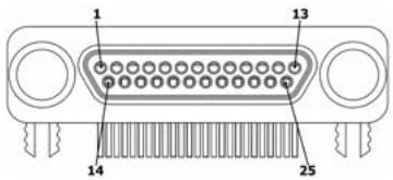
The GPIB connector on PXI-3950 is a micro D-sub 25P connector and is used to control external bench-top instruments. You need the ACL-IEEE488-MD1 cable to connect PXI-3950 and any instruments. The on-board GPIB controller has the following features:

▶ Fully compatible with the IEEE 488 standard
▶ Up to 1.5MB/s data transfer rates
▶ On-board 2 KB FIFO for read/write operations
- Provides driver APIs compatible with NI $^{1}$ -488.2 driver software
▶ Up to 14 instruments may be connected

Figure 2-4: GPIB Connector & Pin Assignments
![1\n13\n14\n25](.pxi-3950-50-17030-1000-003/fb01a13d4976b5c984b82ff0b940ca6032f312b2a739b552a7c6d8a8dee87d40.jpg)

<table><tr><td>PIN</td><td>Signal</td><td>Description</td></tr><tr><td>1</td><td>DIO1#</td><td>GPIB Data 1</td></tr><tr><td>2</td><td>DIO2#</td><td>GPIB Data 2</td></tr><tr><td>3</td><td>DIO3#</td><td>GPIB Data 3</td></tr><tr><td>4</td><td>DIO4#</td><td>GPIB Data 4</td></tr><tr><td>5</td><td>EOI</td><td>End Or Identify</td></tr><tr><td>6</td><td>DAV</td><td>Data Valid</td></tr><tr><td>7</td><td>NRFD</td><td>Not Ready For Data</td></tr><tr><td>8</td><td>NDAC</td><td>Not Data Accepted</td></tr><tr><td>9</td><td>IFC</td><td>Interface Clear</td></tr><tr><td>10</td><td>SRQ</td><td>Service Request</td></tr><tr><td>11</td><td>ATN</td><td>Attention</td></tr><tr><td>12</td><td>Chassis Ground</td><td>Chassis Ground</td></tr><tr><td>13</td><td>Ground</td><td>Signal Ground</td></tr><tr><td>14</td><td>DIO5#</td><td>GPIB Data 5</td></tr><tr><td>15</td><td>DIO6#</td><td>GPIB Data 6</td></tr><tr><td>16</td><td>DIO7#</td><td>GPIB Data 7</td></tr><tr><td>17</td><td>DIO8#</td><td>GPIB Data 8</td></tr><tr><td>18</td><td>REN</td><td>Remote Enable</td></tr><tr><td>19</td><td>Ground</td><td>Signal Ground</td></tr><tr><td>20</td><td>Ground</td><td>Signal Ground</td></tr><tr><td>21</td><td>Ground</td><td>Signal Ground</td></tr><tr><td>22</td><td>Ground</td><td>Signal Ground</td></tr><tr><td>23</td><td>Ground</td><td>Signal Ground</td></tr><tr><td>24</td><td>Ground</td><td>Signal Ground</td></tr><tr><td>25</td><td>Ground</td><td>Signal Ground</td></tr></table>

1. NI is a registered trademark of National Instruments Corporation

# 2.2.4 Reset Button

The reset button is used to perform hard reset for PXI-3950. You can use a pin-like object to push the reset button.

# 2.2.5 LED Indicators

There are four LED indicators on the faceplate to indicate the operating status of the PXI-3950. The following table describes the color and function of the LED indicators.

<table><tr><td>LED Indicator</td><td>Color</td><td>Description</td></tr><tr><td>Power LED</td><td>Green</td><td>Indicates system power status. If the LED is on, the system boots up normally and the main power supply is good.</td></tr><tr><td>HDD LED</td><td>Yellow</td><td>Indicates operating state of the HDD. When the SATA hard drive or CF card is active, the LED indicator flashes.</td></tr><tr><td>Watchdog</td><td>Red</td><td>Indicates status of the watchdog timer. When watchdog timer expires, the LED is on. Please refer to Appendix B for watchdog timer programming information.</td></tr><tr><td>HS LED</td><td>Blue</td><td>Indicates system status. If the system status is good, the LED is on and then off during system boot-up. If the LED keeps blinking or stays on, the system is malfunctioning.Note: If you encounter any malfunction, clear the CMOS (refer to section 2.4.1) and reboot the system. If the system does not respond properly, please contact ADLINK for assistance.</td></tr></table>

Table 2-2: LED Indicators

# 2.2.6 COM Ports

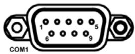
The PXI-3950 provides two COM ports on the faceplate in D-sub 9P connectors. These two serial ports are 16C550 UART compatible and support RS-232/RS-422/RS-485 by jumper selection. Please refer to section 2.4.2 for setting the COM ports.

Figure 2-5: COM Ports & Pin Assignments
![COM1\n1\n6\n5\n9](.pxi-3950-50-17030-1000-003/54e1f0c36189c7b9d0a9fa74ebb435f8f6090dc80285c7fb07e21e568a9f452e.jpg)

![COM2\n1\n6\n5\n9](.pxi-3950-50-17030-1000-003/ceb0a3d55555917440318f72c0887a3274a99445e73c2235ee950715fbe67884.jpg)

<table><tr><td rowspan="2">PIN</td><td colspan="3">Signal Name</td></tr><tr><td>RS-232</td><td>RS-422</td><td>RS-485</td></tr><tr><td>1</td><td>DCD#</td><td>TXD422-</td><td>485DATA-</td></tr><tr><td>2</td><td>RXD#</td><td>TXD422+</td><td>485DATA+</td></tr><tr><td>3</td><td>TXD#</td><td>RXD422+</td><td></td></tr><tr><td>4</td><td>DTR#</td><td>RXD422-</td><td></td></tr><tr><td>5</td><td>GND</td><td></td><td></td></tr><tr><td>6</td><td>DSR#</td><td></td><td></td></tr><tr><td>7</td><td>RTS#</td><td></td><td></td></tr><tr><td>8</td><td>CTS#</td><td></td><td></td></tr><tr><td>9</td><td>RI#</td><td></td><td></td></tr></table>

# 2.2.7 USB 2.0 Ports

The PXI-3950 provides four USB 2.0 ports via Type A USB connectors on the faceplate. All USB ports are compatible with high-speed, full-speed, and low-speed USB devices. The PXI-3950 controller supports multiple boot devices, including USB flash drive, USB floppy, USB CD-ROM, etc. The boot priority and boot device can be configured in BIOS (see section 3.8 for details).

Figure 2-6: USB 2.0 Ports & Pin Assignments
![Pure electrical connector pinout diagram without any text or symbols](.pxi-3950-50-17030-1000-003/c12dc49025c00c2a6303a6333f49c9a4f7f1ca8d4c888fa8ec114de176b8c77b.jpg)

<table><tr><td>PIN</td><td>Signal</td></tr><tr><td>1/5</td><td>Power 5V</td></tr><tr><td>2/6</td><td>USB Data-</td></tr><tr><td>3/7</td><td>USB Data +</td></tr><tr><td>4/8</td><td>Ground</td></tr></table>

![1\n2\n3\n4](.pxi-3950-50-17030-1000-003/cec6e6b915a51a8d6a2bd700d77f97058fe360df292641338daa78ca6cd2d9a7.jpg)

Additionally, the PXI-3950 is shipped with a USB-to-PS2 cable for users who need to connect a PS/2 keyboard and mouse.

Figure 2-7: USB-to-PS/2 Cable
![Coiled electronic device with three colored connectors (green, purple, teal) connected at a junction point (no text or symbols visible)](.pxi-3950-50-17030-1000-003/23c4ae7618f713e80651bac9ed6229a066bf111421622036c4cca4d8243f2980.jpg)

# 2.2.8 Gigabit Ethernet Port

The PXI-3950 has one GbE port from an Intel ICH8M MAC/Intel 82566 PHY and one GbE port from a Marvell 88E8053 Gigabit Ethernet controller via an x1 PCI Express interface to provide dual Gigabit Ethernet connectivity.

The Ethernet controller supports the following features:

▶ x1 PCI Express interface with 2.5 GHz signaling
▶ Advanced error reporting
▶ Message signaled interrupts
▶ TCP segmentation off load/large-send support
▶ 802.3x flow control-compliant
▶ IEEE 802.1p and 802.1q support
▶ 10/100/1000 IEEE 802.3-compliant
▶ Automatic MDI/MDIX crossover at all speeds
▶ ACPI 2.0 specification
▶ Wake-On-Link feature
▶ Fully integrated ASF 2.0 functionality with on-chip $\mu$ c
▶ SMBus 2.0 master interface for ASF functionality
▶ Serial Peripheral Interface (SPI) for ASF firmware and for

Figure 2-8: Gigabit Ethernet Port & Pin Assignments
![LED\nGREEN/ORANGE\nLED YELLOW\n8\n1](.pxi-3950-50-17030-1000-003/95d09712ea4c5991810d6d8206929ef0320ac37624e0ac3c0c96ed0fe6bd21f4.jpg)

<table><tr><td>PIN</td><td>1000Base-T Signal</td><td>100/10Base-T Signal</td></tr><tr><td>1</td><td>MDI0+</td><td>TX+</td></tr><tr><td>2</td><td>MDI0-</td><td>TX-</td></tr><tr><td>3</td><td>MDI1+</td><td>RX+</td></tr><tr><td>4</td><td>MDI2+</td><td>Reserve</td></tr><tr><td>5</td><td>MDI2-</td><td>Reserve</td></tr><tr><td>6</td><td>MDI1-</td><td>RX-</td></tr><tr><td>7</td><td>MDI3+</td><td>Reserve</td></tr><tr><td>8</td><td>MDI3-</td><td>Reserve</td></tr></table>

<table><tr><td colspan="3">Active/Link LED</td></tr><tr><td>LED Color</td><td>Status</td><td>Description</td></tr><tr><td rowspan="3">Yellow</td><td>Off</td><td>Ethernet port is disconnected</td></tr><tr><td>ON</td><td>Ethernet port is connected with no data transmission</td></tr><tr><td>Flash</td><td>Ethernet port is connected and is transmitting/receiving data.</td></tr><tr><td colspan="3">Speed LED</td></tr><tr><td>LED Color</td><td>Status</td><td>Description</td></tr><tr><td rowspan="3">Green/Orange</td><td>Off</td><td>10 Mbps</td></tr><tr><td>Green</td><td>100 Mbps</td></tr><tr><td>Orange</td><td>1000 Mbps</td></tr></table>

Table 2-3: Gigabit Ethernet LED Status Description

# 2.2.9 High Definition Audio Ports

The PXI-3950 implements Intel High Definition audio using the Realtek ALC260/262 chip. The HD audio supports up to 24-bit, 192 Kbps high quality headphone/speaker output and line input. The audio jacks can be accessed on the faceplate of the PXI-3950.

Figure 2-9: High Definition Audio Ports
![ADLINK\nTECHNOLOGY INC.\nWD HO\nPW HS\nTRIG\n1001\n1001\nLine Out\nLine In/MIC In\nPXI-3950](.pxi-3950-50-17030-1000-003/6bc23339aa9ac3c7a34c3ddf2e450dadb924e83dc8a5f443b70349bcf7b9aa03.jpg)

# 2.3 On-board Connectors Layout

Figure 2-10: PXI-3950 Board Layout
![PXI J2\nPXI J1\nCF Socket\nSATA Gen 1 Port](.pxi-3950-50-17030-1000-003/358bc2b54d053aa18a5498bb478d94f905817b0e2740a07a219959dc0aa0a89c.jpg)

# 2.3.1 CompactFlash Socket

The PXI-3950 is equipped with a type II CompactFlash socket which is located on the first layer of the PCB (under the CPU core module). The CF interface supports both ATA and PIO modes. You can use a CF card as replacement of hard drive for better shock/vibration resistance.

Figure 2-11: CompactFlash Socket & Pin Assignments
![Pure electrical circuit lines without any symbols](.pxi-3950-50-17030-1000-003/06825944b0ab754e9238f1584a31b2f671e19827eb900e9fcd7f4b9cdfa6c0d7.jpg)

<table><tr><td>PIN</td><td>SINGAL</td><td>PIN</td><td>SIGNAL</td></tr><tr><td>1</td><td>GND</td><td>26</td><td>GND</td></tr><tr><td>2</td><td>D03</td><td>27</td><td>D11</td></tr><tr><td>3</td><td>D04</td><td>28</td><td>D12</td></tr><tr><td>4</td><td>D05</td><td>29</td><td>D13</td></tr><tr><td>5</td><td>D06</td><td>30</td><td>D14</td></tr><tr><td>6</td><td>D07</td><td>31</td><td>D15</td></tr><tr><td>7</td><td>CS1#</td><td>32</td><td>CS3#</td></tr><tr><td>8</td><td>GND</td><td>33</td><td>GND</td></tr><tr><td>9</td><td>GND</td><td>34</td><td>IORDY#</td></tr><tr><td>10</td><td>GND</td><td>35</td><td>IOWR#</td></tr><tr><td>11</td><td>GND</td><td>36</td><td>WE#</td></tr><tr><td>12</td><td>GND</td><td>37</td><td>INTRQ</td></tr><tr><td>13</td><td>VCC</td><td>38</td><td>VCC</td></tr><tr><td>14</td><td>GND</td><td>39</td><td>CSEL#</td></tr><tr><td>15</td><td>GND</td><td>40</td><td>NC</td></tr><tr><td>16</td><td>GND</td><td>41</td><td>RESET#</td></tr><tr><td>17</td><td>GND</td><td>42</td><td>IORDY</td></tr><tr><td>18</td><td>A02</td><td>43</td><td>DMARQ</td></tr><tr><td>19</td><td>A01</td><td>44</td><td>DMACK#</td></tr><tr><td>20</td><td>A00</td><td>45</td><td>DASP#</td></tr><tr><td>21</td><td>D00</td><td>46</td><td>PDIAG#</td></tr><tr><td>22</td><td>D01</td><td>47</td><td>D08</td></tr><tr><td>23</td><td>D02</td><td>48</td><td>D09</td></tr><tr><td>24</td><td>IOCS16#</td><td>49</td><td>D10</td></tr><tr><td>25</td><td>GND</td><td>50</td><td>GND</td></tr></table>

# 2.3.2 SATA Port

The PXI-3950 provides a SATA Gen. 1 port and is shipped with a pre-installed 2.5" SATA hard drive. The SATA host controller supports two modes of operation, the legacy mode using I/O space and AHCI mode using memory space. You can also use a 2.5" solid state disk (SSD) as a replacement SATA hard drive for shock/vibration resistance.

Figure 2-12: SATA Gen. 1 Port & Pin Assignments
![Pure electrical connector diagram without any text, numbers, or symbols](.pxi-3950-50-17030-1000-003/8e2078ace93ecc1e20c1a688e7d05518ced33f1f10363cd67555ba17297046a9.jpg)

<table><tr><td>Signal</td><td>PIN</td><td>PIN</td><td>Signal</td></tr><tr><td>GND</td><td>1</td><td>2</td><td>GND</td></tr><tr><td>Reserve</td><td>3</td><td>4</td><td>Reserve</td></tr><tr><td>Reserve</td><td>5</td><td>6</td><td>Reserve</td></tr><tr><td>Reserve</td><td>7</td><td>8</td><td>Reserve</td></tr><tr><td>Reserve</td><td>9</td><td>10</td><td>Reserve</td></tr><tr><td>Reserve</td><td>11</td><td>12</td><td>Reserve</td></tr><tr><td>Reserve</td><td>13</td><td>14</td><td>Reserve</td></tr><tr><td>Reserve</td><td>15</td><td>16</td><td>Reserve</td></tr><tr><td>Reserve</td><td>17</td><td>18</td><td>Reserve</td></tr><tr><td>Reserve</td><td>19</td><td>20</td><td>GND</td></tr><tr><td>GND</td><td>21</td><td>22</td><td>Reserve</td></tr><tr><td>Reserve</td><td>23</td><td>24</td><td>Reserve</td></tr><tr><td>Reserve</td><td>25</td><td>26</td><td>Reserve</td></tr><tr><td>Reserve</td><td>27</td><td>28</td><td>Reserve</td></tr><tr><td>Reserve</td><td>29</td><td>30</td><td>GND</td></tr><tr><td>Reserve</td><td>31</td><td>32</td><td>+5V</td></tr><tr><td>Reserve</td><td>33</td><td>34</td><td>+5V</td></tr><tr><td>Reserve</td><td>35</td><td>36</td><td>+5V</td></tr><tr><td>Reserve</td><td>37</td><td>38</td><td>+12V</td></tr><tr><td>Reserve</td><td>39</td><td>40</td><td>+12V</td></tr><tr><td>Reserve</td><td>41</td><td>42</td><td>+12V</td></tr><tr><td>GND</td><td>43</td><td>44</td><td>GND</td></tr><tr><td>SATA_RXn</td><td>45</td><td>46</td><td>SATA_TXn</td></tr><tr><td>SATA_RXp</td><td>47</td><td>48</td><td>SATA_TXp</td></tr><tr><td>GND</td><td>49</td><td>50</td><td>GND</td></tr></table>

# 2.3.3 PXI J1

Figure 2-13: J1 Connector & Pin Assignments
![25\n15\n11\n1\ne\nd\nc\nb\na](.pxi-3950-50-17030-1000-003/7c51aa147f315c5f78b9e6c5ab9838a5cdc27ad91a880dc830fcf7ea5f321b51.jpg)

<table><tr><td>Pin</td><td>Z</td><td>A</td><td>B</td><td>C</td><td>D</td><td>E</td><td>G</td></tr><tr><td>J1-25</td><td>GND</td><td>+5V</td><td>REQ64#</td><td>ENUM#</td><td>+3.3V</td><td>+5V</td><td>GND</td></tr><tr><td>J1-24</td><td>GND</td><td>AD[1]</td><td>+5V</td><td>V(I/O)</td><td>AD[0]</td><td>ACK64#</td><td>GND</td></tr><tr><td>J1-23</td><td>GND</td><td>+3.3V</td><td>AD[4]</td><td>AD[3]</td><td>+5V</td><td>AD[2]</td><td>GND</td></tr><tr><td>J1-22</td><td>GND</td><td>AD[7]</td><td>GND</td><td>+3.3V</td><td>AD[6]</td><td>AD[5]</td><td>GND</td></tr><tr><td>J1-21</td><td>GND</td><td>+3.3V</td><td>AD[9]</td><td>AD[8]</td><td>M66EN</td><td>C/BE[0]#</td><td>GND</td></tr><tr><td>J1-20</td><td>GND</td><td>AD[12]</td><td>GND</td><td>V(I/O)</td><td>AD[11]</td><td>AD[10]</td><td>GND</td></tr><tr><td>J1-19</td><td>GND</td><td>+3.3V</td><td>AD[15]</td><td>AD[14]</td><td>GND</td><td>AD[13]</td><td>GND</td></tr><tr><td>J1-18</td><td>GND</td><td>SERR#</td><td>GND</td><td>+3.3 V</td><td>PAR</td><td>C/BE[1]#</td><td>GND</td></tr><tr><td>J1-17</td><td>GND</td><td>+3.3V</td><td>NC</td><td>NC</td><td>GND</td><td>PERR#</td><td>GND</td></tr><tr><td>J1-16</td><td>GND</td><td>DEVSEL#</td><td>GND</td><td>V(I/O)</td><td>STOP#</td><td>LOCK#</td><td>GND</td></tr><tr><td>J1-15</td><td>GND</td><td>+3.3V</td><td>FRAME#</td><td>IRDY#</td><td>GND</td><td>TRDY#</td><td>GND</td></tr><tr><td>J1-12~14</td><td>GND</td><td colspan="6"></td></tr><tr><td>J1-11</td><td>GND</td><td>AD[18]</td><td>AD[17]</td><td>AD[16]</td><td>GND</td><td>C/BE[2]#</td><td>GND</td></tr><tr><td>J1-10</td><td>GND</td><td>AD[21]</td><td>GND</td><td>+3.3V</td><td>AD[20]</td><td>AD[19]</td><td>GND</td></tr><tr><td>J1-9</td><td>GND</td><td>C/BE[3]#</td><td>GND</td><td>AD[23]</td><td>GND</td><td>AD[22]</td><td>GND</td></tr><tr><td>J1-8</td><td>GND</td><td>AD[26]</td><td>GND</td><td>V(I/O)</td><td>AD[25]</td><td>AD[24]</td><td>GND</td></tr><tr><td>J1-7</td><td>GND</td><td>AD[30]</td><td>AD[29]</td><td>AD[28]</td><td>GND</td><td>AD[27]</td><td>GND</td></tr><tr><td>J1-6</td><td>GND</td><td>REQ0#</td><td>GND</td><td>+3.3V</td><td>CLK0</td><td>AD[31]</td><td>GND</td></tr><tr><td>J1-5</td><td>GND</td><td>NC</td><td>NC</td><td>RST#</td><td>GND</td><td>GNT0#</td><td>GND</td></tr><tr><td>J1-4</td><td>GND</td><td>NC</td><td>HEALTHY#</td><td>V(I/O)</td><td>INTP</td><td>INTS</td><td>GND</td></tr><tr><td>J1-3</td><td>GND</td><td>INTA#</td><td>INTB#</td><td>INTC#</td><td>+5V</td><td>INTD#</td><td>GND</td></tr><tr><td>J1-2</td><td>GND</td><td>TCK</td><td>+5V</td><td>TMS</td><td>TDO</td><td>TDI</td><td>GND</td></tr><tr><td>J1-1</td><td>GND</td><td>+5V</td><td>-12V</td><td>TRST#</td><td>+12V</td><td>+5V</td><td>GND</td></tr><tr><td>Pin</td><td>Z</td><td>A</td><td>B</td><td>C</td><td>D</td><td>E</td><td>G</td></tr></table>

# 2.3.4 PXI J2

Figure 2-14: J2 Connector & Pin Assignments
![22\n1\ne\nd\nc\nb\na](.pxi-3950-50-17030-1000-003/501de230d8bd223d1858f30910e75296ea78ed192b777fc4d99e65a106ca6db5.jpg)

<table><tr><td>Pin</td><td>Z</td><td>A</td><td>B</td><td>C</td><td>D</td><td>E</td><td>G</td></tr><tr><td>J1-22</td><td>GND</td><td>NC (GA4)</td><td>NC (GA3)</td><td>NC (GA2)</td><td>NC (GA1)</td><td>NC (GA0)</td><td>GND</td></tr><tr><td>J1-21</td><td>GND</td><td>CLK6</td><td>GND</td><td>NC (RSV)</td><td>RSV</td><td>RSV#</td><td>GND</td></tr><tr><td>J1-20</td><td>GND</td><td>CLK5</td><td>GND</td><td>RSV</td><td>GND</td><td>RSV</td><td>GND</td></tr><tr><td>J1-19</td><td>GND</td><td>GND</td><td>GND</td><td>(SMB_SDA)</td><td>(SMB_SCL)</td><td>(SMB_ALERT#)</td><td>GND</td></tr><tr><td>J1-18</td><td>GND</td><td>PXI_TRIG3</td><td>PXI_TRIG4</td><td>PXI_TRIG5</td><td>GND</td><td>PXI_TRIG6</td><td>GND</td></tr><tr><td>J1-17</td><td>GND</td><td>PXI_TRIG2</td><td>GND</td><td>REST#</td><td>REQ6#</td><td>GNT6#</td><td>GND</td></tr><tr><td>J1-16</td><td>GND</td><td>PXI_TRIG1</td><td>PXI_TRIG0</td><td>DEG#</td><td>GND</td><td>PXI_TRIG7</td><td>GND</td></tr><tr><td>J1-15</td><td>GND</td><td>NC(PXI_BRSVA15)</td><td>GND</td><td>FAL#</td><td>REQ5#</td><td>GNT5#</td><td>GND</td></tr><tr><td>J1-14</td><td>GND</td><td>AD[35]</td><td>AD[34]</td><td>AD[33]</td><td>GND</td><td>AD[32]</td><td>GND</td></tr><tr><td>J1-13</td><td>GND</td><td>AD[38]</td><td>GND</td><td>V(I/O)</td><td>AD[37]</td><td>AD[36]</td><td>GND</td></tr><tr><td>J1-12</td><td>GND</td><td>AD[42]</td><td>AD[41]</td><td>AD[40]</td><td>GND</td><td>AD[39]</td><td>GND</td></tr><tr><td>J1-11</td><td>GND</td><td>AD[45]</td><td>GND</td><td>V(I/O)</td><td>AD[44]</td><td>AD[43]</td><td>GND</td></tr><tr><td>J1-10</td><td>GND</td><td>AD[49]</td><td>AD[48]</td><td>AD[47]</td><td>GND</td><td>AD[46]</td><td>GND</td></tr><tr><td>J1-9</td><td>GND</td><td>AD[52]</td><td>GND</td><td>V(I/O)</td><td>AD[51]</td><td>AD[50]</td><td>GND</td></tr><tr><td>J1-8</td><td>GND</td><td>AD[56]</td><td>AD[55]</td><td>AD[54]</td><td>GND</td><td>AD[53]</td><td>GND</td></tr><tr><td>J1-7</td><td>GND</td><td>AD[59]</td><td>GND</td><td>V(I/O)</td><td>AD[58]</td><td>AD[57]</td><td>GND</td></tr><tr><td>J1-6</td><td>GND</td><td>AD[63]</td><td>AD[62]</td><td>AD[61]</td><td>GND]</td><td>AD[60]</td><td>GND</td></tr><tr><td>J1-5</td><td>GND</td><td>C/BE[5]\#</td><td>GND</td><td>V(I/O)</td><td>C/BE[4]\#</td><td>PAR64</td><td>GND</td></tr><tr><td>J1-4</td><td>GND</td><td>V(I/O)</td><td>NC(PXI_BRSVB4)</td><td>C/BE[7]\#</td><td>GND</td><td>C/BE[6]\#</td><td>GND</td></tr><tr><td>J1-3</td><td>GND</td><td>CLK4</td><td>GND</td><td>GNT3#</td><td>REQ4#</td><td>GNT4#</td><td>GND</td></tr><tr><td>J1-2</td><td>GND</td><td>CLK2</td><td>CLK3</td><td>SYSEN#</td><td>GNT2#</td><td>REQ3#</td><td>GND</td></tr><tr><td>J1-1</td><td>GND</td><td>CLK1</td><td>GND</td><td>REQ1#</td><td>GNT1#</td><td>REQ2#</td><td>GND</td></tr><tr><td>Pin</td><td>Z</td><td>A</td><td>B</td><td>C</td><td>D</td><td>E</td><td>G</td></tr></table>

# 2.4 Jumper Layout

Figure 2-15: PXI-3950 Jumper Layout
![Clear CMOS\nJP9\nJP2 JP4 JP6\nJP1 JP3 JP5\nCOM2 Jumpers\nCOM1 Jumpers](.pxi-3950-50-17030-1000-003/88ec2f27aca422095bc875827685ad3a9d291db600c9718809bbf5ecdfe7dee3.jpg)

# 2.4.1 Clear CMOS (JP9)

If you encounter an abnormal condition that causes PXI-3950 to halt or fail to boot, clear the CMOS and restore the controller BIOS to its default settings. To clear the CMOS, locate the JP9 jumper on the board and short pin#2 and pin#3. After you have cleared the COMS, restore the jumper by returning to normal mode (short pin#1 and pin#2).

Figure 2-16: JP9 (Clear CMOS) Settings

<table><tr><td>Normal</td><td>Clear</td></tr><tr><td>JP9
1
2
3</td><td>JP9
1
2
3</td></tr></table>

# 2.4.2 COM1/COM2 Mode Settings (JP1/JP2/JP3/JP4/JP5/JP6)

COM1 and COM2 on PXI-3950 controllers support RS-232, RS-422, and RS-485 specifications. JP1, JP2, JP3, JP4, JP5, and JP6 are used set the operation mode of COM1 and COM2. Please refer to the following table for mode settings.

Figure 2-17: COM1 & COM2 JP1 through JP6 Settings
![COM1\nRS-232 RS-422 RS-485\nJP1 JP1 JP1 JP2 JP2 JP2\n1 2 1 2 1 2 1 2 1 2 1 2\n3 4 3 4 3 4 3 4 3 4\n5 6 5 6 5 6 5 6 5 6 5 6\nJP3 JP3 JP3 JP4 JP4 JP4\n1 2 1 2 1 2 1 2 1 2 1 2\n3 4 3 4 3 4 3 4 3 4\n5 6 5 6 5 6 5 6 5 6 5 6\nJP5 JP5 JP5 JP6 JP6 JP6\n1 2 1 2 1 2 1 2 1 2\n3 4 3 4 3 4 3 4 3 4\n5 6 5 6 5 6 5 6 5 6\nCOM2\nRS-422 RS-485\nJP1 JP1 JP2 JP2 JP2\n1 2 1 2 1 2 1 2 1 2\n3 4 3 4 3 4 3 4\n5 6 5 6 5 6 5 6\nJP3 JP3 JP4 JP4 JP4\n1 2 1 2 1 2 1 2 1 2\n3 4 3 4 3 4 3 4\n5 6 5 6 5 6 5 6\nJP5 JP5 JP6 JP6 JP6\n1 2\n3 4\n5 6\n5.6](.pxi-3950-50-17030-1000-003/9872e86368cba455fcf292f5fee2792f2876c3ce6b49277a43bf9a922589e8f1.jpg)

# 3 Getting Started

This chapter gives the illustration of how to install the PXI-3950 into your PXI system. Additional hardware installation and BIOS setup are also described. Please note that the PXI-3950 is shipped with CPU, RAM and HDD preinstalled. The procedures of installing the operating system and booting from a USB or CF device are also illustrated. Please contact ADLINK or our authorized dealer if you meet any problem during the installation.

# 3.1 Installation Environment

Whenever unpacking and preparing to install any equipment described in this manual, please refer to the Important Safety Instructions chapter of this manual.

Only install equipment in well lit areas on flat, sturdy surfaces with access to basic tools such as flat and cross head screwdrivers, preferably with magnetic heads as screws and standoffs are small and easily misplaced.

# Recommended Installation Tools

▶ Phillips (cross-head) screwdriver
▶ Flat-head screwdriver
Anti-static Wrist Strap
Anti-static mat

ADLINK PXI-3950 System Controllers are electro-static sensitive equipment that can be easily damaged by static electricity. The equipment must be handled on a grounded anti-static mat. The operator must wear an anti-static wristband, grounded at the same point as the anti-static mat.

Inspect the carton and packaging for damage. Shipping and handling could cause damage to the equipment inside. Make sure that the equipment and its associated components have no damage before installing.

![This image features a triangular warning sign with a yellow background and a thick black border. Centered inside the triangle is a large black exclamation point. Below the triangle, the word 'CAUTION:' is printed in black capital letters.](.pxi-3950-50-17030-1000-003/2cb717e9cd23712951cd704f6e3d73f47ce49e9ba27ce7637e2b60bc418c6172.jpg)

The equipment must be protected from static discharge and physical shock. Never remove any of the socketed parts except at a static-free workstation. Use the anti-static bag shipped with the product to handle the equipment and wear a grounded wrist strap when servicing.

# 3.1.1 Compatible Chassis

The PXI-3950 implements rear I/O functions for inter-chassis signal transmissions. Before installing the PXI-3950, please make sure your PXI chassis is compatible with PXI-3950. You can use the following PXI chassis with PXI-3950.

ADLINK PXIS-2506
ADLINK PXIS-2508
▶ ADLINK PXIS-2558T-B (supports rear I/O for PXI-3920/3910/3950)
ADLINK PXIS-2630
ADLINK PXIS-2670
ADLINK PXIS-2700
ADLINK PXIS-2719
ADLINK PXIS-2690P-B (supports rear I/O for PXI-3920/3910/3950)
▶ Any National Instruments $^{1}$ PXI chassis

![The image displays a yellow triangular warning sign with a black border. Centered inside the triangle is a large black exclamation mark. Below the triangle, on a white background, the text 'CAUTION:' is printed in black capital letters.](.pxi-3950-50-17030-1000-003/e66fa185ad808c3278512af36bc156f042c26f76f6b96bcecd63499e14c99f76.jpg)

DO NOT install PXI-3950 in the following PXI chassis:

ADLINK PXIS-2556/2556T

ADLINK PXIS-2558T-A

ADLINK PXIS-2650/2650T

ADLINK PXIS-2680P

ADLINK PXIS-2690P

1. National Instruments is a registered trademark of National Instruments Corporation

# 3.2 Installing PXI-3950

# 1. Locate the system controller slot (Slot 1)

![ADLINK\nPXi](.pxi-3950-50-17030-1000-003/39d5e5426c103a4eb0484405288bdf076599521ccdf6a566798a09c5886f6d24.jpg)

2. Push down (loosen) the ejector/injector handle of the PXI-3950 controller.
3. Align the controller's top and bottom edges to the card guides, then carefully slide the PXI-3950 into the chassis.

![Close-up of an ADLINK industrial control module with visible wiring and ports, no readable text or symbols on the main components.](.pxi-3950-50-17030-1000-003/9d877bd7dd2905eea4e71de98ec8a96a1794dfc2215cfae007b5ca7fc58c87be.jpg)

4. Pull up the ejector/injector handle until the PXI-3950 is properly connected to the chassis backplane.

![Front view of an ADLINK industrial control module with visible ports, connectors, and a central rack (no readable text or symbols)](.pxi-3950-50-17030-1000-003/2baaa9cd01575cd76cab8a5daa482650ceb55b1f5f1ce6a24e17ed9e9fbdc942.jpg)

5. Fasten the screws on the faceplate of PXI-3950, and then connect all peripheral devices to the PXI-3950 controller.

![ADLINK\nADLINK\nFXI-3550\nFXi](.pxi-3950-50-17030-1000-003/008ecc8107d51eb87bc1cefbefef606b693507a2c17f92defbc40ef043a71cf5.jpg)

# 3.3 Hard Drive Replacement

By default, the PXI-3950 PXI controller is shipped with a 2.5" 120 GB SATA hard drive pre-installed. For users who need to change the SATA hard drive or use a solid state disk (SSD) as the replacement hard drive, please follow the instructions below.

1. The hard drive is located on the back side of the PXI-3950 controller. Locate the four screws that attach the hard drive to the bracket.

![Internal view of a computer hard drive module with visible circuitry and connectors (no text or symbols)](.pxi-3950-50-17030-1000-003/aaca5833669a439ba067ee1e61aaff3deb161b3f8d04036b98bf2cef86c912c6.jpg)

2. Loosen the screws.

![Close-up of an electronic device showing a hard disk with attached circuit board and cooling fan (no visible text or symbols)](.pxi-3950-50-17030-1000-003/a16663b23bf477318b810eb7c2e1efb698d0d370c800e5a2646949553b66236e.jpg)

3. Gently pull out the SATA hard drive. Be careful not to bend or break the SATA Board-to-Board connector.

![Close-up of a green computer motherboard with visible drive bays and connectors (no readable text or symbols)](.pxi-3950-50-17030-1000-003/11e63a4f42578be19a7d7a8498cf861fb5cced2b01d31194e599a29718d12f97.jpg)

4. To replace the HD with your choice of solid state hard drive or other compatible SATA hard drive, follow the revers steps, and re-install the PXI-3950 to your PXI system.

![Top-down view of a green computer motherboard with visible components and connectors (no text or symbols)](.pxi-3950-50-17030-1000-003/90d988d163dd637cd4b4cb4cfc977dfcc922b3f5a4e65df79b21a0579a1bf2d3.jpg)

# 3.4 CompactFlash Card Installation

The PXI-3950 provides a CompactFlash Type II socket to accommodate a CF card as a replacement hard drive. You can also install a SATA hard drive and CF card simultaneously and set the boot device preferences in BIOS (refer to section 3.6 for details). Please follow the instructions below to install the CF card.

1. Locate the CompactFlash socket. The socket is located under the SATA hard drive.

![Internal view of a computer motherboard with a red arrow pointing to a component, showing no visible text or symbols.](.pxi-3950-50-17030-1000-003/cadb4fccb82934fd279258b68ebeb61a128c48411611d87fbcef646334379a34.jpg)

2. Insert the CF card and press down to make sure it is firmly attached in its socket.

![Interior view of a computer motherboard showing internal components and a red arrow pointing to a component labeled 'Z6B' (no readable text beyond label)](.pxi-3950-50-17030-1000-003/9a669474874a7740f44fd27e75f346e55ef3a9a21578ada0b65a131471a5098d.jpg)

# 3.5 BIOS Configuration

The Basic Input/Output System (BIOS) is a program that provides a basic level of communication between the processor and peripherals. In addition, the BIOS also contain code for various advanced features applied to the PXI-3950 controller. The BIOS setup program includes menus for configuring settings and enabling PXI-3950 controller features. Most users do not need to use the BIOS setup program, as the PXI-3950 controller ships with default settings that work well for most configurations.

![The image shows a yellow triangular warning sign with a black exclamation mark in the center. Below the triangle, the word 'CAUTION:' is printed in black capital letters.](.pxi-3950-50-17030-1000-003/f7e0fce964a0f6f316eec61bf477c440fe8ac60c087b31e738fa7d36df983bb2.jpg)

Changing BIOS settings may lead to incorrect controller behavior and possibly an unbootable controller. If this happens, follow the instructions in section 2.4.1 to clear CMOS and then restore the default settings. In general, do not change a BIOS setting unless you are absolutely certain of what it does.

# 3.6 Operating System Installation

For more detailed information about the operating system, refer to the documentation provided by the operating system vendor. The preferred/supported operating systems for PXI-3950 are:

▶ Windows 2000
▶ Windows XP
▶ Windows Vista
▶ For other OS support, please contact ADLINK

Most operating systems require initial installation on a hard drive, floppy drive, or a CD-ROM drive. The PXI-3950 controller supports USB CD-ROM drive, USB flash disk, USB external hard drive, or a USB floppy drive as the first boot device. Please refer to section 3.8 for information about setting the boot devices. These devices should be configured, installed, and tested with the supplied drivers before attempting to load the new operating system.

![The image features a graphic icon of a white sheet of paper with faint horizontal lines and a folded top-left corner. A large, bold red checkmark is drawn diagonally across the document.](.pxi-3950-50-17030-1000-003/6f3bd22a234012951cbab24d2d89571e03922f865a13d5499ddaad791365e831.jpg)
NOTE:

Read the release notes and installation documentation provided by the operating system vendor. Be sure to read all the README files or documents provided on the distribution disks, as these typically note documentation discrepancies or compatibility problems.

Select the appropriate boot device order in the SETUP/BIOS boot menu depending on the OS installation media used. For example, if the OS is distributed with a bootable installation CD, select USB CD-ROM as the first boot device and reboot the system with the installation CD installed in the USB CD-ROM drive.

Proceed with the OS installation as directed and be sure to select appropriate device types if prompted. Refer to the appropriate hardware manuals for specific device types and compatibility modes of ADLINK PXI products.

When installation is complete, reboot the system and set the boot device order in the SETUP boot menu appropriately.

# 3.7 Setting PXI-3950 Boot Devices

The PXI-3950 controller by default boots up from the SATA hard drive. However, you can also set a USB device or a CF card as the boot device in BIOS. Please follow the instructions below to set the boot device of PXI-3950.

# Boot from SATA hard drive

▶ Make sure the bootable SATA hard drive is installed in the hard drive bracket.
▶ Power on the PXI-3950 and enter BIOS to modify the setting of boot device as following:

▷ [Boot] » [Hard Disk Drives] » [1st Drive]

![The image displays a white document icon with a folded upper-right corner and horizontal lines indicating text. A large, red checkmark is drawn diagonally across the center of the document.](.pxi-3950-50-17030-1000-003/88304efb1aa5a076516d5a7b5b7f0af1e8a942d2af3c9c31bc7f0d137e012aaa.jpg)
NOTE:

If there is a CF card installed, you will see 1st Drive and 2nd Drive shown. Please recognize the bootable SATA hard drive according the model name comes after the xth Drive on the screen and set it to 1st Drive.

▷ [Boot] » [1st Boot Device] » [SATA:XX]

![The image displays an icon of a white document or page with a folded top-right corner and faint horizontal lines, overlaid with a large red checkmark.](.pxi-3950-50-17030-1000-003/b3ef332f5fe7b17361bb65e35939550cd7926e00d0e7acbe1c1ec09cd33c3636.jpg)
NOTE:

"SATA:XX" refers to the model name selected in last step.

▶ Save the change
▶ Reboot the system

# Boot from on-board CF card

▶ Make sure the bootable CF is firmly installed in the CF socket.
▶ Power on the PXI-3950 and enter BIOS to modify the setting of boot device as following:
▷ [Boot] » [Hard Disk Drives] » [1st Drive]

![The image displays a white document icon with a folded top-right corner and faint horizontal gray lines. Superimposed over the center is a large, bold red checkmark.](.pxi-3950-50-17030-1000-003/343d07964d5a6b84f73b93f4c5765145fec1ecbdc249004cf33290f0829f2c03.jpg)
NOTE:

If there is a hard drive installed, you will see 1st Drive and 2nd Drive shown. Please recognize the bootable CF according the model name comes after the xth Drive on the screen and set it to 1st Drive.

▷ [Boot] » [1st Boot Device] » [HDD:XX]

![The image displays a digital icon featuring a white piece of paper or document. The top-left corner of the paper is folded down (a 'dog-ear'). Faint, gray horizontal lines run across the lower portion of the document, suggesting a form or text area. A large, bold red checkmark (or tick) is superimposed over the center of the paper, slanting upwards from left to right.](.pxi-3950-50-17030-1000-003/6b56e17a680ee4242dac1adba9558d48b97150d30a2692cdf1ca9a8125c37886.jpg)
NOTE:

"HDD:XX" refers to the model name selected in last step.

▶ Save the change
▶ Reboot the system

# Boot from USB CD-ROM drive

- Connect the USB CD-ROM drive via a USB port on the faceplate.
▶ Put a bootable CD in the USB CD-ROM Drive.
▶ Power on the PXI-3950 and enter BIOS to modify the setting of boot device as following:
▷ [Boot] » [USB Drives] » [1st Drive]

![The image displays an icon of a white document with faint horizontal lines and a folded top-left corner. A large red checkmark is superimposed over the document.](.pxi-3950-50-17030-1000-003/30d88608b1cb15452213ba1c7298e04ad9813449fa802030054c69daeeb2e940.jpg)
NOTE:

If there are multiple USB external devices installed, you will see 1st Drive, 2nd Drive and etc. Please recognize the USB CD-ROM according the model name comes after the xth Drive on the screen and set it to 1st Drive.

▷ [Boot] » [1st Boot Device] » [USB:XX]

![The image displays a white piece of paper with horizontal lines and a folded top-right corner, resembling a form or document. A large red checkmark is drawn over the left side of the paper.](.pxi-3950-50-17030-1000-003/df63a5508b2ac5ac9199090a9949d312cd7defb93f35e25a1067f9b8c6a29589.jpg)
NOTE:

"USB:XX" refers to the model name selected in last step.

▶ Save the change
▶ Reboot the system

# Boot from USB Flash disk

- Connect a bootable USB Flash disk via a USB port on the faceplate.
▶ Power on the PXI-3950 and enter BIOS to modify the setting of boot device as following:

▷ [Boot] » [USB Drives] » [1st Drive]

![The image displays a digital icon representing a document or checklist. It features a white sheet of paper with the top-left corner folded. Faint horizontal lines run across the surface of the paper. A large, bold red checkmark is superimposed over the center of the document. There is no text present.](.pxi-3950-50-17030-1000-003/e203a1e28761a8a3d64676b09267e67d6c9e72bf906f5c31bb3ddc9e305e43e1.jpg)
NOTE:

If there are multiple USB external devices installed, you will see 1st Drive, 2nd Drive and etc. Please recognize the USB Flash disk according the model name comes after the xth Drive on the screen and set it to 1st Drive.

▷ [Boot] » [1st Boot Device] » [USB:XX]

![The image displays a white document icon featuring faint horizontal lines, with a large red checkmark superimposed over it.](.pxi-3950-50-17030-1000-003/c28fcd0d80309267f8c6fea5183bf3419d5fc9a7d824c3847a75740cfe8b1296.jpg)
NOTE:

"USB:XX" refers to the model name selected in last step.

▶ Save the change
▶ Reboot the system

# Boot from USB external hard drive

▶ Connect a bootable USB external hard drive via a USB port on the faceplate.
▶ Power on the PXI-3950 and enter BIOS to modify the setting of boot device as following:

▷ [Boot] » [USB Drives] » [1st Drive]

![The image displays an icon of a white document with a folded top-right corner and several horizontal lines representing text. Overlaid on the document is a large, red checkmark (or tick).](.pxi-3950-50-17030-1000-003/fe3b908f58ba61c44953373b4e8e2c82f0540c67aa0ba4db14f0eff5ad922c75.jpg)
NOTE:

If there are multiple USB external devices installed, you will see 1st Drive, 2nd Drive and etc. Please recognize the USB external hard drive according to the model name comes after the xth Drive on the screen and set it to 1st Drive.

▷ [Boot] » [1st Boot Device] » [USB:XX]

![The image displays a white document icon with a folded top-right corner and faint horizontal lines. A large, bold red checkmark is superimposed over the center of the document.](.pxi-3950-50-17030-1000-003/e70b13893c32dbc29c4d103997109e4afdba85435a9690fbe9a21b343c9b01a6.jpg)
NOTE:

"USB:XX" refers to the model name selected in last step.

▶ Save the change
▶ Reboot the system

# Boot from USB floppy drive

- Connect the USB floppy drive via a USB port on the faceplate.
▶ Put a bootable disk in the USB floppy drive.
▶ Power on the PXI-3950 and enter BIOS to modify the setting of boot device as following:

▷ [Boot] » [USB Drives] » [1st Drive]

![The image displays an icon of a white document with a folded top-left corner. Faint grey horizontal lines run across the lower portion of the document. A large, bold red checkmark is superimposed on the right side of the paper.](.pxi-3950-50-17030-1000-003/19d97ce86a77c1cac8336767344a92aa4be42358269cc305a195cd20dd1a772c.jpg)
NOTE:

If there are multiple USB external devices installed, you will see 1st Drive, 2nd Drive and etc. Please recognize the USB floppy drive according the model name comes after the xth Drive on the screen and set it to 1st Drive.

▷ [Boot] » [1st Boot Device] » [USB:XX]

![The image displays a graphic of a white document with a folded upper-left corner. Faint horizontal gray lines are visible on the page. A large, red checkmark is superimposed diagonally across the center of the document. There is no text in the image.](.pxi-3950-50-17030-1000-003/2dacc99d8dca1951ec99b22a429552735a7f36576a0cd052f12daf9cf8683fc2.jpg)
NOTE:

"USB:XX" refers to the model name selected in last step.

▶ Save the change
▶ Reboot the system

# 3.8 Using the PXI-3950 with a PXI-2558T-B or PXIS-2690P-B Chassis

This section describes the usage of PXI-3950 controllers in PXI-2558T-B and PXIS-2690P-B chassis. These chassis are unique in that they support a built-in LCD display and warrant special BIOS configurations to properly operate the system controller.

The PXI-3950 controller supports a rear I/O option. The rear I/O option is designed to operate with a matching rear transition module which provides internal chassis I/O, including video signals, USB signals, etc. The ADLINK PXI-2558T-B is a 3U 8-slot PXI chassis with built-in 8.4" LCD touch panel, while the PXIS-2690P-B is a 3U 14-slot portable PXI chassis with built-in 15" LCD touch panel. Both of them contain a matching rear transition module for PXI-3950 to support internal signal transmission.

While installing PXI-3950 in the PXIS-2558T-B or the PXIS-2690P-B chassis, please make sure you have correct BIOS setting to turn on the LCD touch panel by the following steps.

1. Press DEL while booting to enter the BIOS setting screen.
2. Use left and right arrow to enter "Chipset".
3. Set the "Boot Display Device" option as "CRT+LVDS".
4. Set the "Flat Panel Type" as following:

For PXIS-2558T-B, select "800x600 18Bit"

For PXIS-2690P-B, select "1024x768 24Bit"

5. Save your setting and exit the BIOS.

![The image displays a white document icon with a folded top-right corner and faint horizontal lines, overlaid with a large red checkmark.](.pxi-3950-50-17030-1000-003/cf06b729d8837e1fd55bd90836230f43178cf69da058afe8b7d38a25333c2f19.jpg)
NOTE:

Currently PXIS-2558T-B and PXIS-2690P-B are the only PXI chassis with a built-in LCD touch panel which supports PXI-3950 controllers. Please DO NOT install PXI-3950 controllers in other chassis with built-in LCD panel, such as PXIS-2556T, PXIS-2650T, PXIS-2680P, or PXIS-2690P.

This page intentionally left blank.

# 4 Driver Installation

After installing the operating system, you need to install all related drivers to make your system work accordingly. In this section, we describe the drivers needed for Windows operating systems and the procedures to install them. For other OS support, please contact ADLINK for further information.

![The image displays a white document icon with a folded top-left corner and faint horizontal gray lines. A large, bold red checkmark is superimposed on the front of the document.](.pxi-3950-50-17030-1000-003/0f048479e0f385047228752431ef6373f4960e8f583bc1815095da58a15a960e.jpg)
NOTE:

The Windows operating system environment supports a wide array of drivers as it has extended plug and play support. most standard I/O device drivers are automatically included.

# 4.1 Chipset Drivers

This section describes the procedure to install the chipset driver of PXI-3950. The chipset driver outlines to the operating system how to configure the Intel GME965 chipset components in order to ensure that the following features function properly:

▶ Core PCI and ISAPNP Services
▶ PCIe Support
▶ IDE/ATA33/ATA66/ATA100 Storage Support
▶ SATA Storage Support
▶ USB Support
▶ Identification of Intel Chipset Components in the Device Manager

One of the following operating systems must be fully installed and running on the system before installing this software:

▶ Microsoft Windows Server 2003
▶ Microsoft Windows Server 2003 x64 Edition\*
▶ Microsoft Windows XP Professional x64 Edition\*
▶ Microsoft Windows XP
▶ Microsoft Windows 2000
▶ Microsoft windows Vista

Please follow the following steps to install chipset drivers for PXI-3950.

▶ Close any running application.
▶ Insert the ADLINK All-in-One CD. The chipset driver is located in the directory:

```txt
x:\Driver Installation\PXI Platform\PXI controller\PXI-3950\Chipset\2000_XP_Vista\, where x: denotes the CD-ROM drive.
```

▶ Execute Setup.exe and follow on-screen instructions to complete the setup.

▶ Reboot your system.

# 4.2 Graphics Driver

The PXI-3950 controller is equipped with Intel GMA X3100 graphic media accelerator integrated in the Intel GME965 Express Chipset. The Intel Graphics Media Accelerator Driver package supports the following operating systems:

▶ Windows 2000
▶ Windows XP

Please follow the following steps to install graphics drivers for PXI-3950.

▶ Close any running application.
▶ Insert the ADLINK All-in-One CD. The chipset driver is located in the directory:

```txt
x:\Driver Installation\PXI Platform\PXI controller\PXI-3950\VGA\2000_XP\, where x: denotes the CD-ROM drive.
```

▶ Execute Setup.exe and follow on-screen instructions to complete the setup.

▶ Reboot your system.

![The image displays a document icon featuring a white piece of paper with a folded top-right corner and faint horizontal lines. A large, bold red checkmark is superimposed diagonally across the center of the paper.](.pxi-3950-50-17030-1000-003/f5bf9909ee175bb35652bf6f5b733f105bf3d5a6eca62b3560390e3b624180e0.jpg)
NOTE:

If you use PXI-3950 with ADLINK PXIS-2558T-B or PXIS-2690P chassis, please set the graphic output as "Dual Display" mode to enable the LCD touch panel.

# 4.3 Ethernet Drivers

The PXI-3950 has one GbE port from an Intel ICH8M MAC/Intel 82566 PHY and one GbE port from a Marvell 88E8053 Gigabit Ethernet controller to provide dual Gigabit Ethernet connectivity.

![The image depicts a white document icon featuring horizontal lines. A large red checkmark is drawn diagonally across the document from the bottom left to the top right.](.pxi-3950-50-17030-1000-003/cbc680fa0b1f2113e28b6253997cb5c06cee60530d431e41f663a03f446016d5.jpg)
NOTE:

Drivers for both the Intel and Marvell GbE controllers need to be installed prior to use.

# 4.3.1 Install the Intel GbE Driver

# For Windows 2000 Users:

▶ After booting the Windows system, there are two unidentified Ethernet controllers listed in the Device Manager.
▶ Right-click on the Ethernet controller and select "Update Driver ..."
▶ Follow the on-screen instructions to specify the location of driver. The Ethernet driver is located in the directory:

```batch
x:\Driver Installation\PXI Platform\PXI controller\PXI-3950\Ethernet\2000\, where x: denotes the CD-ROM drive.
```

▶ Repeat step 2 and 3 to install the Ethernet driver for another Ethernet controller.

# For Windows XP Users:

▶ After booting the Windows system, there are two unidentified Ethernet controllers listed in the Device Manager.
▶ Right-click on the Ethernet controller and select "Update Driver ..."
▶ Follow the on-screen instructions to specify the location of driver. The Ethernet driver is located in the directory:

```batch
x:\Driver Installation\PXI Platform\PXI controller\PXI-3950\Ethernet\XP\, where x: denotes the CD-ROM drive.
```

▶ Repeat steps 2 and 3 to install the Ethernet driver for other Ethernet controllers.

# 4.3.2 Install the Marvell GbE Driver

Please follow the following steps to install GbE driver for Marvell 88E8053 Gigabit Ethernet controller.

# For Windows 2000 users:

1. After booting the Windows system, there are two unidentified Ethernet controllers listed in the Device Manager.
2. Right-click on the Ethernet controller and select "Update Driver ..."
3. Follow the on-screen instructions to specify the location of driver. The Ethernet driver is located in the directory:

```batch
x:\ Driver Installation\PXI Platform\PXI controller\PXI-3950\Ethernet\ Marvell_88E8053\2000\, where x: denotes the CD-ROM drive.
```

# For Windows XP users:

1. After booting the Windows system, there are two unidentified Ethernet controllers listed in the Device Manager.
2. Right-click on the Ethernet controller and select "Update Driver ..."
3. Follow the on-screen instructions to specify the location of driver. The Ethernet driver is located in the directory:

```txt
x:\ Driver Installation\PXI Platform\PXI controller\PXI-3950\Ethernet\ Marvell_88E8053\XP\, where x: denotes the CD-ROM drive.
```

# 4.4 Audio Drivers

This section describes the procedure to install the audio driver of PXI-3950. The PXI-3950 controller supports Intel High Definition audio using Realtek ALC260/262 chip, which provides up to 24-bit, 192 Kbps high quality audio input/output. Please follow the following steps to install audio driver for PXI-3950.

1. Close any running application.
2. The audio driver is located in the directory:

```txt
x:\ Driver Installation\PXI Platform\PXI controller\PXI-3950\Audio\2000_XP_Vista\, where x: denotes the CD-ROM drive.
```

3. Execute Setup.exe and follow on-screen instructions to complete the setup.
4. Reboot your system.

# 4.5 GPIB Driver

The PXI-3950 controller features the on-board GPIB controller to provide connectivity between PXI and GPIB instruments. To use the GPIB controller, you need to install the ADLINK GPIB driver package for Windows 2000/XP/Vista. The driver package also contains function libraries and a utility to interact with GPIB instruments. Please follow the following steps to install GPIB drivers for PXI-3950.

▶ Close any running application.
▶ Insert the ADLINK All-in-One CD. The GPIB driver is located in the directory:

```txt
x:\Driver Installation\PXI Platform\PXI controller\PXI-3950\GPIB\2000_XP_Vista\, where x: denotes the CD-ROM drive.
```

▶ Execute Setup.exe and follow on-screen instructions to complete the setup.
▶ Reboot your system.

# 4.6 PXI Trigger Driver

The PXI-3950 controller provides a trigger I/O on the faceplate to route trigger signals to/from the PXI trigger bus. You need to install the trigger I/O driver to control the trigger route. Please follow the following steps to install PXI Trigger drivers for PXI-3950 (for information on programming the PXI Trigger, please refer to Appendix A).

▶ Close any running application.
▶ Insert the ADLINK All-in-One CD. The PXI trigger driver is located in the directory:
▶ Execute Setup.exe and follow on-screen instructions to complete the setup.
▶ Reboot your system.

```txt
x:\Driver Installation\PXI Platform\PXI controller\PXI-3950\PXI_Trigger\2000_XP_Vista\, where x: denotes the CD-ROM drive.
```

# 4.7 WDT Driver

WDT (watchdog timer) is a hardware mechanism to reset the system when the operating system or application is halted. A typical usage of WDT is to start the timers and periodically reset the timer, and when timer is expired, the system resets. You need to install the WDT driver to program the WDT. Please follow the following steps to install GPIB driver for PXI-3950 (for information on programming the watchdog timer, please refer to Appendix B).

▶ Close any running application.
▶ Insert the ADLINK All-in-One CD. The PXI trigger driver is located in the directory:
▶ Execute Setup.exe and follow on-screen instructions to complete the setup.
▶ Reboot your system.

```batch
x:\Driver Installation\PXI Platform\PXI controller\PXI-3950\WDT\2000_XP_Vista\, where x: denotes the CD-ROM drive.
```

This page intentionally left blank.

# Appendix A: PXI Trigger I/O Function Reference

This appendix describes the usage of the PXI trigger I/O function library for PXI-3950 controllers. Users can use the function library to program the routing of the trigger signal between the trigger I/O SMB connector on the faceplate and the PXI trigger bus on the backplane.

# A.1 Data Types

We define several data types for PXI trigger I/O functions. The defined data types can be found in pxitrigio.h in the directory X:\ADLINK\PXI Trigger IO\Include\ after running the setup.exe file (where X is the drive you install the trigger I/O driver). These data types are used by the PXI trigger I/O function Library. It is recommended that you use these data types in your application programs. The following table lists the data type names, their ranges, and the corresponding data types in C/C++, Visual Basic and Delphi.

<table><tr><td rowspan="2">Type</td><td rowspan="2">Description</td><td rowspan="2">Range</td><td colspan="3">Type in programming language</td></tr><tr><td>C/C++</td><td>VB</td><td>Delphi</td></tr><tr><td>U8</td><td>8-bit ASCII character</td><td>0 to 255</td><td>unsigned char</td><td>Byte</td><td>Byte</td></tr><tr><td>I16</td><td>16-bit signed integer</td><td>-32768 to 32767</td><td>short</td><td>Integer</td><td>SmallInt</td></tr><tr><td>U16</td><td>16-bit unsigned integer</td><td>0 to 65535</td><td>unsigned short</td><td>Not supported in VB, use Integer instead</td><td>Word</td></tr><tr><td>I32</td><td>32-bit signed integer</td><td>-2147483648 to 2147483647</td><td>long</td><td>Long</td><td>LongInt</td></tr><tr><td>U32</td><td>32-bit unsigned integer</td><td>0 to 4294967295</td><td>unsigned long</td><td>Not supported in VB, use Long instead</td><td>Cardinal</td></tr><tr><td>F32</td><td>32-bit single-precision floating-point</td><td>3.402823E38 to 3.402823E38</td><td>float</td><td>Single</td><td>Single</td></tr><tr><td>F64</td><td>64-bit double-precision floating-point</td><td>1.797683134862315E308 to 1.797683134862315E309</td><td>double</td><td>Double</td><td>Double</td></tr></table>

# A.2 Function

# TRIG\_Init

@ Description

Initializes the trigger I/O function of the PXI-3950 controller. TRIG\_Init must be called before the invocation of any other trigger I/O function. TRIG\_Init does not reset the current trigger routing.

@ Supported controllers

PXI-3950, PXI-3920, PXI-3910, PXI-3800

@ Syntax

C/C++

I16 TRIG\_Init()

Visual Basic

TRIG\_Init As Integer

@ Parameters

None

@ Return Codes

```txt
ERR_NoError
ERR_BoardBusy
ERR_OpenDriverFail
ERR_GetGPIOAddress
```

# TRIG\_Close

@ Description

Closes the trigger I/O function of PXI-3950 controller. This function releases the resources allocated for the trigger I/O function. Users must invoke TRIG\_Close before exiting the application.

@ Supported controllers

PXI-3950, PXI-3920, PXI-3910, PXI-3800

@ Syntax

C/C++

I16 TRIG\_Close()

Visual Basic

TRIG\_Close() As Integer

@ Parameters

None

@ Return Codes

ERR\_NoError

ERR\_BoardNoInit

# TRIG\_SetSoftTrg

@ Description

Generates a TTL trigger signal to the trigger I/O SMB connector on the faceplate or the PXI trigger bus on the backplane via software command.

@ Supported controllers

PXI-3950, PXI-3920, PXI-3910, PXI-3800

@ Syntax

C/C++

I16 TRIG\_SetSoftTrg(U8 Status)

Visual Basic

TRIG\_SetSoftTrg (ByVal status As Byte) As Integer

@ Parameters

Status

Trigger Signal Logic Level

<table><tr><td>Available value</td><td>Description</td></tr><tr><td>0</td><td>Logic low</td></tr><tr><td>1</td><td>Logic high</td></tr></table>

@ Return Codes

ERR\_NoError

ERR\_BoardNoInit

# TRIG\_Trigger\_Route

# @ Description

Routes the trigger signal between the trigger I/O SMB connector on the faceplate and the PXI trigger bus on the backplane. This function also allows routing the software-generated trigger signal to SMB connector or trigger bus.

@ Supported controllers

PXI-3950, PXI-3920, PXI-3910, PXI-3800

@ Syntax

C/C++

I16 TRIG\_Trigger\_Route (U32 source, U32 dest, U32 halfway)

# Visual Basic

TRIG\_Trigger\_Route (ByVal source As Long, ByVal dest As Long, ByVal halfway As Long) As Integer

# @ Parameters

source

Source Trigger Routing

<table><tr><td>Available value</td><td>Description</td></tr><tr><td>PXI_TRIG_VAL_SMB</td><td>SMB connector on the faceplate</td></tr><tr><td>PXI_TRIG_VAL_SOFT</td><td>Software-generated trigger signal</td></tr><tr><td>PXI_TRIG_VAL_TRIG0</td><td>PXI trigger bus #0</td></tr><tr><td>PXI_TRIG_VAL_TRIG1</td><td>PXI trigger bus #1</td></tr><tr><td>PXI_TRIG_VAL_TRIG2</td><td>PXI trigger bus #2</td></tr><tr><td>PXI_TRIG_VAL_TRIG3</td><td>PXI trigger bus #3</td></tr><tr><td>PXI_TRIG_VAL_TRIG4</td><td>PXI trigger bus #4</td></tr><tr><td>PXI_TRIG_VAL_TRIG5</td><td>PXI trigger bus #5</td></tr><tr><td>PXI_TRIG_VAL_TRIG6</td><td>PXI trigger bus #6</td></tr><tr><td>PXI_TRIG_VAL_TRIG7</td><td>PXI trigger bus #7</td></tr></table>

dest

Destination Trigger Routing.

<table><tr><td>Available value</td><td>Description</td></tr><tr><td>PXI_TRIG_VAL_SMB</td><td>SMB connector on the faceplate</td></tr><tr><td>PXI_TRIG_VAL_TRIG0</td><td>PXI trigger bus #0</td></tr><tr><td>PXI_TRIG_VAL_TRIG1</td><td>PXI trigger bus #1</td></tr><tr><td>PXI_TRIG_VAL_TRIG2</td><td>PXI trigger bus #2</td></tr><tr><td>PXI_TRIG_VAL_TRIG3</td><td>PXI trigger bus #3</td></tr><tr><td>PXI_TRIG_VAL_TRIG4</td><td>PXI trigger bus #4</td></tr><tr><td>PXI_TRIG_VAL_TRIG5</td><td>PXI trigger bus #5</td></tr><tr><td>PXI_TRIG_VAL_TRIG6</td><td>PXI trigger bus #6</td></tr><tr><td>PXI_TRIG_VAL_TRIG7</td><td>PXI trigger bus #7</td></tr></table>

halfway

Halfway Point Trigger Routing. This parameter is used only when users want to route the software-generated trigger signal to the SMB connector on the faceplate. In this case, users should set the halfway as one of the trigger bus lines. Otherwise set the halfway as PXI\_TRIG\_VAL\_NONE.

<table><tr><td>Available value</td><td>Description</td></tr><tr><td>PXI_TRIG_VAL_NONE</td><td>No halfway point</td></tr><tr><td>PXI_TRIG_VAL_TRIG0</td><td>PXI trigger bus #0</td></tr><tr><td>PXI_TRIG_VAL_TRIG1</td><td>PXI trigger bus #1</td></tr><tr><td>PXI_TRIG_VAL_TRIG2</td><td>PXI trigger bus #2</td></tr><tr><td>PXI_TRIG_VAL_TRIG3</td><td>PXI trigger bus #3</td></tr><tr><td>PXI_TRIG_VAL_TRIG4</td><td>PXI trigger bus #4</td></tr><tr><td>PXI_TRIG_VAL_TRIG5</td><td>PXI trigger bus #5</td></tr><tr><td>PXI_TRIG_VAL_TRIG6</td><td>PXI trigger bus #6</td></tr><tr><td>PXI_TRIG_VAL_TRIG7</td><td>PXI trigger bus #7</td></tr></table>

# @ Return Codes

ERR\_NoError

ERR\_BoardNoInit

ERR\_Set\_Path

# TRIG\_Trigger\_Clear

@ Description

Clears the trigger routing settings.

@ Supported controllers

PXI-3950, PXI-3920, PXI-3910, PXI-3800

@ Syntax

C/C++

I16 TRIG\_Trigger\_Clear()

Visual Basic

TRIG\_Trigger\_Clear() As Integer

@ Parameters

None

@ Return Codes

```txt
ERR_NoError
ERR_BoardNoInit
ERR_Trigger_Clr
```

This page intentionally left blank.

# Appendix B: Watchdog Timer Function Reference

This appendix describes the usage of the watchdog timer (WDT) function library for the PXI-3950 controller. Watchdog timer is a hardware mechanism to reset the system in case the operating system or an application halts. After starting watchdog timer, you need to periodically reset the watchdog timer in the application before the timer expires. Once watchdog timer expires, a hardware-generated signal is sent to reset the system.

# B.1 Function

# InitWDT

@ Description

Initializes the watchdog timer function of PXI-3950 controllers. InitWDT must be called before the invocation of any other WDT function.

@ Supported controllers

PXI-3950, PXI-3920, PXI-3910

@ Syntax

C/C++

BOOL InitWDT()

Visual Basic

InitWDT() As Boolean

@ Parameters

None

@ Return Codes

TRUE if watchdog timer is successfully initialized.

FALSE if watchdog timer is failed to initialize.

# SetWDT

# @ Description

Sets the timeout value of watchdog timer. The timeout value should be given in seconds. Users should call ResetWDT or StopWDT before the expiration of the watchdog timer, or the system will be reset.

@ Supported controllers

PXI-3950, PXI-3920, PXI-3910

@ Syntax

C/C++

BOOL SetWDT(unsigned long second)

# Visual Basic

InitWDT(ByVal second as Long) As Boolean

# @ Parameters

second

Specifies the timeout value of the watchdog timer.

<table><tr><td>Value</td><td>Description</td></tr><tr><td>0 to 255</td><td>If the value of second parameter is between 0 to 255, the resolution of watchdog timer is 1 second.</td></tr><tr><td>&gt;255</td><td>If the value of second parameter is larger than 255, the resolution of watchdog timer is 1 minute. That is, if users give a value of 400, the actual timeout value is  $400/60 + 1 = 7$  minutes.</td></tr></table>

# @ Return Codes

TRUE if timeout value of watchdog timer is successfully set.

FALSE if timeout value of watchdog timer is failed to set.

# StartWDT

@ Description

Starts the watchdog timer function. Once the StartWDT is invoked, the watchdog timer countdown starts. Users should call ResetWDT or StopWDT before the expiration of the watchdog timer, or the system will be reset.

@ Supported Controllers

PXI-3950, PXI-3920, PXI-3910

@ Syntax

C/C++

BOOL StartWDT()

Visual Basic

StartWDT() As Boolean

@ Parameters

None

@ Return Codes

TRUE if watchdog timer is successfully started.
FALSE if watchdog timer is failed to start.

# ResetWDT

# @ Description

Resets the watchdog timer. The invocation of ResetWDT allows users to restore the watchdog timer to the initial timeout value specified in the SetWDT function. Users should call ResetWDT or StopWDT before the expiration of the watchdog timer, or the system will be reset.

@ Supported Controllers

PXI-3950, PXI-3920, PXI-3910

@ Syntax

C/C++

BOOL ResetWDT()

Visual Basic

ResetWDT() As Boolean

@ Parameters

None

@ Return Codes

TRUE if watchdog timer is successfully reset.

FALSE if watchdog timer is failed to reset.

# StopWDT

@ Description

Stops the watchdog timer.

@ Supported Controllers

PXI-3950, PXI-3920, PXI-3910

@ Syntax

C/C++

BOOL StopWDT()

Visual Basic

StopWDT() As Boolean

@ Parameters

None

@ Return Codes

TRUE if watchdog timer is successfully stopped.

FALSE if watchdog timer is failed to stop.

# Important Safety Instructions

For user safety, please read and follow all instructions, WARNINGS, CAUTIONS, and NOTES marked in this manual and on the associated equipment before handling/operating the equipment.

▶ Read these safety instructions carefully.
- Keep this user’s manual for future reference.
▶ Read the specifications section of this manual for detailed information on the operating environment of this equipment.
▶ When installing/mounting or uninstalling/removing equipment:

▷ Turn off power and unplug any power cords/cables.

▶ To avoid electrical shock and/or damage to equipment:

▷ Keep equipment away from water or liquid sources;
▷ Keep equipment away from high heat or high humidity;
▷ Keep equipment properly ventilated (do not block or cover ventilation openings);

▶ Make sure to use recommended voltage and power source settings;

▶ Always install and operate equipment near an easily accessible electrical socket-outlet;

▷ Secure the power cord (do not place any object on/over the power cord);

▶ Only install/attach and operate equipment on stable surfaces and/or recommended mountings; and,

▷ If the equipment will not be used for long periods of time, turn off and unplug the equipment from its power source.

▶ Never attempt to fix the equipment. Equipment should only be serviced by qualified personnel.
▶ A Lithium-type battery may be provided for uninterrupted, backup or emergency power.

![This is a safety warning sign featuring a yellow triangle with a black border and a black exclamation point in the center. Below the triangle is a white rectangular area with the text 'CAUTION:' printed in black capital letters.](.pxi-3950-50-17030-1000-003/2f471e38931a25c156213934dd51851838d77bdee205d6cca529fe137e867360.jpg)

# RISK OF EXPLOSION IF BATTERY IS REPLACED BY AN INCORECT TYPE. DISPOSE OF USED BATTERIES ACCORDING TO THEIR INSTRUCTIONS.

▶ Equipment must be serviced by authorized technicians when:

▷ The power cord or plug is damaged;
▷ Liquid has penetrated the equipment;
▷ It has been exposed to high humidity/moisture;
$\triangleright$ It is not functioning or does not function according to the user's manual;
▷ It has been dropped and/or damaged; and/or,
▷ It has an obvious sign of breakage.
[🔗 Link to the original document](.pxi-3950-50-17030-1000-003/pxi-3950-50-17030-1000-003.pdf)