# PXI-7921

# 24-ch, Multiplexer DPDT Relay Module User’s Manual

Manual Rev.: Rev. 1.1

Date: February 8, 2020

Part Number: 50-17011-1010

# Copyright © 2004, 2020 ADLINK Technology Inc. All Rights Reserved.

<table><tr><td colspan="3">Revision History.</td></tr><tr><td>1.00</td><td>09-07-2004</td><td>Initial release</td></tr><tr><td>1.1</td><td>08-02-2020</td><td>Remove Star Trigger Out functionality</td></tr></table>

# Disclaimer

The information in this document is subject to change without prior notice in order to improve reliability, design, and function and does not represent a commitment on the part of the manufacturer.

In no event will the manufacturer be liable for direct, indirect, special, incidental, or consequential damages arising out of the use or inability to use the product or documentation, even if advised of the possibility of such damages.

This document contains proprietary information protected by copyright. All rights are reserved. No part of this manual may be reproduced by any mechanical, electronic, or other means in any form without prior written permission of the manufacturer.

# Trademarks

NuDAQ™, NuIPC™, NuDAM™, NuPRO™ are registered trademarks of ADLINK Technology Inc. Other product names mentioned herein are used for identification purposes only and may be trademarks and/or registered trademarks of their respective companies.

# Environmental Responsibility

ADLINK is committed to fulfill its social responsibility to global environmental preservation through compliance with the European Union's Restriction of Hazardous Substances (RoHS) directive and Waste Electrical and Electronic Equipment (WEEE) directive. Environmental protection is a top priority for ADLINK. We have enforced measures to ensure that our products, manufacturing processes, components, and raw materials have as little impact on the environment as possible. When products are at their end of life, our customers are encouraged to dispose of them in accordance with the product disposal and/or recovery programs prescribed by their nation or company.

![Symbol of a trash bin crossed with two diagonal lines, no text or labels present](.pxi-7921-50-17011-1010-11/915ddbe8d284791b5f527777dc040ea8c8e1b256093d156d219ee78427f46930.jpg)

# Battery Labels (for products with battery)

![Simple line drawing of a trash bin with two crossed lines (no text or symbols)](.pxi-7921-50-17011-1010-11/aea16ef94d4fe8b82494a48673a5658aa4ebbfbb9f3cc16b22dcf3e2eb62662b.jpg)

![Li-ion](.pxi-7921-50-17011-1010-11/2971ff829619e21068fe9f91c757d8475ae18fbc5b09ec38d555d9ae38b008d8.jpg)

![RECYCLE\nRBRC\nLi-ion\n7.800.822.8837](.pxi-7921-50-17011-1010-11/2a4f82570dca20914cd20170f880c400dce917b13eecc5b57643f85d3f4f452c.jpg)

![廢電池請回收](.pxi-7921-50-17011-1010-11/1ded4dd97331eb41f9344cb325ac5f2edeaf5aee5078876735ea3030e753ada0.jpg)

# California Proposition 65 Warning

WARNING: This product can expose you to chemicals including acrylamide, arsenic, benzene, cadmium, Tris(1,3-dichloro-2- propyl)phosphate (TDCPP), 1,4-Dioxane, formaldehyde, lead, DEHP, styrene, DINP, BBP, PVC, and vinyl materials, which are known to the State of California to cause cancer, and acrylamide, benzene, cadmium, lead, mercury, phthalates, toluene, DEHP, DIDP, DnHP, DBP, BBP, PVC, and vinyl materials, which are known to the State of California to cause birth defects or other reproductive harm. For more information go to www.P65Warnings.ca.gov.

# Getting Service

Customer Satisfaction is top priority for ADLINK Technology Inc. If you need any help or service, please contact us at Ask an Expert: http://askanexpert.adlinktech.com.

<table><tr><td colspan="4">ADLINK Technology, Inc.</td></tr><tr><td>Web Site</td><td colspan="3">http://www.adlinktech.com</td></tr><tr><td>Sales &amp; Service</td><td colspan="3">Service@adlinktech.com</td></tr><tr><td>Telephone</td><td>+886-2-8226-5877</td><td>Fax</td><td>+886-2-8226-5717</td></tr><tr><td>Address</td><td colspan="3">9F, No. 166, Jian Yi Road, Chungho District, New Taipei County Taiwan 235</td></tr></table>

# Table of Contents

How to Use This Manual...

# Chapter 1 Introduction ......

1.1 Features...
1.2 Applications ...
1.3 Specifications...
1.4 Software Support ... 3

# Chapter 2 Installation .......

2.1 Unpacking ....... .5
2.2 Mechanical Drawing....... .6
2.3 Installing the switch module into a PXI Platform ............. .6

# Chapter 3 Signal Connection........

3.1 PXI-7921 Topology ....... 9
3.2 PXI-7921 Pin Assignments & Descriptions.......... ..10
3.3 TB-6221 Terminal Board.. ..13

2-wire MUX .... ...14
2-wire, 2-group MUX... ... 15
2-wire, 4-group MUX.. ... 16
1-wire MUX .... ..17
4-wire MUX .... ...18

# Chapter 4 Operation Theorem ....... ... 19

4.1 Hardware Block Diagram.... ..19
4.2 Operation Mode .... ..20
4.3 Handshaking....... ..20
4.4 Trigger Bus ....... ..24
4.5 Auxiliary Digital I/O.... ..26
4.6 Hot-Swap ...... ..27
4.7 Emergency Shutdown... .27
4.8 Watchdog Timer...... ..28

# Warranty Policy.......... ...31

# How to Use This Manual

This User Manual is designed to assist users in the installation of the ADLINK PXI-7921, 24-ch Multiplexer DPDT Relay PXI Switch module.

# Chapter 1 Introduction

Gives an outline and overview of ADLINK switch modules’ features, specifications, and applications.

# Chapter 2 Installation

Describes how to install a switch module into a PXI chassis. For software library and utilities installation, please refer to the Software Users’ Guide.

# Chapter 3 Signal Connection

Shows the pin assignments and terminal board connection of the switch module.

# Chapter 4 Operation Theorem

Describes function blocks on ADLINK switch modules and operation instructions.

# 1

# Introduction

ADLINK PXI-7921 is a relay multiplexer module which consists of 24 2-wire relays (DPDT, 2 Form C). PXI-7921 provides 48x1 1-wire and 24x1 2-wire and 12x1 4-wire configurations and typically connects one instrument, such as a DMM, a digitizer or a signal source, with many points which need measurement or excitation.

Relays of PXI-7921 can be updated by either direct-update mode or auto-scan mode. The latter mode supports scanlist of 1k-sample for deterministic scanning.

PXI trigger functions are fully supported and software programmable. The multiple switch modules can be synchronized and triggered without additional field wiring.

For safety critical applications, PXI-7921 module can switch to the preset state by either asserting emergency shutdown manually, or watchdog timer overflow event.

# 1.1 Features

• PXI specifications Rev. 2.0 compliant
3U Eurocard form factor, CompactPCI compliant (PICMG 2.0 R3.0)
• PICMG 2.1 R2.0 CompactPCI Hot-Swap specifications compliant
• 24-ch DPDT (2 Form C) non-latching relays
Contact rating
• 2A switching, 2A carrying
• 220VDC, 125VAC
125 operations per second
1k-sample scanlist for deterministic scanning
• Provides handshaking signals to trigger external instruments
Programmable emergency shutdown function and Watchdog timer for safety critical applications
• Three auxiliary 3.3V/TTL digital inputs/outputs with 5V tolerance
Supports PXI backplane triggers to synchronize multiple modules
• Fully software programmable

# 1.2 Applications

• Industrial ON/OFF control
External high power relay driving and signal switching
• Laboratory automation
Industrial automation
Switch contact status sensing
Limit switch monitoring
Cooperating with other modules such as A/D and D/A peripherals to implement a data acquisition and control system

# 1.3 Specifications

# Relay Output

. • Number of channels: 24
Relay type: DPDT (2 Form C), non-latching
Switching capacity:
Max. switching current: 2A
• Max. switching voltage: 220VDC, 125VAC
• Max. switching power: 50VA, 60W
♦ Max. carrying current: 2A

Failure rate: 10µA
Contact resistance: 100mΩ max.
Relay set/reset time
Operate time: 4ms max.
• Release time: 4ms max.
Bounce time: 1ms max.

• Expected life:

Mechanical life: ${ 1 0 } ^ { 8 }$ operations min.
Electrical life: $5 \times 1 0 ^ { 5 }$ operations min. (1A @ $3 0 \mathsf { V _ { A C } }$ , resistive load)

• Data transfer: Programmed I/O

# Auxiliary Digital I/O

• Numbers of channel: 3 inputs/outputs
• Compatibility: 3.3 V/TTL (5V tolerant)
Data transfers: programmed I/O

# Handshaking Signals

• Programmable polarity
• Logic level: 3.3 V/TTL (5V tolerant)
Trigger In source: TRG\_IN, PXI trigger bus, PXI star trigger in
Scanner Advanced destination: S\_ADV, PXI trigger bus

# 2 • Introduction

# Safety functions

Emergency shutdown

• Logic level: 3.3 V/TTL (5V tolerant)
• Active with logic low (for AUX2/SHDNn pin)
Emergency shutdown sources: SHDNn, PXI star trigger input, PXI trigger bus

Watchdog timer

• Base clock available: 10MHz, fixed
Counter width: 32-bit
Watchdog Timer Overflow sources: Onboard 32-bitwatchdog timer, PXI star trigger input, PXI trigger bus

# General Specifications

• I/O Connector: 62-pin D-sub male
• Operating temperature: 0 to $5 5 ^ { \circ } \mathrm { C }$
Storage temperature: -20 to $7 0 \textdegree$
• Humidity: 5 to 95% non-condensing
• Power requirements (when all relays are activated simultaneously)

<table><tr><td>+5V</td><td>+3.3V</td></tr><tr><td>1A</td><td>400mA</td></tr></table>

Dimensions (not including connectors)

• 160 mm x 100 mm

# 1.4 Software Support

ADLINK's ADL-SWITCH driver package is for Microsoft Windows operating systems, including Windows 98/ME/NT/2000/XP.

The driver package also provides utilities to test your switch module, as well as programming samples and source codes in Microsoft Visual Basic and Visual C/C++.

For other operating systems, please contact ADLINK for more information.

This page intentionally left blank.

#

# Installation

This chapter describes the installation process for the ADLINK switch module. Please read the contents of the package and the disassembling information carefully as they are important in the implementation of the ADLINK switch module.

# 2.1 Contents

The package consists of the following items in addition to the User Manual:

• PXI-7921, 24-ch Multiplexer DPDT Relay module
• This User’s Guide
• ADLINK Software CD
• ADL-Switch User’s Guide

If any of these items are missing or broken, please do not hesitate to contact ADLINK or the dealer from whom the product was purchased. Keep the shipping materials and carton for future storage or shipping.

# 2.2 Unpacking

ADLINK switch module contains sensitive electronic components that can be easily damaged by static electricity. The switch module should be operated on a grounded anti-static mat. It is strongly recommended that the operator wears an anti-static wristband, grounded at the same point as the anti-static mat.

Inspect the box for any obvious damage. Check the unit to ensure there are no shipping and handling damages that may have occurred before proceeding.

After opening, remove the system module and place it only on a grounded antistatic surface component side up.

Again, inspect the module for any damage. Press down on all the socketed IC’s to make sure they are all properly seated. Please do this only on a firm and flat surface.

# You are now ready to install the PXI-7921.

# 2.3 Mechanical Drawing

![Technical line drawing of a mechanical assembly with no visible text or symbols](.pxi-7921-50-17011-1010-11/5a391a586ba5f8f8320bfbd44ccd54893b86a4f3c42bc35f6405e8edfdb24f65.jpg)

Figure 1: ADLINK Switch Module

ADLINK switch module is packaged in a Eurocard form factor compliant with PXI Specifications measuring 160 mm in length and 100 mm in height (not including connectors). A 62-pin connector is located at the front panel for wiring purposes and the J1/J2 IEC connectors in the rear are used to link the chassis backplane. With its modular, rugged, and high shock resistant mechanical features, the switch module functions exceptionally well in any harsh environment application.

# 2.4 Installing the switch module into a PXI Platform

To insert the ADLINK PXI switch module, align the module’s edge with the card guide in the PXI chassis. Slide the switch module into the chassis, until resistance is felt from the PXI connector. Push the ejector upwards and fully

insert the switch module into the chassis. Once inserted, a “click” can be heard from the ejector latch. Tighten the screws on the front panel.

![Pin & Sockets Connectors\nCard Guide\nCard Guide\nFront Panel](.pxi-7921-50-17011-1010-11/4d904019604e29cb22deed6c592a3a1850cfa59cba9a149513c609c44c59401d.jpg)

Figure 2: Installing the switch module into a PXI platform

This page intentionally left blank.

#

# Signal Connection

# 3.1 PXI-7921 Topology

The ADLINK PXI-7921 is the armature relay multiplexer module which consists of a 24×1 2-wire multiplexer. It also can operate as two groups of 12x1 2-wire multiplexer, four groups of 6×1 2-wire multiplexer, one group of 48×1 1-wire multiplexer, or one group of 12×1 4-wire multiplexer. These configurations are totally software programmable.

The PXI-7921 typically connects one instrument, such as a DMM or digitizer, to many measurement points or a signal source to several points needing excitation. Without jumper settings, complete software programming makes PXI-7921 easy-to-use and dedicated for versatile applications. PXI-7921 fully supports PXI trigger functions. Multiple switch modules can therefore be synchronized or triggered without additional field-wiring.

![This block diagram illustrates a switching network for multiple channels, organized into four main groups of blocks (labeled CH) and three central switching blocks (labeled BC).\n\n**Labeled Blocks:**\n*   **Top Left Group:** Six blocks labeled `CH6`, `CH7`, `CH8`, `CH9`, `CH10`, and `CH11+`.\n*   **Top Right Group:** Six blocks labeled `CH12`, `CH13`, `CH14`, `CH15`, `CH16`, and `CH17`.\n*   **Bottom Left Group:** Six blocks labeled `CH18+`, `CH19`, `CH20`, `CH21`, `CH22`, and `CH23`.\n*   **Bottom Right Group:** Six blocks labeled `CH24+`, `CH25`, `CH26`, `CH27`, `CH28`, and `CH29`.\n*   **Switching Blocks:** `BC01`, `BC02`, and `BC23`.\n*   **Control/Output Blocks:** `HL SELEC` and `1WireLoRe`.\n\n**Connections:**\n*   **Top Left Group (`CH6` - `CH11+`):** The right-side terminals of these blocks connect to a common vertical bus. This bus connects to `COM0+` at the top and to the `BC01` block below.\n*   **Top Right Group (`CH12` - `CH17`):** The right-side terminals connect to a common vertical bus. This bus connects to `BC02` below and to `HL SELEC` above.\n*   **BC01:** Connects the Top Left Group bus to the `BC02` block.\n*   **BC02:** Acts as a central hub connecting:\n    *   The output from `BC01`.\n    *   The Top Right Group bus.\n    *   The `HL SELEC` block.\n    *   The `1WireLoRe` block.\n    *   The `BC23` block below.\n*   **HL SELEC:** Connects the `BC02` block to the `COM0+` output.\n*   **1WireLoRe:** Connects the `BC02` block to the `COM0-` output.\n*   **Bottom Left Group (`CH18+` - `CH23`):** The right-side terminals connect to a common vertical bus. This bus connects to the `BC23` block above and has an output labeled `1WireLo` pointing left.\n*   **Bottom Right Group (`CH24+` - `CH29`):** The right-side terminals connect to a common vertical bus. This bus connects to the `BC23` block above and has an output labeled `COM0-` pointing right.\n*   **BC23:** Connects the Bottom Left Group bus and the Bottom Right Group bus to the `BC02` block above.](.pxi-7921-50-17011-1010-11/421c20d119e8965c58050c21453b9834ea34e4dd840a5b3c35623483dd501079.jpg)

# 3.2 PXI-7921 Pin Assignments & Descriptions

<table><tr><td></td><td>22. +5  $V_{OUT}$ </td><td></td></tr><tr><td>43. COM2+</td><td>23. CH8+</td><td>1. CH0+</td></tr><tr><td>44. COM2-</td><td>24. CH8-</td><td>2. CH0-</td></tr><tr><td>45. COM3+</td><td>25. CH9+</td><td>3. CH1+</td></tr><tr><td>46. COM3-</td><td>26. CH9-</td><td>4. CH1-</td></tr><tr><td>47. CH18+</td><td>27. CH10+</td><td>5. CH2+</td></tr><tr><td>48. CH18-</td><td>28. CH10-</td><td>6. CH2-</td></tr><tr><td>49. CH19+</td><td>29. CH11+</td><td>7. CH3+</td></tr><tr><td>50. CH19-</td><td>30. CH11-</td><td>8. CH3-</td></tr><tr><td>51. CH20+</td><td>31. CH12+</td><td>9. CH4+</td></tr><tr><td>52. CH20-</td><td>32. CH12-</td><td>10. CH4-</td></tr><tr><td>53. CH21+</td><td>33. CH13+</td><td>11. CH5+</td></tr><tr><td>54. CH21-</td><td>34. CH13-</td><td>12. CH5-</td></tr><tr><td>55. CH22+</td><td>35. CH14+</td><td>13. COM0+</td></tr><tr><td>56. CH22-</td><td>36. CH14-</td><td>14. COM0-</td></tr><tr><td>57. CH23+</td><td>37. CH15+</td><td>15. COM1+</td></tr><tr><td>58. CH23-</td><td>38. CH15-</td><td>16. COM1-</td></tr><tr><td>59. 1WireloRef*</td><td>39. CH16+</td><td>17. CH6+</td></tr><tr><td>60. TRG_IN</td><td>40. CH16-</td><td>18. CH6-</td></tr><tr><td>61. S_ADV</td><td>41. CH17+</td><td>19. CH7+</td></tr><tr><td>62. SHDNn</td><td>42. CH17-</td><td>20. CH7-</td></tr><tr><td colspan="2"></td><td>21. GND</td></tr></table>

\*not used in two-wire mode

Table 1: Pin Assignment (2 wire)

<table><tr><td></td><td>22. +5 VOUT</td><td></td></tr><tr><td>43. COM2+*</td><td>23. CH8</td><td>1. CH0</td></tr><tr><td>44. COM2-*</td><td>24. CH32</td><td>2. CH24</td></tr><tr><td>45. COM3+*</td><td>25. CH9</td><td>3. CH1</td></tr><tr><td>46. COM3-*</td><td>26. CH33</td><td>4. CH25</td></tr><tr><td>47. CH18</td><td>27. CH10</td><td>5. CH2</td></tr><tr><td>48. CH42</td><td>28. CH34</td><td>6. CH26</td></tr><tr><td>49. CH19</td><td>29. CH11</td><td>7. CH3</td></tr><tr><td>50. CH43</td><td>30. CH35</td><td>8. CH27</td></tr><tr><td>51. CH20</td><td>31. CH12</td><td>9. CH4</td></tr><tr><td>52. CH44</td><td>32. CH36</td><td>10. CH28</td></tr><tr><td>53. CH21</td><td>33. CH13</td><td>11. CH5</td></tr><tr><td>54. CH45</td><td>34. CH37</td><td>12. CH29</td></tr><tr><td>55. CH22</td><td>35. CH14</td><td>13. COM0+</td></tr><tr><td>56. CH46</td><td>36. CH38</td><td>14. COM0-</td></tr><tr><td>57. CH23</td><td>37. CH15</td><td>15. COM1+*</td></tr><tr><td>58. CH47</td><td>38. CH39</td><td>16. COM1-*</td></tr><tr><td>59. 1WireloRef</td><td>39. CH16</td><td>17. CH6</td></tr><tr><td>60. TRG_IN</td><td>40. CH40</td><td>18. CH30</td></tr><tr><td>61. S_ADV</td><td>41. CH17</td><td>19. CH7</td></tr><tr><td>62. SHDNn</td><td>42. CH41</td><td>20. CH31</td></tr><tr><td colspan="2"></td><td>21. GND</td></tr></table>

\*not used in one-wire mode

Table 2: Pin Assignment (1 wire)

<table><tr><td></td><td>22. +5 VOUT</td><td></td></tr><tr><td>43. COM2+</td><td>23. CH8A+</td><td>1. CH0A+</td></tr><tr><td>44. COM2-</td><td>24. CH8A-</td><td>2. CH0A-</td></tr><tr><td>45. COM3+</td><td>25. CH9A+</td><td>3. CH1A+</td></tr><tr><td>46. COM3-</td><td>26. CH9A-</td><td>4. CH1A-</td></tr><tr><td>47. CH6B+</td><td>27. CH10A+</td><td>5. CH2A+</td></tr><tr><td>48. CH6B-</td><td>28. CH10A-</td><td>6. CH2A-</td></tr><tr><td>49. CH7B+</td><td>29. CH11A+</td><td>7. CH3A+</td></tr><tr><td>50. CH7B-</td><td>30. CH11A-</td><td>8. CH3A-</td></tr><tr><td>51. CH8B+</td><td>31. CH0B+</td><td>9. CH4A+</td></tr><tr><td>52. CH8B-</td><td>32. CH0B-</td><td>10. CH4A-</td></tr><tr><td>53. CH9B+</td><td>33. CH1B+</td><td>11. CH5A+</td></tr><tr><td>54. CH9B-</td><td>34. CH1B-</td><td>12. CH5A-</td></tr><tr><td>55. CH10B+</td><td>35. CH2B+</td><td>13. COM0+</td></tr><tr><td>56. CH10B-</td><td>36. CH2B-</td><td>14. COM0-</td></tr><tr><td>57. CH11B+</td><td>37. CH3B+</td><td>15. COM1+</td></tr><tr><td>58. CH11B-</td><td>38. CH3B-</td><td>16. COM1-</td></tr><tr><td>59. 1WireloRef*</td><td>39. CH4B+</td><td>17. CH6A+</td></tr><tr><td>60. TRG_IN</td><td>40. CH4B-</td><td>18. CH6A-</td></tr><tr><td>61. S_ADV</td><td>41. CH5B+</td><td>19. CH7A+</td></tr><tr><td>62. SHDNn</td><td>42. CH5B-</td><td>20. CH7A-</td></tr><tr><td colspan="2"></td><td>21. GND</td></tr></table>

\*not used in four-wire mode

Table 3: Pin Assignment (4 wire)

<table><tr><td>Signal Name</td><td>Type</td><td>Description</td></tr><tr><td>COM0± (one wire)COM&lt;0..3&gt;± (two wire)COM&lt;0..1&gt;A±(four wire) COM&lt;0..1&gt;B± (four wire)</td><td>Input/Output</td><td>Common---The common for each bank.</td></tr><tr><td>CH&lt;0..47&gt; (one wire)CH&lt;0..23&gt;± (two wire)CH&lt;0..11&gt;A± (four wire)CH&lt;0..11&gt;B± (four wire)</td><td>Input/Output</td><td>Channels---Where signals are connected to the switch card. CHx+ and CHx- are switched together.</td></tr><tr><td>1WireLoRef</td><td>Input/Output</td><td>1 Wire Low Reference---The common reference signal used in one-wire mode.</td></tr><tr><td>TRG-IN</td><td>Input</td><td>Trigger Input---Trigger from an instrument to advance the switch card to the next scan entry.</td></tr><tr><td>S_ADV</td><td>Output</td><td>Scanner Advanced---Trigger to an instrument that indicated the switch card has advanced to the next scan and relays are debounced.</td></tr><tr><td>SHDNn</td><td>Input</td><td>Emergency Shutdown---The trigger used to shutdown the system.</td></tr><tr><td>+5V OUT</td><td>Output</td><td>+5V VDC Source---Provide +5 power pin.</td></tr><tr><td>GND</td><td>Output</td><td>Ground---Provide system ground pin.</td></tr><tr><td>COM0± (one wire)COM&lt;0..3&gt;± (two wire)COM&lt;0..1&gt;A±(four wire)COM&lt;0..1&gt;B± (four wire)</td><td>Input/Output</td><td>Common---The common for each bank.</td></tr><tr><td>CH&lt;0..47&gt; (one wire)CH&lt;0..23&gt;± (two wire)CH&lt;0..11&gt;A± (four wire)CH&lt;0..11&gt;B± (four wire)</td><td>Input/Output</td><td>Channels---Where signals are connected to the switch card. CHx+ and CHx- are switched together</td></tr></table>

Table 4: Pin Description

# 3.3 TB-6221 Terminal Board

Users can use the TB-6221 terminal board that consists of a printed circuit with screw terminals. The terminal block connects directly to the front panel I/O connector of the PXI-7921.

The TB-6221’s default printed circuit is in 2-wire mode. If other configuration is preferred, user can refer the table on TB-6221 to identify the pin connected.

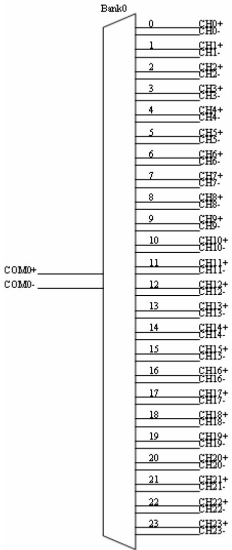
# 2-wire MUX

This configuration has one 24x1 2-wire multiplexer Bank0, which has twentyfour channels. The following diagram illustrates the terminal board pin definition.
![Bank0\n0 CH8+\n1 CH1+\n2 CH2+\n3 CH3+\n4 CH4+\n5 CH5+\n6 CH6+\n7 CH7+\n8 CH8+\n9 CH9+\n10 CH10+\n11 CH11+\n12 CH12+\n13 CH13+\n14 CH14+\n15 CH15+\n16 CH16+\n17 CH17+\n18 CH18+\n19 CH19+\n20 CH20+\n21 CH21+\n22 CH22+\n23 CH23+](.pxi-7921-50-17011-1010-11/a119125c01cc911032da3f2587d4b47fa38df1f27b2e83c4dba3ac77a563b975.jpg)

Figure 3: 24x1 MUX

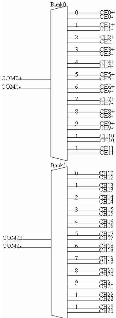
# 2-wire, 2-group MUX

This configuration has two 12x1 2-wire multiplexers Bank0 and Bank1, each has twelve channels. The following diagram illustrates the terminal board pin definition.
![Bank0\nCOM0+\nCOM0-\nBank1\nCOM2+\nCOM2-\n0 CH0+\nCH0-\n1 CH1+\nCH1-\n2 CH2+\nCH2-\n3 CH3+\nCH3-\n4 CH4+\nCH4-\n5 CH5+\nCH5-\n6 CH6+\nCH6-\n7 CH7+\nCH7-\n8 CH8+\nCH8-\n9 CH9+\nCH9-\n1 CH10\n1 CH11\n0 SH12\n1 SH13\n2 SH14\n3 SH15\n4 SH16\n5 SH17\n6 SH18\n7 SH19\n8 SH20\n9 SH21\n1 SH22\n1 SH23](.pxi-7921-50-17011-1010-11/46de1ba9a5415645d5565646db169f78a09d5d0200924c03226dfbe6690b0d79.jpg)

Figure 4: Two 12x1 MUX

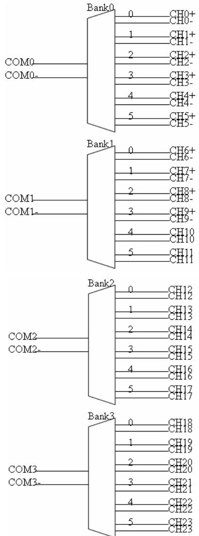
# 2-wire, 4-group MUX

This configuration has four 6x1 2-wire multiplexers Bank0, Bank1, Bank2 and Bank3, each has six channels. The following diagram illustrates the terminal board pin definition.
![The diagram displays four vertical blocks, each representing a switching bank (Bank0 through Bank3). There are no connecting lines between the blocks themselves; instead, each block has independent input connections on the left and output connections on the right.\n\n**Block: Bank0**\n*   **Left Connections:** COM0, COM0-\n*   **Right Connections:**\n    *   0 -) CH0+\n    *   1 -) CH1+\n    *   2 -) CH2+\n    *   3 -) CH3+\n    *   4 -) CH4+\n    *   5 -) CH5+\n\n**Block: Bank1**\n*   **Left Connections:** COM1, COM1-\n*   **Right Connections:**\n    *   0 -) CH6+\n    *   1 -) CH7-\n    *   2 -) CH8+\n    *   3 -) CH9+\n    *   4 -) CH10\n    *   5 -) CH11\n\n**Block: Bank2**\n*   **Left Connections:** COM2, COM2-\n*   **Right Connections:**\n    *   0 -) CH12\n    *   1 -) CH13\n    *   2 -) CH14\n    *   3 -) CH15\n    *   4 -) CH16\n    *   5 -) CH17\n\n**Block: Bank3**\n*   **Left Connections:** COM3, COM3-\n*   **Right Connections:**\n    *   0 -) CH18\n    *   1 -) CH19\n    *   2 -) CH20\n    *   3 -) CH21\n    *   4 -) CH22\n    *   5 -) CH23](.pxi-7921-50-17011-1010-11/0391b11ab27db77b97532c3bfebffcb55508d355089a4b3da332692e1ea56d63.jpg)

Figure 5: Four 6x1 MUX

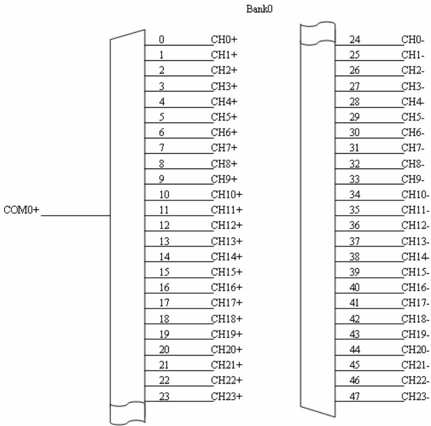
# 1-wire MUX

This configuration has one 48x1 1-wire multiplexer Bank0, which has fortyeight channels. The following diagram illustrates the terminal board pin definition.
![Bank0\nCOM0+\n0 CH0+\n1 CH1+\n2 CH2+\n3 CH3+\n4 CH4+\n5 CH5+\n6 CH6+\n7 CH7+\n8 CH8+\n9 CH9+\n10 CH10+\n11 CH11+\n12 CH12+\n13 CH13+\n14 CH14+\n15 CH15+\n16 CH16+\n17 CH17+\n18 CH18+\n19 CH19+\n20 CH20+\n21 CH21+\n22 CH22+\n23 CH23+\n24 CH0-\n25 CH1-\n26 CH2-\n27 CH3-\n28 CH4-\n29 CH5-\n30 CH6-\n31 CH7-\n32 CH8-\n33 CH9-\n34 CH10-\n35 CH11-\n36 CH12-\n37 CH13-\n38 CH14-\n39 CH15-\n40 CH16-\n41 CH17-\n42 CH18-\n43 CH19-\n44 CH20-\n45 CH21-\n46 CH22-\n47 CH23-](.pxi-7921-50-17011-1010-11/7fb3b830096a352bea0ba2f5f4a0039b4133a3804c75b6a46ad0dc0ef92995b0.jpg)

Figure 6: 48x1 MUX

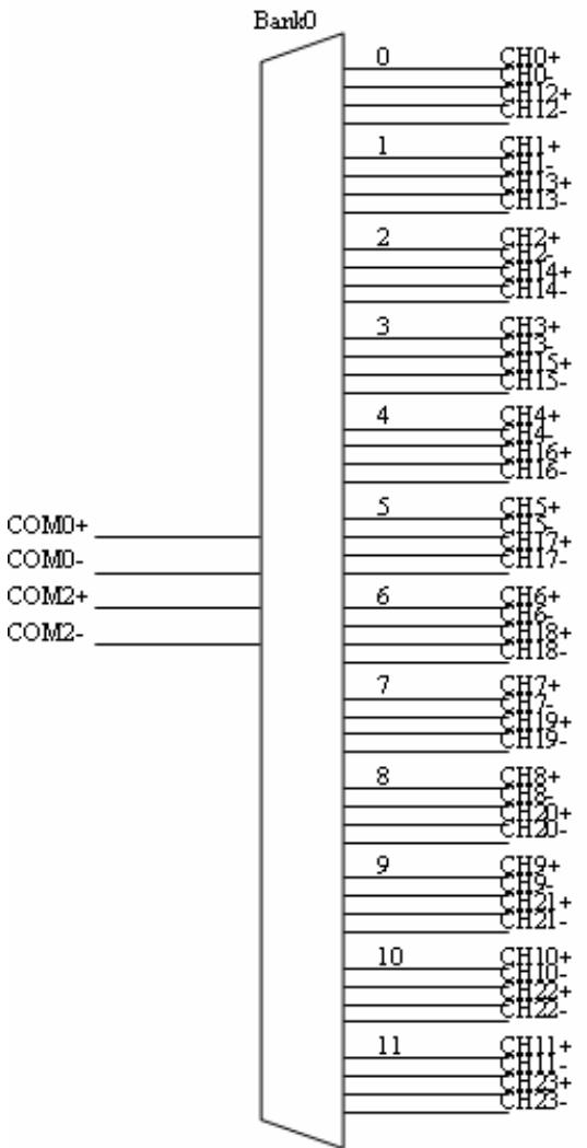
# 4-wire MUX

This configuration has one 12x1 4-wire multiplexer Bank0, which has twelve channels. The following diagram illustrates the terminal board pin definition.
![Bank0\n0 CH0+\nCH12+\nCH12-\n1 CH1+\nCH13+\nCH13-\n2 CH2+\nCH14+\nCH14-\n3 CH3+\nCH15+\nCH15-\n4 CH4+\nCH16+\nCH16-\n5 CH5+\nCH17+\nCH17-\n6 CH6+\nCH18+\nCH18-\n7 CH7+\nCH19+\nCH19-\n8 CH8+\nCH20+\nCH20-\n9 CH9+\nCH21+\nCH21-\n10 CH10+\nCH22+\nCH22-\n11 CH11+\nCH23+\nCH23-](.pxi-7921-50-17011-1010-11/2b2fc25acf3ece93d221ddd19579f6a04c01af1482b85fdcadd02f14d461055c.jpg)

Figure 6: 4-wire MUX

# 4

# Operation Theorem

# 4.1 Hardware Block Diagram

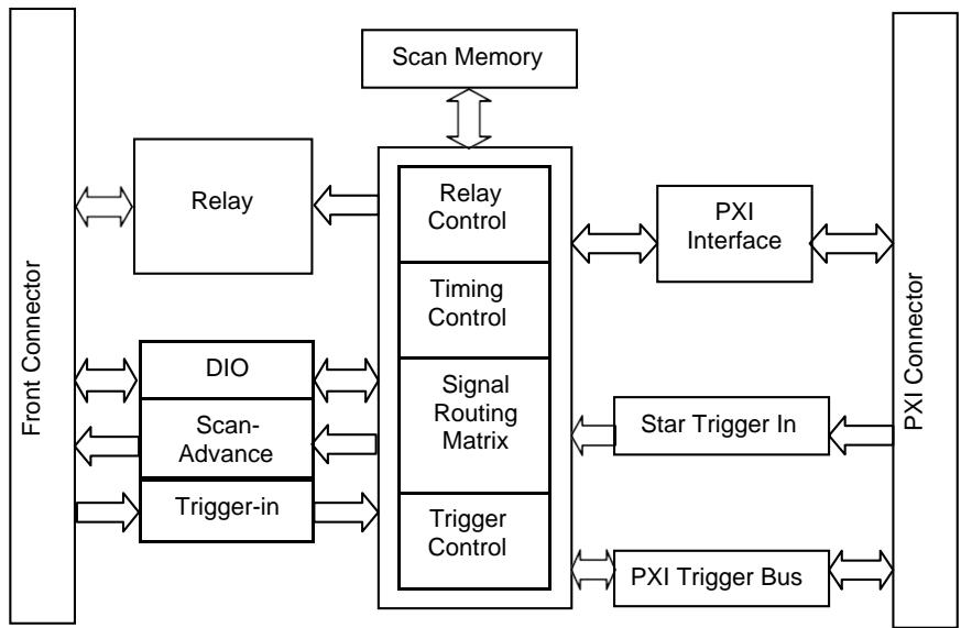
The ADLINK PXI Switch Module features an onboard FPGA for relay switching control, trigger control, scanlist storage and sequencing. The PXI triggering and synchronization functions, such as Star Trigger and Trigger Bus are also supported. In addition to the Trigger In and Scanner Advanced signals for external instruments handshaking, the switch module provides eight channels of programmable digital I/O interface to facilitate general purpose control applications.

To make full use of the flexible trigger and signaling system on the PXI platform, the switch module has a built-in signal routing matrix that can exchange signals between front panel digital I/O, Star Trigger, and Trigger Bus.
![Based on the provided flowchart, here are the labeled blocks and their connections:\n\n**Labeled Blocks:**\n*   **Front Connector** (Vertical bar on the left)\n*   **Relay**\n*   **DIO**\n*   **Scan-Advance**\n*   **Trigger-in**\n*   **Scan Memory** (Top center)\n*   **Central Control Block** (Large rectangle containing four sub-blocks):\n    *   **Relay Control**\n    *   **Timing Control**\n    *   **Signal Routing Matrix**\n    *   **Trigger Control**\n*   **PXI Interface**\n*   **Star Trigger In**\n*   **PXI Trigger Bus**\n*   **PXI Connector** (Vertical bar on the right)\n\n**Connections:**\n*   **Front Connector** connects bidirectionally to **Relay**, **DIO**, and **Scan-Advance**.\n*   **Front Connector** connects unidirectionally (arrow pointing right) to **Trigger-in**.\n*   **Relay** connects bidirectionally to **Relay Control**.\n*   **DIO** connects bidirectionally to the **Central Control Block** (specifically aligned with **Timing Control**).\n*   **Scan-Advance** connects bidirectionally to the **Central Control Block** (specifically aligned with **Signal Routing Matrix**).\n*   **Trigger-in** connects unidirectionally (arrow pointing right) to the **Central Control Block** (specifically aligned with **Trigger Control**).\n*   **Scan Memory** connects bidirectionally to **Relay Control**.\n*   **Relay Control** connects bidirectionally to **PXI Interface**.\n*   **PXI Interface** connects bidirectionally to **PXI Connector**.\n*   **Signal Routing Matrix** connects bidirectionally to **Star Trigger In**.\n*   **Star Trigger In** connects bidirectionally to **PXI Connector**.\n*   **Trigger Control** connects bidirectionally to **PXI Trigger Bus**.\n*   **PXI Trigger Bus** connects bidirectionally to **PXI Connector**.](.pxi-7921-50-17011-1010-11/838bfd3f1ecbc8667a20060e5c8262c997079e7eadc367e131b441be0dc31c4b.jpg)

Figure 7: Hardware Block Diagram

# 4.2 Operation Mode

The ADLINK PXI Switch Module provides two relay operation modes to accommodate different application requirements.

# Direct-update

The Switch Module updates the relay pattern immediately upon receiving a software command. This mode provides a straightforward control over switch module with minimal hardware intervention. If relay contact bouncing is of a concern, users would need to insert software delay.

ADLINK recommends the debounce time to be at least 5ms on PXI-7921.

# Auto-scan

The ADLINK PXI switch module features onboard memory to store user specified scanlist of up to 1024-entry. In each scanlist entry, users can specify relay pattern, pattern advancing delay time and criterion.

The switch module can set status bit or generate local interrupt to inform user’s program whether the pattern has been debounced and advanced to the next scanlist entry. Users can also specify one-time or cyclic scanning of scanlist entries.

This operating mode supports trigger signals for instrument handshaking. For more information on handshaking signals, please refer to section 4.3.

# 4.3 Handshaking

In the Auto-scan mode, ADLINK PXI switch module accepts Trigger In and generates Scanner Advanced signal to synchronize relay switching and measurements with PXI instruments or external measurement devices.

# Trigger In

The Trigger In signal from PXI instruments or external measurement devices instruct the ADLINK PXI switch module to update the relay pattern according to the one specified in the scanlist entry.

Users may specify wait-for-trigger instruction in a scanlist entry, to have the switch module wait for the Trigger In before relay pattern is updated. The polarity of Trigger In can be set to either rising-edge or falling-edge active.

For more information on scanlist configuration, please refer to the software programming users’ guide.

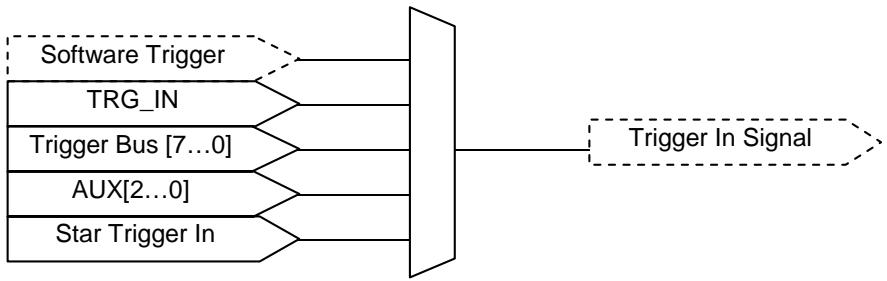
Figure 8 illustrates the available signal sources for the Trigger In signal. Signal names in the solid-line box represent the external (physical) signal on

connectors, and signals in the dotted-line box represents switch module’s internal signal.
![The diagram depicts a logic structure with five input signals feeding into a central block, which produces a single output signal.\n\n**Inputs (Left Side):**\n*   **Software Trigger**: Enclosed in a dashed rectangle. A dashed arrow connects it to the top input of the central block.\n*   **TRG_IN**: Enclosed in a solid rectangle. A solid arrow connects it to the second input of the central block.\n*   **Trigger Bus (7...0)**: Enclosed in a solid rectangle. A solid arrow connects it to the third input of the central block.\n*   **AUX(2...0)**: Enclosed in a solid rectangle. A solid arrow connects it to the fourth input of the central block.\n*   **Star Trigger In**: Enclosed in a solid rectangle. A solid arrow connects it to the bottom input of the central block.\n\n**Central Block:**\n*   A large, vertical trapezoid shape acts as a combiner or logic gate. It receives all five input signals from the left side.\n\n**Output (Right Side):**\n*   A single solid line exits the right side of the central trapezoid.\n*   **Trigger In Signal**: Enclosed in a dashed rectangle. This label represents the output signal generated by the central block.](.pxi-7921-50-17011-1010-11/6d1ee54ab869bd85c25e813ffaa7de90f7f407eb6a87b63f2c4b25005674e810.jpg)

Figure 8: Available signal sources for Trigger In

# Scanner Advanced

After updating the relay pattern, the switch module starts its debounce timer and waits for the relay contacts to settle. When the debounce time elapses, the switch module will generate a Scanner Advanced signal to notify the PXI instruments or external measurement devices that the relay contacts have settled, and ready to take a new measurement.

The waveform, polarity and pulse width of Scanner Advanced signal can also be software programmed.

For more information on scanlist configuration, please refer to the software programming users’ guide.

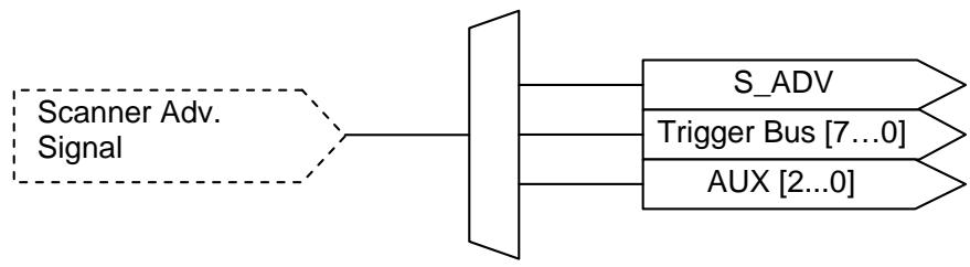
Figure 9 illustrates the available signal destinations for the Scanner Advanced signal. Signal names in the solid-line boxes represent the external (physical) signal on connectors, while signals in the dotted-line boxes represent switch module’s internal signal.
![The diagram displays a signal path starting with a dashed rectangular block on the left containing the text 'Scanner Adv. Signal'. A single horizontal line connects this block to a vertical trapezoidal shape in the center. From the right side of this central shape, three parallel horizontal lines extend to the right, connecting to three arrow-shaped blocks. From top to bottom, these blocks are labeled:\n\n*   **S_ADV**\n*   **Trigger Bus (7...0)**\n*   **AUX (2...0)**](.pxi-7921-50-17011-1010-11/43b1933dc0dc4442d01d0aa8d63a0c9ac53a4e092847dc97b3dd0907aca5642b.jpg)

Figure 9: Available signal destinations for Scanner Advanced

# Handshaking protocol

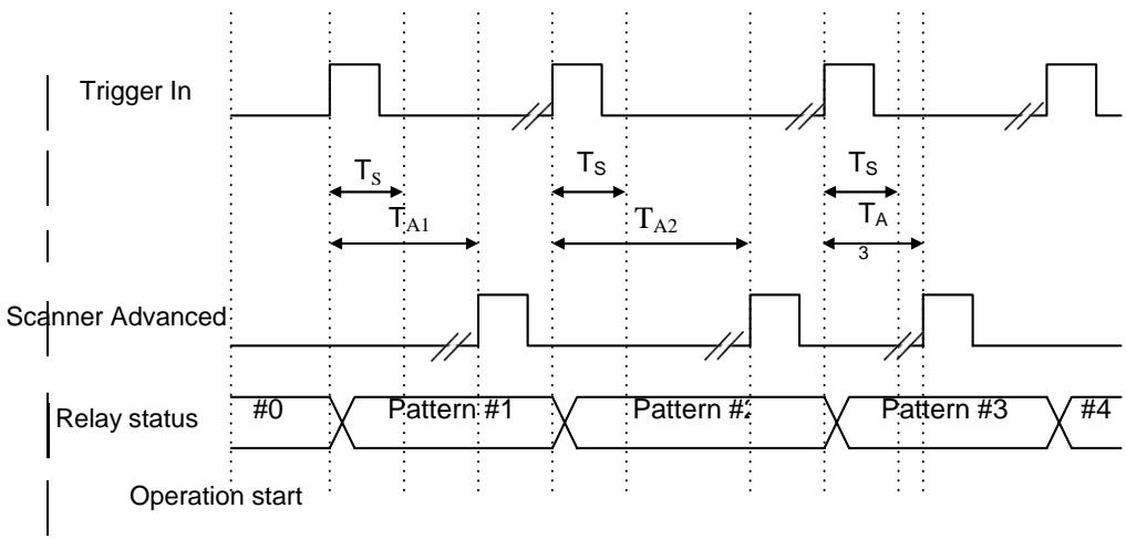
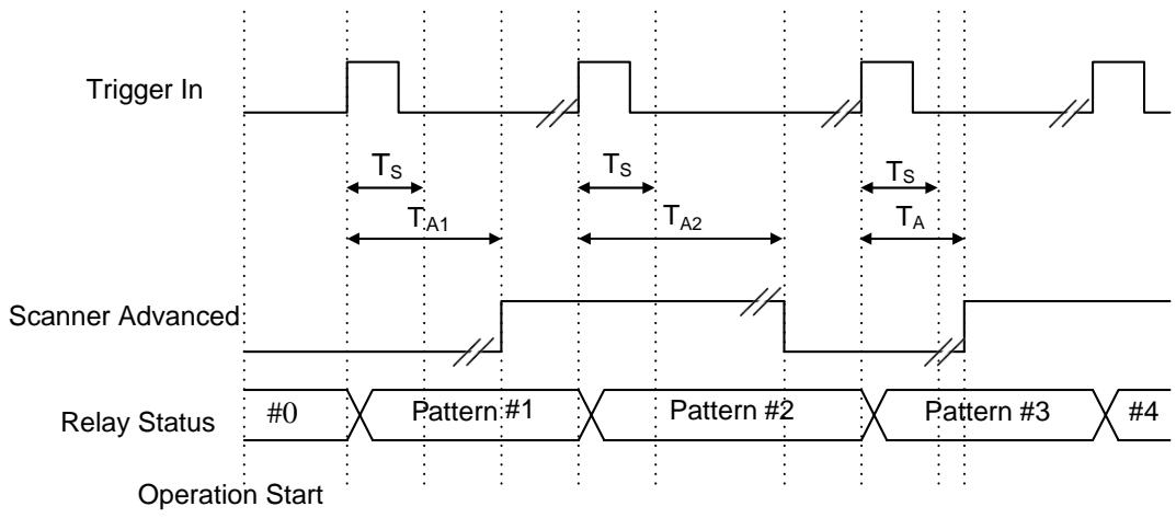
Figures 10 and 11 depict the relationship between Trigger In, Scanner Advanced, and relay pattern in handshaking mode. In Figure 11 the Scanner Advanced is set to pulsating mode.
![Based on the provided image, which is a timing diagram rather than a traditional flowchart, here is the accurate description of the labeled blocks and connections:\n\n**Labeled Blocks and States:**\n*   **Trigger In** (Top signal row)\n*   **Scanner Advanced** (Middle signal row)\n*   **Relay status** (Bottom signal row)\n*   **Operation start** (Bottom left label)\n*   **Time Intervals:** 'Ts', 'TA1', 'TA2', 'TA'\n*   **Index Number:** '3'\n*   **State Labels:** '#0', 'Pattern #1', 'Pattern #2', 'Pattern #3', '#4'\n\n**Connections and Relationships:**\n*   **Signal Synchronization:** Vertical dotted lines connect events across the three rows, indicating synchronization points.\n*   **Sequence:** The 'Relay status' follows a sequential path: it starts at **#0**, transitions to **Pattern #1**, then **Pattern #2**, then **Pattern #3**, and finally moves toward **#4**.\n*   **Timing Relationships:**\n    *   **Ts:** Represents the delay between the rising edge of a 'Trigger In' pulse and the rising edge of a 'Scanner Advanced' pulse.\n    *   **TA1, TA2, TA:** Represent time durations spanning from the start of the trigger pulse to the end of the corresponding 'Scanner Advanced' pulse or pattern cycle.\n    *   The label **3** is positioned below the **TA** interval.\n*   **Triggering:** The 'Scanner Advanced' pulses align with the transitions between the states in 'Relay status' (e.g., the transition from **#0** to **Pattern #1** aligns with the first 'Scanner Advanced' pulse).](.pxi-7921-50-17011-1010-11/142ec3ffcaf82715ed6d750c365c64da0708ebef6936d3386a68f7c55159c951.jpg)

Figure 10: Handshaking operation (Scanner Advanced set in pulsating mode)
![This is a timing diagram illustrating the relationship between three signals over time, aligned by vertical dotted lines.\n\n**Labeled Blocks and Text:**\n*   **Rows:** 'Trigger In', 'Scanner Advanced', 'Relay Status'\n*   **Relay Status Blocks:** '#0', 'Pattern: #1', 'Pattern #2', 'Pattern #3', '#4'\n*   **Annotations:** '\$T_S\$', '\$T_{A1}\$', '\$T_{A2}\$', '\$T_A\$', 'Operation Start'\n\n**Connections and Alignments:**\n*   **Trigger In:** Displays square pulses. '\$T_S\$' indicates pulse width. '\$T_{A1}\$', '\$T_{A2}\$', and '\$T_A\$' indicate time intervals between consecutive pulses. Slashes on the line indicate repeated time intervals.\n*   **Scanner Advanced:** Displays a signal that goes high during the 'Pattern #2' block and low during the 'Pattern #3' block, then goes high again starting at the '#4' block.\n*   **Vertical Alignments:**\n    *   The rising edge of the first 'Trigger In' pulse aligns with the transition from '#0' to 'Pattern: #1'.\n    *   The rising edge of the second 'Trigger In' pulse aligns with the transition from 'Pattern #2' to 'Pattern #3'.\n    *   The rising edge of the third 'Trigger In' pulse aligns with the transition from 'Pattern #3' to '#4'.\n    *   The rising edge of the 'Scanner Advanced' signal aligns with the transition from 'Pattern: #1' to 'Pattern #2'.\n    *   The falling edge of the 'Scanner Advanced' signal aligns with the transition from 'Pattern #2' to 'Pattern #3'.\n    *   The rising edge of the second 'Scanner Advanced' pulse aligns with the transition from 'Pattern #3' to '#4'.](.pxi-7921-50-17011-1010-11/e80b7bd126b3e4ff899970c93bb0b6541ce15e8de73dc32b063fbf03ceaddb3e.jpg)

Figure 11: Handshaking operation (Scanner Advanced set in toggling mode)

Once the operation starts and has received a Trigger In signal, the switch module updates the relay pattern to that specified in the first entry of scanlist.

TS is the default debounce time for a switch module, i.e. 5ms for PXI-7921. TAn is the user specified scan delay time in the scanlist entry, indicating the time between the relay being debounced and the exact moment that a measurement device takes a new measurement. The actual delay time would be the greater of the two times, to guarantee that measurement devices take measurements after the signal path is fully settled, and the relays switch as close as possible to their maximum operating speed.

As the scan delay time elapses, the switch module generates Scanner Advanced signal to inform the measurement device to take a new measurement.

After the measurement completes, the measurement device will generate another Trigger In signal to have the switch module update the relay pattern to that specified in the second entry of scanlist.

The handshaking process will continue, until it reaches the end of the scanlist (if one-time scanning mode is selected), or when a software scan-abort command is received.

# Connecting, Trigger and Synchronize with External DMM

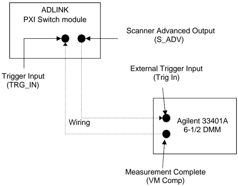
In this example, Agilent® 33401A 6-1/2 Digital Multimeter (DMM) is used to demonstrate signal connection for handshaking operation.

The DMM provides two terminals on the rear panel for the handshaking operation process, Trig In and VM Comp. The Trig In connects to the Scanner Advanced output on switch module, while the VM Comp to Trigger In. If the terminal board is used, wire Trig In to TRG\_IN on terminal board, and the VM Comp to S\_ADV.

Follow the instructions below to ensure the handshake functions properly:

1. Configure ADLINK PXI switch module’s Trigger In to rising-edge triggered, Scanner Advanced output in active-low pulsating mode with pulse width of at least 2us.
2. Configure the DMM to wait for external Trig In before a measurement, and generate VM Comp after a measurement. Arm the DMM to wait for the first trigger.
3. Setup the scanlist and auto-scan mode. The first entry in the scanlist should be set disable wait for the Trigger In, but enable Scanner Advanced output. Succeeding entries should enable both Trigger In and Scanner Advanced output. Download the scanlist to the switch module afterward.
4. Start auto-scan by sending scan start command to the switch module.
![The flowchart depicts a connection diagram between two hardware modules.\n\n**Labeled Blocks:**\n*   **ADLINK PXI Switch module** (top left box)\n*   **Agilent 33401A 6-1/2 DMM** (bottom right box)\n\n**Connections:**\n*   **Scanner Advanced Output (S_ADV)** points to the right black circle inside the **ADLINK PXI Switch module**.\n*   **Trigger Input (TRG_IN)** points to the left black circle inside the **ADLINK PXI Switch module**.\n*   **Wiring** (represented by dotted lines) connects the black circles of the **ADLINK PXI Switch module** to the black circles of the **Agilent 33401A 6-1/2 DMM**. Specifically:\n    *   A dotted line connects the right circle of the **ADLINK PXI Switch module** to the top circle of the **Agilent 33401A 6-1/2 DMM**.\n    *   A dotted line connects the left circle of the **ADLINK PXI Switch module** to the bottom circle of the **Agilent 33401A 6-1/2 DMM**.\n*   **External Trigger Input (Trig In)** points to the top black circle inside the **Agilent 33401A 6-1/2 DMM**.\n*   **Measurement Complete (VM Comp)** points to the bottom black circle inside the **Agilent 33401A 6-1/2 DMM**.](.pxi-7921-50-17011-1010-11/9e3548c0091e4968457dad8e2ec59ead5e3cdb2fc0bd6b291e593fc78f137dc9.jpg)

Figure 12: Signal Connection between Switch Module and Agilent DMM

For more information on scanlist configuration, scan mode setup, start, and stop functions of the auto-scanning process, please refer to the software programming users’ guide.

# 4.4 Trigger Bus

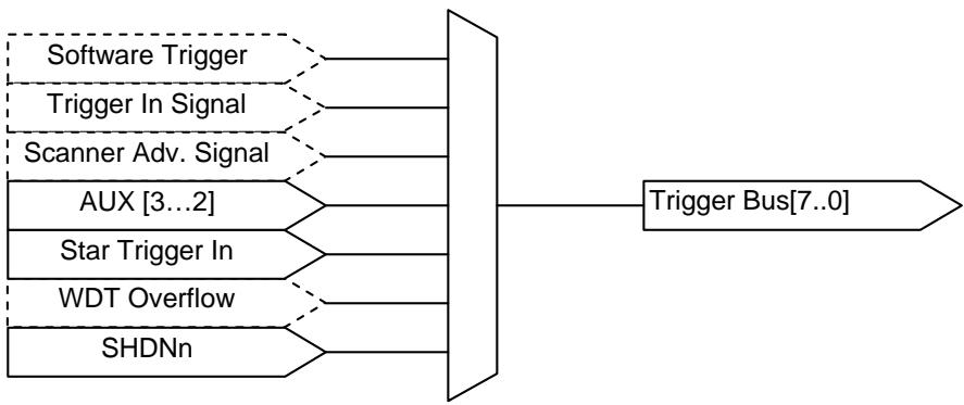
PXI specification defines eight bused-lines across slots in a segment. Users can route various trigger signal to synchronize multiple PXI instruments, and/or simplify field wiring across multiple ADLINK Switch Modules.

On ADLINK Switch Modules, the trigger bus driver is disconnected from PXI trigger bus before users’ configuration.

Figure 13 illustrates the available signal destinations for Trigger Bus[7..0]. Signal names in the solid-line boxes represent the external (physical) signals on connectors while signals in the dotted-line boxes represent the switch module’s internal signal.
![The diagram shows a logic flow with seven input blocks on the left feeding into a central vertical trapezoidal block (likely a multiplexer), which outputs to a single block on the right.\n\n**Labeled Blocks:**\n*   Software Trigger\n*   Trigger In Signal\n*   Scanner Adv. Signal\n*   AUX (3...2)\n*   Star Trigger In\n*   WDT Overflow\n*   SHDNn\n*   Trigger Bus(7..0)\n\n**Connections:**\n*   The blocks 'Software Trigger', 'Trigger In Signal', 'Scanner Adv. Signal', and 'WDT Overflow' connect to the central block via dashed lines.\n*   The blocks 'AUX (3...2)', 'Star Trigger In', and 'SHDNn' connect to the central block via solid lines.\n*   The central block connects to the 'Trigger Bus(7..0)' block via a single solid horizontal line.](.pxi-7921-50-17011-1010-11/52209de2e99eb2fca9a43ed1e4ea48f203c844251e73fe0dd88b2b9d5724e6db.jpg)

Figure 13: Available signal sources for Trigger Bus[7..0]

# 4.5 Auxiliary Digital I/O

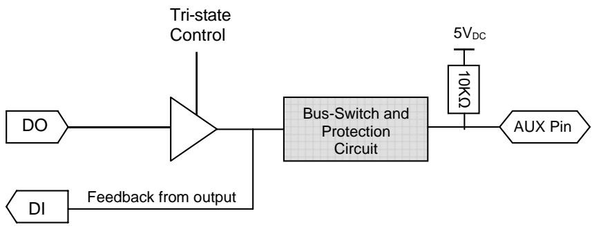
The eight auxiliary digital I/O lines on ADLINK Switch Modules provide versatility to users’ control applications. Each digital I/O line can be input, output or tri-stated. When in output mode, users can still read back the actual logiclevel on the I/O line. All digital lines are pulled-up to 5V with 10k ohm input resistance.

Note that AUX[2..0] are dual function pins, driving these pins while enabling handshaking or emergency shutdown functions, may falsely trigger the Switch Module or external instruments.
![The diagram shows a circuit schematic with the following labeled blocks and connections:\n\n**Blocks and Labels:**\n*   **DO**\n*   **DI**\n*   **Tri-state Control**\n*   **Feedback from output**\n*   **Bus-Switch and Protection Circuit**\n*   **5VDC**\n*   **10kΩ**\n*   **AUX Pin**\n\n**Connections:**\n1.  **DO** connects to the input of a triangular buffer.\n2.  **Tri-state Control** connects to the top input of the triangular buffer.\n3.  The output of the triangular buffer splits into two paths:\n    *   One path connects to the input of the **Bus-Switch and Protection Circuit**.\n    *   The other path connects to **DI** via a wire labeled **Feedback from output**.\n4.  The output of the **Bus-Switch and Protection Circuit** connects to **AUX Pin**.\n5.  A resistor labeled **10kΩ** connects the line between the **Bus-Switch and Protection Circuit** and **AUX Pin** to **5VDC**.](.pxi-7921-50-17011-1010-11/b933a9bed5765a0af9feceaf6efe53a2fba4f79d2c571d23fe8627e773ba523d.jpg)

Figure 11: Auxiliary Digital I/O Function Block

# 4.6 Hot-Swap

The Switch Module can be hot-swapped during hardware failure in noninterruptible or high-availability systems where system shutdown is not an option.

PXI-7921 incorporates an onboard hot-swap control mechanism. However the extent of the hot-swap functionality support depends on the operating system and the PXI platform.

Microsoft Embedded $\mathsf { X P } ^ { \circledast }$ supports the native hot-swap function. The operating system automatically releases system resources when a switch module is extracted and recognizes the new device.

To remove a switch module, first release the screws on the front panel then push down the red latch on the ejector. When the blue LED turns on, the Switch module is ready to be removed by fully pushing down the ejector.

To insert another switch module, align the module’s edge with the card guide in the PXI chassis. Slide the switch module into the chassis, until there is resistance from the PXI connector. Push the ejector up and fully insert the switch module into the chassis, a click should be heard from the ejector latch. The blue LED on the front panel of the switch module will switch off when it is ready for operation. Tighten the screws on the front panel.

Note: Microsoft Windows $2 0 0 0 ^ { \circledast }$ does not natively support hot-swap however, PXI-7921 can be hot-swapped by manual control via an additional hot-swap driver. For the hot-swap driver on Windows 2000 and other operating systems such as Linux, VxWorks, etc., please contact ADLINK for more information.

# 4.7 Emergency Shutdown

In safety-critical applications, users can enable the emergency shutdown function on PXI Switch Module, to manually set the relay pattern to preset state.

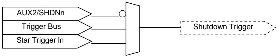
To access this function, users must first configure the emergency shutdown function by windows API. Generally the trigger source is on the front panel and connected to a push button, which pulls the SHDNn pin to logic-low when activated. When multiple PXI Switch modules are installed in a PXI chassis, the trigger source can be routed through the PXI Trigger Bus and eliminate field wiring across multiple devices. Figure 12 illustrates available trigger sources for emergency shutdown. Signal names in the solid-line boxes represent the external (physical) signal on connectors and signals in the dotted-line boxes represent the switch module’s internal signal.
![The diagram displays three input lines on the left labeled 'AUX2/SHDNn', 'Trigger Bus', and 'Star Trigger In'. These lines feed into a central vertical block. The connection for 'AUX2/SHDNn' features a small circle near the block. A single line exits the right side of the central block and connects to a dashed rectangular block containing the text 'Shutdown Trigger'.](.pxi-7921-50-17011-1010-11/1a8be6dbedbe8d66906f113f4b61b62f8328db03ed2b392567af23308282eb92.jpg)

Figure 12: Available trigger sources for emergency shutdown

The default relay pattern for emergency shutdown is All-Off on PXI-7921; users can change the pattern by Windows API.

Upon receiving the emergency shutdown trigger, the Switch Module enters shutdown mode, and the relay pattern is switched to the preset state. If the Switch Module is in Auto-scan mode, the updating process would be stopped immediately; in Direct Update mode where the switch module will not accept any further update instructions.

To leave emergency shutdown mode, users must call adlSwitch\_Recovery in Windows API. The relay pattern would stay the same as they would in the emergency shutdown mode, and the scanlist (if set) being rewound to the first entry.

Note the auxiliary digital I/O function pin AUX2 shares the SHDNn pin; driving AUX2 to logic-low while the emergency shutdown function is enabled. It will falsely trigger the Switch Module to enter shutdown mode.

This function is disabled by default. For more information, please refer to the software programming users’ guide.

# 4.8 Watchdog Timer

In safety-critical applications, users can enable the watchdog timer function on PXI Switch Module to automatically set the relay pattern to preset state, in case the operating system or PXI controller crashes.

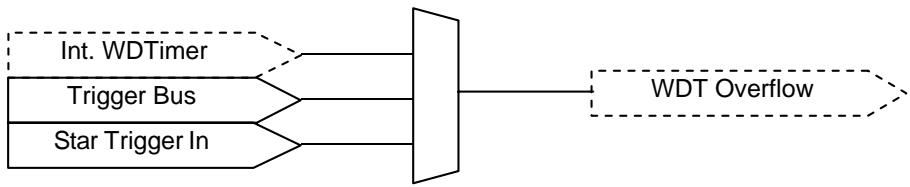
To access this function, users must first configure the watchdog timer overflow trigger source by windows API. Generally the trigger source would come from the onboard 32-bit watchdog timer. When multiple ADLINK PXI Switch modules are installed in a PXI chassis, the trigger source can be routed through the PXI Trigger Bus and eliminate redundant watchdog timer setting on multiple devices.

Figure 13 illustrates the available trigger sources for watchdog timer overflow. Signal names in the solid-line boxes represent the external (physical) signal on connectors and signals in the dotted-line boxes represent the switch module’s internal signal.
![This flowchart depicts a signal routing mechanism with three inputs converging into a single output.\n\n**Labeled Blocks:**\n*   **Int. WDTimer** (top left, enclosed in a dashed border)\n*   **Trigger Bus** (middle left, enclosed in a solid border)\n*   **Star Trigger In** (bottom left, enclosed in a solid border)\n*   **WDT Overflow** (far right, enclosed in a dashed border)\n*   **Central Component** (unlabeled vertical trapezoid in the middle)\n\n**Connections:**\n*   Lines originate from **Int. WDTimer**, **Trigger Bus**, and **Star Trigger In** and converge into the left side of the central trapezoidal component.\n*   A single line exits the right side of the central trapezoidal component and connects to **WDT Overflow**.](.pxi-7921-50-17011-1010-11/942036bd33b2f5ec756192f4b1a8b43695108d81b3b8dc78cea7c72f8ee9dad8.jpg)

Figure 13:.Available trigger sources for watchdog timer overflow

The watchdog timer overflow interval can be programmed through Windows API. After enabling the watchdog timer, users must periodically reset the timer by software command. If the timer is not being reset within the specified interval, the switch module will generate an overflow signal and set the relay pattern to the one specified by users.

This function is disabled by default. For more information, please refer to the software programming users’ guide.

# Warranty Policy

Thank you for choosing ADLINK. To understand your rights and enjoy all the after-sales services we offer, please read the following carefully:

1. Before using ADLINK’s products please read the user manual and follow the instructions exactly.
2. When sending in damaged products for repair, please attach an RMA application form.
3. All ADLINK products come with a two-year guarantee, repaired free of charge.

The warranty period starts from the product’s shipment date from ADLINK’s factory.
Peripherals and third-party products not manufactured by ADLINK will be covered by the original manufacturers’ warranty.
End users requiring maintenance services should contact their local dealers. Local warranty conditions will depend on local dealers.

4. This warranty will not cover repair costs due to:

a. Damage caused by not following instructions.
b. Damage caused by carelessness on the users’ part during product transportation.
c. Damage caused by fire, earthquakes, floods, lightening, pollution, other acts of God, and/or incorrect usage of voltage transformers.
d. Damage caused by unsuitable storage environments (i.e. high temperatures, high humidity, or volatile chemicals.
e. Damage caused by leakage of battery fluid.
f. Damage from improper repair by unauthorized technicians.
g. Products with altered and/or damaged serial numbers.
h. Other categories not protected under our guarantees.

5. Customers are responsible for shipping costs to transport damaged products to our company or sales office.

6. To ensure the speed and quality of product repair, please download a RMA application form from our company website: www.adlinktech.com. Damaged products with attached RMA forms receive priority.

For further questions, please contact our FAE staff.

ADLINK: service@adlinktech.com
[🔗 Link to the original document](.pxi-7921-50-17011-1010-11/pxi-7921-50-17011-1010-11.pdf)
