# PCI/PXI-9816/26/46

4-CH 16-Bit 10/20/40 MS/s Digitizer

with 512 MB SDRAM

User’s Manual

Manual Rev. 2.02

Revision Date: October 5, 2010

Part No: 50-17031-1020

![The image displays the universal recycling symbol. It features three white arrows arranged in a clockwise, triangular formation against a solid black circular background. There is no text present in the image.](.pxi-98x6-50-17031-1020-001/cc6308b958ee67a31723ba40eebbba7c8e8ee9bb5f0d36351a89548807d77218.jpg)
Recycled Paper

Copyright 2010 ADLINK TECHNOLOGY INC.

All Rights Reserved.

The information in this document is subject to change without prior notice in order to improve reliability, design, and function and does not represent a commitment on the part of the manufacturer.

In no event will the manufacturer be liable for direct, indirect, special, incidental, or consequential damages arising out of the use or inability to use the product or documentation, even if advised of the possibility of such damages.

This document contains proprietary information protected by copyright. All rights are reserved. No part of this manual may be reproduced by any mechanical, electronic, or other means in any form without prior written permission of the manufacturer.

# Trademarks

NuDAQ, NuIPC, DAQBench are registered trademarks of ADLINK TECHNOLOGY INC.

Product names mentioned herein are used for identification purposes only and may be trademarks and/or registered trademarks of their respective companies.

# Getting Service from ADLINK

Contact us should you require any service or assistance.

# ADLINK Technology, Inc.

Address: 9F, No.166 Jian Yi Road, Chungho City, Taipei County 235, Taiwan ؀קᗼխࡉؑ৬ԫሁ 166 ᇆ 9 ᑔ

Tel: +886-2-8226-5877

Fax: +886-2-8226-5717

Email: service@adlinktech.com

# Ampro ADLINK Technology, Inc.

Address: 5215 Hellyer Avenue, #110, San Jose, CA 95138, USA

Tel: +1-408-360-0200

Toll Free: +1-800-966-5200 (USA only)

Fax: +1-408-360-0222

Email: info@adlinktech.com

# ADLINK Technology (China) Co., Ltd.

Address: Ϟ⍋Ꮦ⌺ϰᮄऎᓴ∳催⾥ᡔುऎ㢇᯹䏃 300 ো(201203) 300 Fang Chun Rd., Zhangjiang Hi-Tech Park, Pudong New Area, Shanghai, 201203 China

Tel: +86-21-5132-8988

Fax: +86-21-5132-3588

Email: market@adlinktech.com

# ADLINK Technology Beijing

Address: ࣫ҀᏖ⍋⎔ऎϞഄϰ䏃 1 োⲜ߯ ࡯ࡼ ໻ॺ E ᑻ 801 ᅸ(100085) Rm. 801, Power Creative E, No. 1, B/D Shang Di East Rd., Beijing, 100085 China

Tel: +86-10-5885-8666

Fax: +86-10-5885-8625

Email: market@adlinktech.com

# ADLINK Technology Shenzhen

Address: ⏅ഇᏖफቅऎ⾥ᡔುफऎ催ᮄफϗ䘧᭄ᄫᡔᴃು A1 ᷟ 2 ὐ C ऎ (518057) 2F, C Block, Bldg. A1, Cyber-Tech Zone, Gao Xin Ave. Sec. 7, High-Tech Industrial Park S., Shenzhen, 518054 China

Tel: +86-755-2643-4858

Fax: +86-755-2664-6353

Email: market@adlinktech.com

# ADLINK Technology (Europe) GmbH

Address: Nord Carree 3, 40477 Duesseldorf, Germany

Tel: +49-211-495-5552

Fax: +49-211-495-5557

Email: emea@adlinktech.com

# ADLINK Technology, Inc. (French Liaison Office)

Address: 15 rue Emile Baudot, 91300 Massy CEDEX, France

Tel: +33 (0) 1 60 12 35 66

Fax: +33 (0) 1 60 12 35 66

Email: france@adlinktech.com

# ADLINK Technology Japan Corporation

	

Address: 151-0072

1-1-2  8F

Asahiseimei Hatagaya Bldg. 8F

1-1-2 Hatagaya, Shibuya-ku, Tokyo 151-0072, Japan

Tel: +81-3-4455-3722

Fax: +81-3-5333-6040

Email: japan@adlinktech.com

# ADLINK Technology, Inc. (Korean Liaison Office)

Address: 昢殾柢 昢爎割 昢爎壟 1506-25 穢壊 B/D 2 猻

2F, Hando B/D, 1506-25, Seocho-Dong, Seocho-Gu, Seoul 137-070, Korea

Tel: +82-2-2057-0565

Fax: +82-2-2057-0563

Email: korea@adlinktech.com

# ADLINK Technology Singapore Pte. Ltd.

Address: 84 Genting Lane #07-02A, Cityneon Design Centre, Singapore 349584

Tel: +65-6844-2261

Fax: +65-6844-2263

Email: singapore@adlinktech.com

# ADLINK Technology Singapore Pte. Ltd. (Indian Liaison Office)

Address: No. 1357, "Anupama", Sri Aurobindo Marg, 9th Cross, JP Nagar Phase I, Bangalore - 560078, India

Tel: +91-80-65605817

Fax: +91-80-22443548

Email: india@adlinktech.com

# Table of Contents

# Table of Contents..........

# List of Tables ......... iii

# List of Figures ......... iv

# 1 Introduction .......

1.1 Features... 3
1.2 Applications .. 3
1.3 Specifications.... 4

# 2 Getting Started ....... 1 9

2.1 Installation Environment . 1 9
2.2 Package Contents . 20
2.3 Mechanical Drawing and I/O Connectors . 21
2.4 Installing the module... 23
2.5 Software Support .. 24

Driver Support for Windows .. 24

WD-DASK (Legacy Drivers and Support) . 26

# 3 Operation Theory ........ 27

3.1 Functional Block Diagram.. 27
3.2 Basic AI Acquisition ... 28

Analog Input Path
Basic Acquisition Timing . 28
AI Data Format . 30

3.3 ADC Sampling Rate and TIMEBASE Control... . 31

Internal Oscillator . 31
External Clock Through Front Panel . . 31
External Clock from PXI Interfaces . 32
Sampling Rate Control . . 32
Timebase Exporting . 33

3.4 Trigger Sources .. 34

Software Trigger . 34
External Digital Trigger . 35
Analog Trigger .. 36
PXI STAR Trigger .. 37
PXI Trigger Bus . 37

Trigger Signal Exporting ... 38

3.5 Trigger Modes... 39

Post-trigger Acquisition . 39

Pre-trigger Acquisition .. 40

Middle-trigger Acquisition .. 41

Delay-trigger Acquisition .. 41

Post-trigger or Delay-trigger Acquisition with Re-trigger . 42

3.6 Data Transfers .. 43

3.7 Synchronizing Multiple Modules .. 44

SSI\_TIMEBASE .. 47

SSI\_TRIG1 .. 48

SSI\_TRIG2 and SSI\_START\_OP .. 49

Comparing the Different Trigger Sources from SSI ...... 50

3.8 Physical Location of the PXI and PCI Digitizer ....... 5 2

Identify PXI Digitizer’s Physical Location by Geographic Address . . 52

Assign a Board ID to a PCI Digitizer . 52

# Important Safety Instructions....... .... 55

# List of Tables

Table 1-1: Analog Input Specifications 4

Table 1-2: Offset and Gain Error 4

Table 1-3: -3dB Bandwidth, typical 5

Table 1-4: System Noise 7

Table 1-5: Spectral Characteristics – PCI/PXI-9816 8
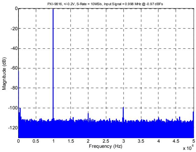
Table 1-6: Spectral Characteristics – PXI-9826 ... 10

Table 1-7: Spectral Characteristics – PCI/PXI-9846 ......... 12

Table 1-8: Timebase 1 4

Table 1-9: Triggering 1 5

Table 1-10: Data Storage and Transfer 1 6

Table 1-11: Onboard Reference . 1 6

Table 1-12: General Information 17

Table 2-1: Connector Pin Assignments . 22

Table 3-1: Basic Counters 29

Table 3-2: AI Data Format 30

Table 3-3: Ideal Transfer Characteristics for Analog Triggers . 36

Table 3-4: Summary of SSI timing Signals and the Corresponding Function 44

Table 3-5: SSI Signal Locations and Pin Definition ........... . 47

Table 3-6: Board ID Combination Conditions 54

# List of Figures

Figure 1-1: PCI/PXI-9816 Bandwidth Chart (50 Ω input impedance) .. 6

Figure 1-2: PCI/PXI-9826 Bandwidth Chart (50 Ω input impedance) . 6

Figure 1-3: PXI-9846 Bandwidth Chart (50 Ω input impedance).. 7

Figure 1-4: PXI-9816 FFT with ±0.2 V Input Range..... 8

Figure 1-5: PXI-9816 FFT with ±1 V Input Range.... 9

Figure 1-6: PXI-9826 FFT with ±0.2 V Input Range...... 1 0

Figure 1-7: PXI-9826 FFT with ±1 V Input Range.. 11

Figure 1-8: PXI-9846 FFT with ±0.2 V Input Range..... 1 2

Figure 1-9: PXI-9846 FFT with ±1 V Input Range.... 1 3

Figure 2-1: PXI-98x6 Mechanical Drawing..... 21

Figure 2-2: PCI-98x6 Mechanical Drawing .... 21

Figure 2-3: DAQPilot Main Interface .. 2 4

Figure 2-4: DAQMaster Device Manager.... 2 5

Figure 2-5: Legacy Software Support Overview . 26

Figure 3-1: PXI-98x6 Functional Block Diagram 2 7

Figure 3-2: PCI-98x6 Functional Block Diagram... 27

Figure 3-3: Analog Input Signal Block Diagram . 28

Figure 3-4: Basic Acquisition Timing Of Digitizer ... 30

Figure 3-5: PCI/PXI-98x6 Timebase Source and Architecture... 31

Figure 3-6: Configuring Different Sampling Rate of a Digitizer. . 33

Figure 3-7: PCI/PXI-98x6 Trigger Architecture .. . 34

Figure 3-8: External Digital Trigger Polarity and Pulse Width Requirement. 35

Figure 3-9: Analog Trigger Conditions . 3 7

Figure 3-10: TRG IO Output Signal Timing...... 3 8

Figure 3-11: Post-trigger Acquisition.. 39

Figure 3-12: Pre-trigger Mode Operation.. 40

Figure 3-13: Pre-trigger Mode Operation.. 40

Figure 3-14: Middle-trigger Mode Operation... 41

Figure 3-15: Delay-trigger Mode Operation .. 4 1

Figure 3-16: Re-trigger Mode Operation... 4 2

Figure 3-17: Scatter-Gather DMA for Data Transfer.... 43

Figure 3-18: SSI Architecture.. 45

Figure 3-19: SSI Connector Location on the PCI-9816/26/46...... 46

Figure 3-20: Installation of ACL-SSI-2 Cable... 4 6

Figure 3-21: SSI\_TRIG1 Input and Output Timing

Characteristics... 48

Figure 3-22: SSI\_TRIG2 Output Timing.. 4 9

Figure 3-23: SSI\_TRIG2 Input Timing Requirement.... 4 9

Figure 3-24: SSI\_START\_OP Output and Input Timing Characteristics.. 50

Figure 3-25: The Location of Board ID Switch . 5 3

Figure 3-26: Enlargement of Board ID setting. .. 53

# 1 Introduction

The ADLINK PCI/PXI-9816/26/46 are 10 MS/s, 20 MS/s, and 40 MS/s sampling 16-bit 4-CH digitizers designed for digitizing high frequency and wide dynamic range signals with an input frequency up to 20 MHz. The analog input range can be programmed via software to ±1 V or ±0.2 V. With deep onboard acquisition memory up to 512 MB, the PCI/PXI-9816/26/46 are not limited by the data transfer rate of the PCI bus to enable the recording of waveforms for extended periods of time.

The PCI/PXI-9816/26/46 are equipped with four high linearity 16- bit A/D converters ideal for demanding applications with a high dynamic range such as radar, ultrasound, and software-defined radio.

# Analog Input

The PCI/PXI-9816/26/46 each feature four analog input channels. The bandwidth of each channel can be up to 5 MHz, 10 MHz, and 20 MHz for PCI/PXI-9816, PCI/PXI-9826, and PCI/PXI-9846, respectively. The input ranges are software programmable as either ±1 V or ±0.2 V. Software selectable 50 Ω input impedance makes it easy to interface with high-speed, high-frequency signals.

# Acquisition System and On-board Memory

The PCI/PXI-9816/26/46 include four 16-bit A/D converters to digitize the input signals. These four channels sample signals simultaneously at a maximum sampling rate of 10 MS/s, 20 MS/s, and 40 MS/s, respectively. The PCI/PXI-9816/26/46 supports a total of 512 MB on-board memory. The digitized data is stored in the onboard memory before being transferred to the host memory. The data transfer is performed using scatter-gather DMA, which provides a high data throughput rate and uses system memory more effectively.

# Flexible Triggering

The PCI/PXI-9816/26/46 feature flexible triggering options such as a software trigger, external digital trigger, an analog trigger from any of the analog input channels and triggers from the PXI trigger bus. These versatile trigger sources allow you to configure the PCI/PXI-9816/26/46 to fit your application needs. Post-trigger, delay-trigger, pre-trigger and middle-trigger modes are also available to acquire data around the trigger event. The PCI/PXI-9816/ 26/46 also features repeated trigger acquisition, so you can acquire data in multiple segments with successive trigger events at extremely short rearming intervals.

# Multiple-Module Synchronization

The versatile trigger options provided by the PXI backplane allow the PCI/PXI-9816/26/46 to achieve multi-module synchronization in a simplified way. Utilizing the PXI Trigger bus, the PCI/PXI-9816/26/46 can output trigger signals and the timebase to the PXI trigger bus when configured as a master, or receive trigger signals and the timebase from the PXI trigger bus when configured as a slave. Moreover, when the PCI/PXI-9816/26/46 is plugged into a peripheral slot of a PXI system, they can also receive triggers or the timebase from the PXI star trigger controller slot. The precision 10 MHz clock that comes from the PXI backplane can also be used as one of the timebase sources. Combining these PXI trigger features with the interface of the PCI/PXI-9816/26/46 makes it very easy to synchronize multiple modules.

# Calibration

The PCI/PXI-9816/26/46 include a precision on-board reference with very low temperature drift. This feature not only provides a stable calibration source for auto-calibration but also maintains stable acquisition accuracy over a wide temperature range. The automated calibration process can be done through software without need for any manually adjustments. Once the calibration process has completed, the calibration information will be stored in the on-board EEPROM so that the values can be loaded and used as needed by the board.

# 1.1 Features

 3U Eurocard form factor (PXI version)
 Standard height, half-length PCI form factor (PCI version)
 Support 5 V and 3.3 V PCI signaling
 Support 32-bit / 66 MHz PCI interface
 4 channels simultaneous single-ended analog input
 16-bit high resolution ADC
 Up to 10 MS/s, 20 MS/s and 40 MS/s per channel
 512 MB onboard memory for data storage
 Software selectable 50 Ω or 1 MΩ input impedance
 Programmable input voltage range: ±0.2V/±1V or ±1V/±5V
 5 MHz, 10 MHz and 20 MHz analog input bandwidth for PCI/PXI-9816, PCI/PXI-9826 and PCI/PXI-9846, respectively
 Multiple modules synchronization through PXI trigger bus
 Support scatter gather DMA transfer
 Fully auto calibration
 90 dBc SFDR, 79 dBc SINAD and 12.8-bit ENOB (PXI-9816)

# 1.2 Applications

 Software radio/wireless communication
 Radar/Sonar/Lidar
 Ultrasound
 Imaging
 Military/Laboratory/Research

# 1.3 Specifications

# Analog Input

<table><tr><td>Specification</td><td>Value</td></tr><tr><td>Number of Channels</td><td>4 single-ended channels</td></tr><tr><td>Input Connector</td><td>BNC</td></tr><tr><td>Input Impedance</td><td>50 Ω or 1 MΩ, software selectable, default 50Ω</td></tr><tr><td>Input Coupling</td><td>DC</td></tr><tr><td>Input Range</td><td>(±0.2V, ±1V) or (±1V, ±5V), software selectable</td></tr><tr><td>Overvoltage Protection</td><td>±5V for (±0.2V, ±1V)±15V for (±1V, ±5V)</td></tr><tr><td>ADC Resolution</td><td>16-Bit, 1 in 65536</td></tr><tr><td>Crosstalk</td><td>≤-80 dB at 1MHz, for all input ranges at 50 Ω input impedance</td></tr></table>

Table 1-1: Analog Input Specifications

<table><tr><td colspan="5">Offset Error</td></tr><tr><td>Model Name</td><td colspan="2">PXI-9816DPXI-9826DPXI-9846DPXI-9846WPCI-9846D</td><td colspan="2">PXI-9846H,PCI-9816HPCI-9826HPCI-9846H</td></tr><tr><td>Offset Error</td><td colspan="2">±0.2 mV</td><td colspan="2">±0.3 mV</td></tr><tr><td colspan="5">Gain Error</td></tr><tr><td>Input Range</td><td>±0.2 V</td><td>±1 V</td><td>±1 V</td><td>±5 V</td></tr><tr><td>Gain Error</td><td>±0.1%</td><td>±0.05%</td><td>±0.1%</td><td>±0.06%</td></tr><tr><td colspan="5">Note: When calculating offset error and gain error, sampled data are averaged with 65536 points and AI channel configured with 50 Ω input impedance.</td></tr></table>

Table 1-2: Offset and Gain Error

<table><tr><td colspan="5">-3dB Bandwidth, typical</td></tr><tr><td>Input Range</td><td>PXI-9816D</td><td>PXI -9826D</td><td>PXI-9846DPCI-9846D</td><td>PXI-9846W</td></tr><tr><td colspan="5">@50 Ω and 1 MΩ impedance</td></tr><tr><td>±0.2 V, ±1 V</td><td>5.1 MHz</td><td>9.6 MHz</td><td>20 MHz</td><td>80 MHz (±1 V)50 MHz (±0.2 V)</td></tr><tr><td>Input Range</td><td>PCI-9816H</td><td>PCI-9826H</td><td>PXI-9846HPCI-9846H</td><td>---</td></tr><tr><td colspan="5">@50 Ω and impedance</td></tr><tr><td>±1 V, ±5 V</td><td>5.1 MHz</td><td>9.6 MHz</td><td>20 MHz</td><td>---</td></tr><tr><td colspan="5">@ 1 MΩ impedance</td></tr><tr><td>±1 V, ±5 V</td><td colspan="3">90 KHz</td><td>---</td></tr></table>

Table 1-3: -3dB Bandwidth, typical

![| Frequency (Hz) | Amplitude (dB) |\n| -------------- | -------------- |\n| 0.1M           | 0              |\n| 1M             | -0.5           |\n| 10M            | -10            |](.pxi-98x6-50-17031-1020-001/93bd86dbaeaff1e89e2698ac4c2b31e882541a9ea617e00e709f875a307c48d1.jpg)

Figure 1-1: PCI/PXI-9816 Bandwidth Chart (50 Ω input impedance)

![| Frequency (Hz) | Amplitude (dB) |\n| -------------- | -------------- |\n| 0.1M           | 0              |\n| 1M             | -0.5           |\n| 10M            | -3.0           |\n| )10M           | -10            |](.pxi-98x6-50-17031-1020-001/28c0d44b57ccb4a60108829a41669a575c5810e149ce70b435d5d2636135c02e.jpg)

Figure 1-2: PCI/PXI-9826 Bandwidth Chart (50 Ω input impedance)

![| Frequency (Hz) | Amplitude (dB) |\n| -------------- | -------------- |\n| 0.1M           | 0              |\n| 1M             | 0              |\n| 10M            | -2             |\n| )10M           | -10            |](.pxi-98x6-50-17031-1020-001/6a9e6e322d3c8db6b1042530f5286ae504f319f73700ed713bf6eaa3d65f3129.jpg)

Figure 1-3: PXI-9846 Bandwidth Chart (50 Ω input impedance)

<table><tr><td colspan="6">System Noise (measured and calculated under 50 Ω input impedance)</td></tr><tr><td>Input Range</td><td>PXI-9816D</td><td>PXI-9826D</td><td>PXI-9846D</td><td>PXI-9846W</td><td>PCI-9846D</td></tr><tr><td>±0.2 V</td><td> $5.0 \text{LSB}_{\text{RMS}}$ </td><td> $6.0 \text{LSB}_{\text{RMS}}$ </td><td> $8.0 \text{LSB}_{\text{RMS}}$ </td><td> $15.0 \text{LSB}_{\text{RMS}}$ </td><td> $8.0 \text{LSB}_{\text{RMS}}$ </td></tr><tr><td>±1 V</td><td> $3.0 \text{LSB}_{\text{RMS}}$ </td><td> $4.0 \text{LSB}_{\text{RMS}}$ </td><td> $5.0 \text{LSB}_{\text{RMS}}$ </td><td> $7.0 \text{LSB}_{\text{RMS}}$ </td><td> $5.0 \text{LSB}_{\text{RMS}}$ </td></tr><tr><td>Input Range</td><td>PCI-9816H</td><td>PCI-9826H</td><td>PCI-9846H</td><td>PXI-9846H</td><td></td></tr><tr><td>±1 V</td><td> $5.0 \text{LSB}_{\text{RMS}}$ </td><td> $6.0 \text{LSB}_{\text{RMS}}$ </td><td> $8.0 \text{LSB}_{\text{RMS}}$ </td><td> $8.0 \text{LSB}_{\text{RMS}}$ </td><td></td></tr><tr><td>±5 V</td><td> $3.0 \text{LSB}_{\text{RMS}}$ </td><td> $4.0 \text{LSB}_{\text{RMS}}$ </td><td> $5.0 \text{LSB}_{\text{RMS}}$ </td><td> $5.0 \text{LSB}_{\text{RMS}}$ </td><td></td></tr></table>

Table 1-4: System Noise

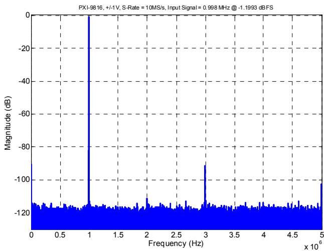
Spectral Characteristics – PXI-9816

<table><tr><td rowspan="2">Specification</td><td colspan="2">Input Range</td></tr><tr><td>±1 V</td><td>±0.2 V</td></tr><tr><td>Signal to Noise and Distortion (SINAD), typical</td><td>79.11 dBc</td><td>75.93 dBc</td></tr><tr><td>Signal-to-Noise Ratio (SNR), typical</td><td>79.36 dBc</td><td>75.96 dBc</td></tr><tr><td>Total Harmonic Distortion (THD), typical</td><td>-89.90 dBc</td><td>-95.77 dBc</td></tr><tr><td>Spurious Free Dynamic Range (SFDR), typical</td><td>90.37 dBc</td><td>98.65 dBc</td></tr><tr><td>Effective Number of Bit (ENOB), typical</td><td>12.85-Bit</td><td>12.32-Bit</td></tr><tr><td colspan="3">Test Conditions: Input signal frequency is 0.998 MHz. Digitizer sampling rate at 10 MHz with 50 Ω input impedance. Calculated with 64 K-point data. Note that these dynamic parameters may vary from one unit to another, with input frequency and with the full scale input range selected.</td></tr></table>

Table 1-5: Spectral Characteristics – PCI/PXI-9816

![| Frequency (Hz) | Magnitude (dB) |\n| -------------- | -------------- |\n| 0              | -100           |\n| 1              | 0              |\n| 2              | -100           |\n| 3              | -100           |\n| 4              | -100           |\n| 5              | -100           |](.pxi-98x6-50-17031-1020-001/0cdcc1a139d444e3d180cc57542bb04efe1e14d7cd58672b21f41225e1e56cb5.jpg)

Figure 1-4: PXI-9816 FFT with ±0.2 V Input Range
![| Frequency (Hz) | Magnitude (dB) |\n| -------------- | -------------- |\n| 0              | -120           |\n| 1              | -20            |\n| 2              | -100           |\n| 3              | -90            |\n| 4              | -100           |\n| 5              | -100           |](.pxi-98x6-50-17031-1020-001/578596eaf1f93c9341f17f33b519e82360a8ba620629223da25c794d2cba0843.jpg)

Figure 1-5: PXI-9816 FFT with ±1 V Input Range

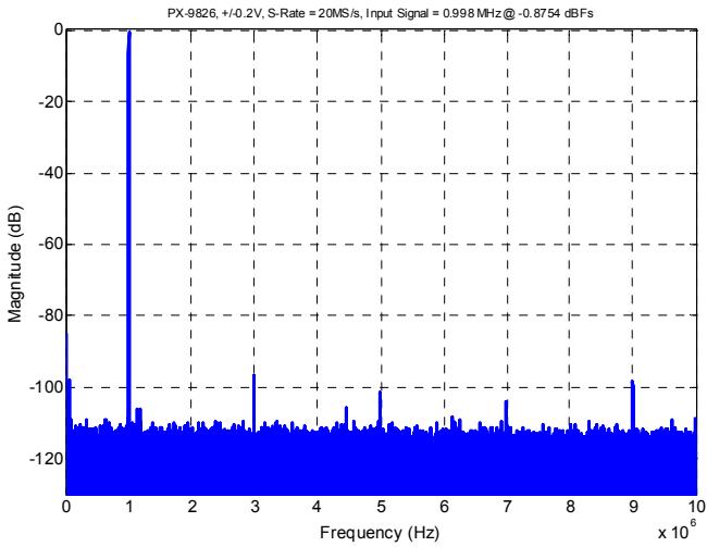
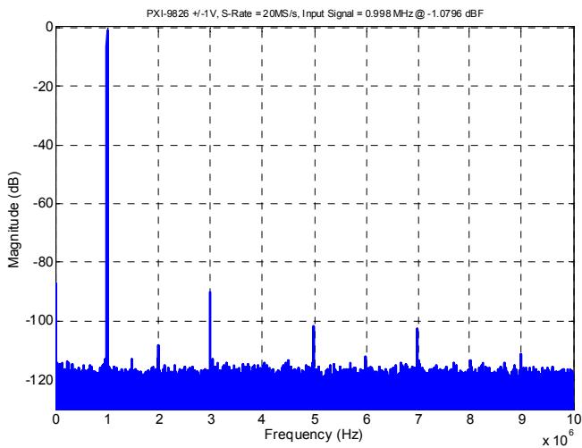
Spectral Characteristics – PXI-9826

<table><tr><td rowspan="2">Specification</td><td colspan="2">Input Range</td></tr><tr><td>±1 V</td><td>±0.2 V</td></tr><tr><td>Signal to Noise and Distortion (SINAD), typical</td><td>78.63 dBc</td><td>74.44 dBc</td></tr><tr><td>Signal-to-Noise Ratio (SNR), typical</td><td>79.95 dBc</td><td>74.48 dBc</td></tr><tr><td>Total Harmonic Distortion (THD), typical</td><td>-88.29 dBc</td><td>-93.52 dBc</td></tr><tr><td>Spurious Free Dynamic Range (SFDR), typical</td><td>88.88dBc</td><td>95.52 dBc</td></tr><tr><td>Effective Number of Bit (ENOB), typical</td><td>12.77-Bit</td><td>12.07-Bit</td></tr><tr><td colspan="3">Test Conditions: Input signal frequency is 0.998 MHz. Digitizer sampling rate at 20 MHz with 50 Ω input impedance. Calculated with 64 K-point data. Note that these dynamic parameters may vary from one unit to another, with input frequency and with the full scale input range selected.</td></tr></table>

Table 1-6: Spectral Characteristics – PXI-9826
![| Frequency (Hz) | Magnitude (dB) |\n| -------------- | -------------- |\n| 0              | -100           |\n| 1              | 0              |\n| 2              | -100           |\n| 3              | -100           |\n| 4              | -100           |\n| 5              | -100           |\n| 6              | -100           |\n| 7              | -100           |\n| 8              | -100           |\n| 9              | -100           |\n| 10             | -100           |](.pxi-98x6-50-17031-1020-001/e88ace7503d3d5304021dc202db3921ea97a729503c9f07445cb4ad36d34c936.jpg)

Figure 1-6: PXI-9826 FFT with ±0.2 V Input Range
![| Frequency (Hz) | Magnitude (dB) |\n| -------------- | -------------- |\n| 0              | -120           |\n| 1              | 0              |\n| 2              | -100           |\n| 3              | -100           |\n| 4              | -100           |\n| 5              | -100           |\n| 6              | -100           |\n| 7              | -100           |\n| 8              | -100           |\n| 9              | -100           |\n| 10             | -100           |](.pxi-98x6-50-17031-1020-001/b4a09ffed0e2607c7d7aa1f9a89fc1b8306d74aa2b339340a58cffca4a9006ae.jpg)

Figure 1-7: PXI-9826 FFT with ±1 V Input Range

Spectral Characteristics – PXI-9846

<table><tr><td rowspan="2">Specification</td><td colspan="2">Input Range</td></tr><tr><td>±1 V</td><td>±0.2 V</td></tr><tr><td>Signal to Noise and Distortion (SINAD), typical</td><td>76.06 dBc</td><td>71.97 dBc</td></tr><tr><td>Signal-to-Noise Ratio (SNR), typical</td><td>76.17 dBc</td><td>71.98 dBc</td></tr><tr><td>Total Harmonic Distortion (THD), typical</td><td>-90.65 dBc</td><td>-95.78 dBc</td></tr><tr><td>Spurious Free Dynamic Range (SFDR), typical</td><td>91.62 dBc</td><td>96.15 dBc</td></tr><tr><td>Effective Number of Bit (ENOB), typical</td><td>12.34-Bit</td><td>11.66-Bit</td></tr><tr><td colspan="3">Test Conditions: Input signal frequency is 0.998 MHz. Digitizer sampling rate at 40 MHz with 50 Ω input impedance. Calculated with 64 K-point data. Note that these dynamic parameters may vary from one unit to another, with input frequency and with the full scale input range selected.</td></tr></table>

Table 1-7: Spectral Characteristics – PCI/PXI-9846
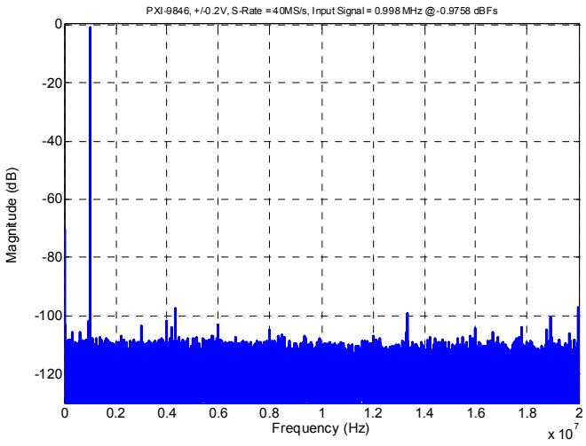
![| Frequency (Hz) | Magnitude (dB) |\n| -------------- | -------------- |\n| 0              | 0              |\n| 0.2            | -100           |\n| 0.4            | -100           |\n| 0.6            | -100           |\n| 0.8            | -100           |\n| 1.0            | -100           |\n| 1.2            | -100           |\n| 1.4            | -100           |\n| 1.6            | -100           |\n| 1.8            | -100           |\n| 2.0            | -100           |](.pxi-98x6-50-17031-1020-001/afc359e8a79f6aa38ca661f13d1c6fbd6e1f952d0b5b9c735f1c178ce6a1f8eb.jpg)

Figure 1-8: PXI-9846 FFT with ±0.2 V Input Range
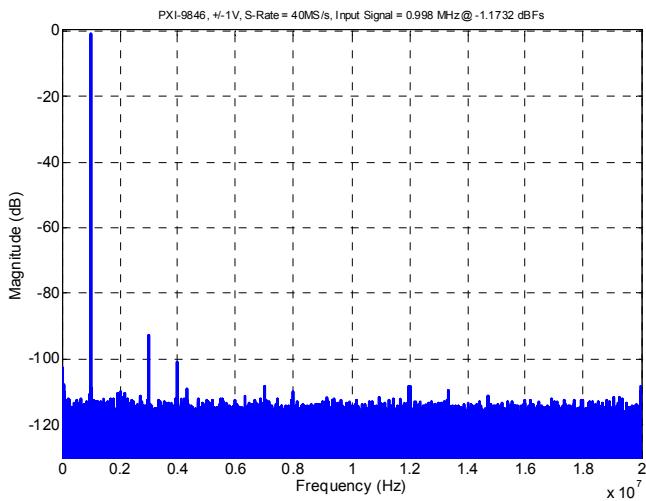
![| Frequency (Hz) | Magnitude (dB) |\n| -------------- | -------------- |\n| 0.0            | 0              |\n| 0.2            | -100           |\n| 0.4            | -100           |\n| 0.6            | -100           |\n| 0.8            | -100           |\n| 1.0            | -100           |\n| 1.2            | -100           |\n| 1.4            | -100           |\n| 1.6            | -100           |\n| 1.8            | -100           |\n| 2.0            | -100           |](.pxi-98x6-50-17031-1020-001/8b89c95aee24ce25837f79c4447428e4830e5556112f8f76fda6c8e02526c5ff.jpg)

Figure 1-9: PXI-9846 FFT with ±1 V Input Range

Timebase

<table><tr><td>Specification</td><td colspan="3">Value</td></tr><tr><td rowspan="2">Sample Clock Sources</td><td colspan="3">Internal: onboard oscillator</td></tr><tr><td colspan="3">External: CLK IN (front panel SMB connector), PXI STAR, PXI Trigger Bus[0..7], PXI 10MHz, SSI bus</td></tr><tr><td></td><td>PCI/PXI-9816</td><td>PCI/PXI-9826</td><td>PCI/PXI-9846</td></tr><tr><td>Timebase Frequency Range</td><td>10 MHz-1 MHz</td><td>20 MHz-1 MHz</td><td>40 MHz-1 MHz</td></tr><tr><td>Sampling Rate Range (24-bit divided counter)</td><td>10 MS/s-0.596 S/s</td><td>20 MS/s-1.192 S/s</td><td>40 MS/s-2.384 S/s</td></tr><tr><td>Internal Oscillator Stability</td><td colspan="3">±25 ppm</td></tr><tr><td colspan="4">CLK IN (external clock from front panel)</td></tr><tr><td>Connector Type</td><td colspan="3">SMB</td></tr><tr><td>Clock Type</td><td colspan="3">Sine wave or square wave</td></tr><tr><td>Input Impedance</td><td colspan="3">50 Ω</td></tr><tr><td>Input Coupling</td><td colspan="3">AC</td></tr><tr><td>Input Range</td><td colspan="3">1VP-P to 2VP-P</td></tr><tr><td>Overvoltage Protection</td><td colspan="3">2.5  $V_{P-P}$ </td></tr></table>

Table 1-8: Timebase

Triggering

<table><tr><td>Specification</td><td>Value</td></tr><tr><td>Trigger Sources</td><td>Software, TRG IO (front panel SMB connector), analog trigger from CH0~CH3, PXI STAR, PXI Trigger Bus[0..7], SSI bus</td></tr><tr><td>Trigger Modes</td><td>Pre-trigger, Post-trigger, Middle-trigger, Delay-trigger</td></tr><tr><td colspan="2">TRG IO, as input port</td></tr><tr><td>Connector type</td><td>SMB</td></tr><tr><td>Compatibility</td><td>3.3 V LVTTL, 5 V tolerant</td></tr><tr><td>Input Level</td><td>High threshold ( $V_{IH}$ ): 2.0 V, minimumLow threshold ( $V_{IL}$ ): 0.8 V, maximum</td></tr><tr><td>Maximum Input Overload</td><td>-0.5 V to +5.5 V</td></tr><tr><td>Trigger Polarity</td><td>Rising edge or falling edge, software programmable</td></tr><tr><td>Minimum Pulse Width</td><td>20 ns</td></tr><tr><td colspan="2">TRG IO, as output port</td></tr><tr><td>Connector Type</td><td>SMB</td></tr><tr><td>Compatibility</td><td>3.3 V TTL</td></tr><tr><td>Output Level</td><td>High threshold (VOH): 2.4V, minimumLow threshold (VOL): 0.2, maximum</td></tr><tr><td>Driving Capability</td><td>8 mA</td></tr><tr><td>Minimum Output Pulse Width</td><td>20 ns</td></tr><tr><td colspan="2">Analog Trigger</td></tr><tr><td>Sources</td><td>AI channel 0 - 3</td></tr><tr><td>Trigger Slope</td><td>Rising or falling, software selectable</td></tr><tr><td>Trigger Level Range</td><td>Full scale input range</td></tr><tr><td>Trigger Level Resolution</td><td>8-bit, 256 steps in full scale range</td></tr></table>

Table 1-9: Triggering

Data Storage and Transfer

<table><tr><td>Specification</td><td>Value</td></tr><tr><td>Onboard Memory Size</td><td>512 MB, share for four channels</td></tr><tr><td>Data Transfer</td><td>Scatter-gather DMA</td></tr></table>

Table 1-10: Data Storage and Transfer

Onboard Reference

<table><tr><td>Specification</td><td>Value</td></tr><tr><td>Onboard Reference Voltage</td><td>5 V</td></tr><tr><td>Temperature Drift</td><td>±3 ppm/°C</td></tr><tr><td>Recommended Warm-up Time</td><td>15 minutes</td></tr></table>

Table 1-11: Onboard Reference

General Information

<table><tr><td>Specification</td><td colspan="3">Value</td></tr><tr><td colspan="4">Environment</td></tr><tr><td>Operating Environment</td><td colspan="3">Ambient temperature:0°C to +55°C for PXI version,0°C to +50°C for PCI versionRelative humidity: 10% to 90%, non-condensing</td></tr><tr><td>Storage Environment</td><td colspan="3">Ambient temperature: -20°C to +85°CRelative humidity: 10% to 90%, non-condensing</td></tr><tr><td colspan="4">Physical</td></tr><tr><td>PCB Dimension(not including connectors)</td><td colspan="3">PXI version: Single 3U PXI module, 100 mm by 160 mmPCI version: Standard height, half length PCI card, 167.64 mm by 106.68 mm</td></tr><tr><td>PCI Slot Width</td><td colspan="3">1-slot</td></tr><tr><td colspan="4">PCI Bus Interface</td></tr><tr><td>PCI Signaling</td><td colspan="3">Support 3.3 V and 5 V signaling</td></tr><tr><td>PCI Interface</td><td colspan="3">32-bit, 66 MHz</td></tr><tr><td colspan="4">Electromagnetic Compatibility</td></tr><tr><td>Emission</td><td colspan="3">EN 55022</td></tr><tr><td>Immunity</td><td colspan="3">EN 55024</td></tr><tr><td colspan="4">Typical Power Requirements</td></tr><tr><td></td><td>PCI/PXI-9816</td><td>PCI/PXI-9826</td><td>PCI/PXI-9846</td></tr><tr><td>+12 V</td><td>0.3 A</td><td>0.3 A</td><td>0.3 A</td></tr><tr><td>+5 V</td><td>1.4 A</td><td>1.5 A</td><td>2.0 A</td></tr><tr><td>+3.3 V</td><td>0.8 A</td><td>0.8 A</td><td>0.8 A</td></tr><tr><td>Total Power</td><td>13.2 W</td><td>13.7 W</td><td>16.2 W</td></tr></table>

Table 1-12: General Information

# 2 Getting Started

This chapter describes the proper installation environment, installation procedures, its package contents and basic information user should be aware of.

NOTE:

Diagrams and images of equipment mentioned are used for reference only. Actual system configuration and specs may vary.

# 2.1 Installation Environment

Whenever unpacking and preparing to install any equipment described in this manual, please refer to the Important Safety Instructions chapter of this manual.

Only install equipment in well lit areas on flat, sturdy surfaces with access to basic tools such as flat and cross head screwdrivers, preferably with magnetic heads as screws and standoffs are small and easily misplaced.

# Recommended Installation Tools

 Philips (cross-head\_ screwdriver
 Flat-head screwdriver
 Anti-static wrist strap
 Anti-static mat

The PCI/PXI-9816/26/46 contain several electro-static sensitive components that can be easily be damaged by static electricity. The equipment should be handled on a grounded anti-static mat and the operator should wear an anti-static wristband during the unpacking and installation procedure.

Please also inspect the components for apparent damage. Improper shipping and handling may cause damage to the components. Be sure this is no shipping and handling damage on the components before continuing.

CAUTION

The equipment must be protected from static discharge and physical shock. Never remove any of the socketed parts except at a static-free workstation. Use the antistatic bag shipped with the product to handle the equipment and wear a grounded wrist strap when servicing.

# 2.2 Package Contents

Before continuing, check the package contents for any damage and check if the following items are included in the packaging:

 PCI/PXI-9816/26/46 digitizer card
 ADLINK All-in-one CD.
 Software installation guide
 PCI/PXI-9816/26/46 User’s Manual.

# CAUTION

Do not install or apply power to equipment that is damaged or if there is missing/incomplete equipment. Retain the shipping carton and packing materials for inspection. Please contact your ADLINK dealer/vendor immediately for assistance. Obtain authorization from your dealer before returning any product to ADLINK.

# 2.3 Mechanical Drawing and I/O Connectors
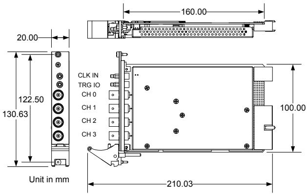
![160.00\n20.00\n122.50\n130.63\nUnit in mm\nCLK IN\nTRG IO\nCH 0\nCH 1\nCH 2\nCH 3\n100.00\n210.03](.pxi-98x6-50-17031-1020-001/dc7fff418344c8c6182b2bb6bcfee9f8f311dc1b41006414190f10dc668a2d9c.jpg)

Figure 2-1: PXI-98x6 Mechanical Drawing
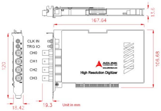
![167.64\n13.6\n120\n18.42\n19.3\nUnit in mm\nADLINK\nwww.adlink.com\nHigh Resolution Digitizer](.pxi-98x6-50-17031-1020-001/59b2e04a21626a1e7afc93a2ef6cb5155a96da72345f579af559cc8d8820a756.jpg)

Figure 2-2: PCI-98x6 Mechanical Drawing

The ADLINK PXI-9816/PXI-9826/PXI-9846 is packaged in a Eurocard form factor with PXI specifications measuring 160 mm in length and 100 mm in height (not including connectors). The PCI-9816/9826/9846 is a half-length and standard height PCI form factor. Please refer to above figure for detail dimension.

The connector types and functions are described as follows.

<table><tr><td>Connector</td><td>Direction</td><td>Type</td><td>Description/Function</td></tr><tr><td>CLK IN</td><td>Input</td><td>SMB</td><td>The CLK IN is a 50Ω, AC-coupled external timebase input.</td></tr><tr><td>TRG IO</td><td>Input Output</td><td>SMB</td><td>The TRG IO is a bidirectional port for external digital trigger input or output.</td></tr><tr><td>CH0</td><td rowspan="4">Input</td><td rowspan="4">BNC</td><td rowspan="4">These channels are for attaching the analog input signals.</td></tr><tr><td>CH1</td></tr><tr><td>CH2</td></tr><tr><td>CH3</td></tr></table>

Table 2-1: Connector Pin Assignments

# 2.4 Installing the module

To install the PXI-9816/PXI-9826/PXI-9846 module:

1. Turn off the PXI system/chassis and disconnect the power plug from the power source.
2. Align the module’s edge with the card guide in the PXI chassis.
3. Slide the module into the chassis, until resistance is felt from the PXI connector.
4. Push the ejector upwards and fully insert the module into the chassis.
5. Once inserted, a “click” can be heard from the ejector latch.
6. Tighten the screw on the front panel.
7. Power on the PXI system/chassis.

To remove the module, reverse step 2 through 6 above.

To install the PCI-9816/PCI-9826/PCI-9846 module:

1. Turn off your computer
2. Remove the top cover of your computer
3. Select an available PCI slot and remove the bracketretaining screw and the bracket cover.
4. Line up the PCI digitizer with the PCI slot on the back panel. Slowly push down on the top of the PCI digitizer until its card-edge connector is resting on the slot receptacle.
5. Reinstall the bracket-retaining screw to secure the PCI digitizer to the back panel rail.
6. Restore the computer cover.

# 2.5 Software Support

ADLINK provides comprehensive software drivers and packages to suit various user approaches to building a system. Aside from programming libraries, such as DLLs, for most Windows-based systems, ADLINK also provides drivers for other application environment such as LabVIEW® and MATLAB®. ADLINK also provides ActiveX component ware for measurement and SCADA/ HMI, and breakthrough proprietary software applications.

All software options are included in the ADLINK All-in-One CD.

# 2.5.1 Driver Support for Windows

# DAQPilot

DAQPilot is a driver and SDK with a graphics-driven interface for various application development environments. DAQPilot comes as ADLINK's commitment to provide full support to its comprehensive line of data acquisition products and is designed for the novice to the most experienced programmer.

As a task-oriented DAQ driver, SDK and wizard for Windows systems, DAQPilot helps you shorten the development time while accelerating your learning curve for data acquisition programming.

![DAQPilot\nANALOG INPUT\nANALOG OUTPUT\nDIGITAL INPUT\nDIGITAL OUTPUT\nTIMER/CTR\nYour pilot to\ndata acquisition world\nADLINK\nTECHNOLOGY INC.\nCopyright © 2007 ADLINK Technology Inc. All Rights Reserved.](.pxi-98x6-50-17031-1020-001/dd8a6ffd1e2d1c1fb3d9f8287d55d6c5adf875de345583623b6beb86d8ba86ad.jpg)

Figure 2-3: DAQPilot Main Interface

You can download and install DAQPilot at:

http://www.adlinktech.com/TM/DAQPilot.html

# DAQMaster

The ADLINK DAQMaster is a smart device manager that opens up access to ADLINK data acquisition and test and measurement products. DAQMaster delivers all-in-one configurations and provides you with a full support matrix to properly and conveniently configure ADLINK Test and Measurement products.

As a configuration-based device manager for ADLINK DAQ cards, DAQMaster enables you to manage ADLINK devices and interfaces, install and upgrade software applications, and manage ADLINK DAQPilot tasks.

![DAQMaster\nFile Options Yew Help\nDevice Manager\nSoftware Manager\nTask Manager\nProducts\nADLINK Test & Measurement\nDevice Overview/Support Matrix\n# Type Model Form Factor Driver ComponentWare\nPCI LPCePCe P0 Windows Linux DAOBench ComponentWare\n1 Analog Output Modules 8008R216 v v PCS-DSAX PCS-DSAXK V PCS-OCX\n2 6306 v PCS-DSAX PCS-DSAXK V PCS-OCX\n3 7200 v PCS-DSAX PCS-DSAXK V PCS-OCX\n4 7224 v PCS-DSAX PCS-DSAXK V PCS-OCX\n5 7230 v PCS-DSAX PCS-DSAXK V PCS-OCX\n6 7233 v PCS-DSAX PCS-DSAXK V PCS-OCX\n7 7234 v PCS-DSAX PCS-DSAXK V PCS-OCX\n8 7248 v PCS-DSAX PCS-DSAXK V PCS-OCX\n9 7249 v PCS-DSAX PCS-DSAXK V PCS-OCX\n10 7263 v PCS-DSAX PCS-DSAXK V PCS-OCX\n11 7252 v PCS-DSAX PCS-DSAXK V PCS-OCX\n12 7256 v PCS-DSAX PCS-DSAXK V\n13 7258 v PCS-DSAX PCS-DSAXK V\n14 Digital IO Modules 7260 v PCS-DSAX PCS-DSAXK V\n15 7266 v PCS-DSAX PCS-DSAXK V PCS-OCX\n16 7300 v PCS-DSAX PCS-DSAXK V PCS-OCX\n17 7432 v PCS-DSAX PCS-DSAXK V PCS-OCX\n18 7433 v PCS-DSAX PCS-DSAXK V PCS-OCX\n19 7434 v PCS-DSAX PCS-DSAXK V PCS-OCX\n20 7442 v PCS-DSAX PCS-DSAXK V\n21 7443 v PCS-DSAX PCS-DSAXK V\n22 7444 v PCS-DSAX PCS-DSAXK V\n23 7452 v PCS-DSAX PCS-DSAXK V\n24 7349 v PCS-DSAX PCS-DSAXK V PCS-OCX\n25 7396 v PCS-DSAX PCS-DSAXK V PCS-OCX\n26 Digitizer Modules 9010MWTZ v PCU-DASAK PCU-DASAK V PCU-DASCK\n27 Product Support Matrix WD-DASAK WD-DASAK WD-DASCK\n3rd Party Support & Application\nDevice Manager(Installed) Drag the selected device item to subfunction button to launch\nCalibrates DAQ-2000 series modules](.pxi-98x6-50-17031-1020-001/806c4b4ce21ac8049e61390552a6d29d0fbd5910e700cd9c4e1a56d857b9ee8b.jpg)

Figure 2-4: DAQMaster Device Manager

# 2.5.2 WD-DASK (Legacy Drivers and Support)

WD-DASK is composed for advanced 32-bit kernel drivers for customized DAQ application development. WD-DASK enables you to perform detailed operations and achieve superior performance and reliability from your digitizer system. DASK kernel drivers now support the revolutionary Windows Vista OS.

![Based on the provided image, here is the description of the flowchart/block diagram:\n\n**User Mode (Left Side)**\n*   **Labeled Blocks:** A vertical column of blue rectangles lists programming languages/environments: 'Delphi', 'BCB', 'VC++', 'VB', 'VB.NET', and 'C#'.\n*   **Interface Blocks:** Three teal oval blocks are positioned between the language column and the kernel boundary:\n    *   'PCIS-DASK'\n    *   'D2K-DASK'\n    *   'WD-DASK'\n*   **Connections:** Orange arrows point from each of these teal ovals to the right, towards the 'System Service' bar.\n\n**Kernel Mode (Center)**\n*   **System Service:** A vertical blue rounded rectangle labeled 'System Service' receives the arrows from the user mode.\n*   **DASK Kernel Driver:** To the right of 'System Service' is a large grid structure. Red text labels this section 'DASK Kernel Driver (.sys)'. The grid contains the following sub-blocks:\n    *   'Process Structure'\n    *   'Object Manager'\n    *   'Memory Manager'\n    *   'Executive Support'\n    *   'Configuration Manager'\n    *   'Plug and Pay'\n    *   'Power Manager'\n    *   'I/O Manager'\n    *   'File System'\n    *   'Lowest-level Driver'\n\n**Hardware Layer (Right Side)**\n*   **Labeled Blocks:** Two vertical blue rounded rectangles stand to the right of the kernel section:\n    *   'Hardware Abstraction Layer'\n    *   'Hardware'\n*   **Connections:** Two orange arrows point from the 'Hardware Abstraction Layer' to the 'Hardware' block.](.pxi-98x6-50-17031-1020-001/17b741d94e565467a759506fe6f95fd2a9d44b7aa3d400a315154751ede8a0a3.jpg)

Figure 2-5: Legacy Software Support Overview

# 3 Operation Theory

The operation theory of the PCI/PXI-9816/26/46 is described in this chapter, including the control and setting of signal sources, trigger sources, trigger modes, data transfers, and synchronizing multiple modules.

# 3.1 Functional Block Diagram

![**Labeled Blocks:**\n*   CLK IN\n*   TRG IO\n*   Analog Trigger Circuit\n*   Timing Control\n*   Trigger Routing\n*   PXI Trigger Bus(7..0)\n*   PXI Trigger Bus\n*   PXI STAR Trigger\n*   PXI 10MHz CLK\n*   CH0\n*   CH1\n*   CH2\n*   CH3\n*   Analog Input Path\n*   16-bit ADC\n*   Memory\n*   PXI-98X6 Local Bus Controller\n*   PCI Controller\n*   PCI Bus\n*   Calibration Circuit\n*   Precision Reference Source\n*   32-bit/66MHz (Label)\n\n**Connections:**\n*   **CLK IN** connects to **Timing Control** and **Trigger Routing**.\n*   **TRG IO** connects to **Timing Control**.\n*   **Timing Control** connects to **Trigger Routing**.\n*   **Trigger Routing** connects to **PXI Trigger Bus(7..0)** and **PXI STAR Trigger**.\n*   **PXI Trigger Bus(7..0)** connects to **PXI Trigger Bus**.\n*   **PXI STAR Trigger** connects to **Trigger Routing** and **Timing Control**.\n*   **PXI 10MHz CLK** connects to **Timing Control** and **Trigger Routing**.\n*   **CH0**, **CH1**, **CH2**, and **CH3** connect to respective **Analog Input Path** blocks.\n*   Each **Analog Input Path** connects to a respective **16-bit ADC**.\n*   Signal lines between the **Analog Input Path** and **16-bit ADC** connect via blue arrows to the **Analog Trigger Circuit**.\n*   Purple lines interconnect the **CH** blocks, **Analog Input Path** blocks, and the **Calibration Circuit**.\n*   **Calibration Circuit** connects to **Precision Reference Source**.\n*   The four **16-bit ADC** blocks connect to the **PXI-98X6 Local Bus Controller**.\n*   **PXI-98X6 Local Bus Controller** connects bidirectionally to **Memory**.\n*   **PXI-98X6 Local Bus Controller** connects bidirectionally to **PCI Controller**.\n*   **PCI Controller** connects to **PCI Bus** (labeled 32-bit/66MHz).](.pxi-98x6-50-17031-1020-001/a076c8ddfb1eeeb35d743693ab5deeb5bf088b403bc4b66bd7e719bf55f3d78a.jpg)

Figure 3-1: PXI-98x6 Functional Block Diagram
![This block diagram illustrates a data acquisition system architecture with analog inputs, digital processing, and bus interfaces.\n\n**Labeled Blocks:**\n*   **Inputs/Connectors:** CLK IN, TRG IO, CH0, CH1, CH2, CH3.\n*   **Analog Processing:** Analog Input Path (repeated four times), 16-bit ADC (repeated four times), Analog Trigger Circuit, Calibration Circuit, Precision Reference Source.\n*   **Control/Logic:** Timing Control, Trigger Routing.\n*   **Controller/Data Path:** PCI-98X6 Local Bus Controller, Memory, PCI Controller.\n*   **Buses/Outputs:** SXI Bus, PCI Bus (labeled with 32-bit/66MHz).\n\n**Connections:**\n*   **Analog Inputs:** The inputs **CH0**, **CH1**, **CH2**, and **CH3** each connect to a respective **Analog Input Path**, which feeds into a **16-bit ADC**.\n*   **Triggering:** The **CH0** through **CH3** channels also feed into the **Analog Trigger Circuit**. This circuit connects to **Timing Control** and **Trigger Routing**.\n*   **Top Inputs:** **CLK IN** connects directly to **Trigger Routing**. **TRG IO** connects to **Trigger Routing**.\n*   **Digital Processing:** The outputs from the four **16-bit ADC** blocks connect to the **PCI-98X6 Local Bus Controller**.\n*   **Calibration:** The **CH0** through **CH3** channels connect to the **Calibration Circuit**, which connects to the **Precision Reference Source**.\n*   **Controller Interactions:** The **Trigger Routing** block connects to the **PCI-98X6 Local Bus Controller** and the **SXI Bus** (bidirectional).\n*   **Bus Interfaces:** The **PCI-98X6 Local Bus Controller** connects to **Memory** and the **PCI Controller**. The **PCI Controller** connects to the **PCI Bus** (bidirectional, labeled 32-bit/66MHz).](.pxi-98x6-50-17031-1020-001/9e54aefd6bf99c3509059ad5664d6807da9ebff40ae193f3ec70adf09558fe7b.jpg)

Figure 3-2: PCI-98x6 Functional Block Diagram

# 3.2 Basic AI Acquisition

In this section, we are going to explain the basic acquisition timing.

# 3.2.1 Analog Input Path

The following figure shows the block diagram of the single analog input path of a digitizer. Each path provides a choice of 50 Ω input impedance or high impedance. The gain amplifier is optimized for each input range with low noise and high dynamic range. An antialiasing filter is also adopted to eliminate high frequency noise. The 16-bit ADC provides not only accurate DC performance but also high signal-to-noise ratio, high spurious-free dynamic range in AC performance.

![The diagram illustrates a signal processing chain starting from the left and moving to the right.\n\n**Blocks and Sequence:**\n1.  **Input Connector:** An unlabeled connector symbol on the far left.\n2.  **Protection Circuitry:** Connected directly from the input.\n3.  **Junction:** A node after the protection circuitry where the path splits.\n4.  **Hi Impedance Buffer:** Connected to the main path from the junction.\n5.  **Gain Amplifier:** Connected from the buffer.\n6.  **Anti-aliasing Filter:** Connected from the amplifier.\n7.  **16-bit 40M/20M/10M ADC:** Connected from the filter.\n8.  **Onboard Memory:** Connected from the ADC.\n9.  **PCI Interface:** The final block connected from the memory.\n\n**Side Connections from the Junction:**\n*   **Upward Path:** Connects to a light blue rectangular block, which leads to a label box reading '**Calibration Source**'.\n*   **Downward Path:** Connects to a switch symbol. The switch connects to a resistor labeled '**500**' which leads to a ground symbol.](.pxi-98x6-50-17031-1020-001/f133b5f679e70b787eea4a46792071a3490bb3b168d1760c3cbcb9262e95e69e.jpg)

Figure 3-3: Analog Input Signal Block Diagram

# 3.2.2 Basic Acquisition Timing

The trigger is a signal that starts or stops the acquisition. In posttrigger mode and delay trigger mode, the trigger is used to initiate acquisition. In pre-trigger mode, the trigger is used to stop acquisition. In middle-trigger mode, the trigger is used to inform the acquisition engine to acquire the specific number of data and then stop.

Timebase is a clock that sent to the ADC of each channel and the acquisition engine for essential timing functionality. The source of timebase can be either internal oscillator or external clock generator. Usually the maximum sampling rate of a digitizer is determined by the speed of timebase. However, other sampling rate can be achieved by specifying a scan interval counter. Please refer to Table 3-1 below and Section “3.3.4” on page 32 for more details.

Table 3-1 shows several basic counters required for operating digitizers.

<table><tr><td>Counter Name</td><td>Length</td><td>Valid value</td><td>Description</td></tr><tr><td>ScanIntrv</td><td>24-bit</td><td>1 - 16777215</td><td>Scan Interval CounterThis counter is a TIMEBASE divider to the achieve equivalent sampling rate of digitizer. The equation is:Sampling rate = TIMEBASE / ScanIntrvThe value of TIMEBASE depends on the card type. Take the PCI/PXI-9846 (40 MS/s) as an example, ScanIntrv = 1 results in 40 MS/s and ScanIntrv = 2 results in 20 MS/s, and so on.</td></tr><tr><td>DataCnt</td><td>29-bit</td><td>1 - 536870911</td><td>Data CounterYou can specify the amount of data to be acquired. The digitizer equips 512MB memory to store acquired data.</td></tr><tr><td>trigDelayTicks</td><td>32-bit</td><td>1 - 536870911</td><td>Delay Trigger CounterThe delay trigger counter is used to indicate the time between a trigger event and the start of an acquisition. The unit of a delay count is the period of the TIMEBASE. For PCI/PXI-9816, the unit is 100ns and for PCI/PXI-9846 the unit is 25ns. Refer to section 3.5.4 for more detail.</td></tr><tr><td>ReTrgCnt</td><td>24-bit</td><td>1 - 16777215</td><td>Re-Trigger CounterThe digitizer can enable re-trigger to accept multiple triggers. Refer to section 3.5.5 for more detail.</td></tr></table>

# Table 3-1: Basic Counters

Refer to Figure 3-4 and use post trigger mode as an example. When a trigger is accepted by digitizer, the acquisition engine of the digitizer will begin to acquire data that coming from ADC and store these sampled data to onboard memory. The sampled data is generated continuously at the rising edge of timebase according to the scan interval counter setting. While sampled data reaches customer specified number, in this example is 256, the acquisition ends. Once the acquisition ends, acquisition engine begins to send request to system and transfer data from onboard memory back to system by DMA.

![Based on the provided image, here is an accurate and concise description of the flowchart/block diagram:\n\n**Labeled Blocks and Signals:**\n*   **Analog signal**: A sine-like waveform at the top.\n*   **TIMEBASE**: A square wave clock signal below the analog signal.\n*   **Trigger**: A pulse signal that goes high and then low.\n*   **Acquisition In Progress**: A signal line that goes high.\n*   **DATA**: A sequence of hexagonal blocks labeled 'D1', 'D2', 'D3', 'D4', followed by ellipses, and ending with 'D253', 'D254', 'D255', 'D256'.\n*   **Text Annotation**: 'Acquisition starts right after this clock edge'.\n*   **Footer Text**: 'Trigger mode = post-trigger, DataCnt = 256, ScanIntrv = 1'.\n\n**Connections and Relationships:**\n*   **Sampling**: The rising edges of the **TIMEBASE** align vertically with dots on the **Analog signal**, indicating the moments when the signal is sampled.\n*   **Triggering**: The **Trigger** signal transitions high and then low.\n*   **Acquisition Start**: The **Acquisition In Progress** signal goes high. An arrow connects the text 'Acquisition starts right after this clock edge' to the first rising edge of the **TIMEBASE** after the acquisition phase begins.\n*   **Data Sequence**: The **DATA** blocks correspond to the **TIMEBASE** rising edges. 'D1' aligns with the first rising edge of the second group of clocks (after the gap), indicating the start of data capture. The sequence continues to 'D256'.](.pxi-98x6-50-17031-1020-001/ebcd3f0c18459ac2fa61bc6942c7af8af42014eecfce087178f10cb7d8f690dd.jpg)

Figure 3-4: Basic Acquisition Timing Of Digitizer

# 3.2.3 AI Data Format

The following table illustrates the idea transfer characteristics of various input ranges of the PCI/PXI-9816/26/46. The data format of the PCI/PXI-9816/26/46 is straight binary.

<table><tr><td>Description</td><td colspan="2">Analog Input Range</td><td>Digital Code (HEX)</td></tr><tr><td>Full-scale Range</td><td>±1 V</td><td>±0.2 V</td><td></td></tr><tr><td>Least significant bit</td><td>30.52 μV</td><td>6.10 μV</td><td></td></tr><tr><td>FSR – 1LSB</td><td>0.999969 V</td><td>0.199993 V</td><td>FFFF</td></tr><tr><td>Midscale + 1LSB</td><td>30.5 μV</td><td>6.10 μV</td><td>8001</td></tr><tr><td>Midscale</td><td>0.0 V</td><td>0.0 V</td><td>8000</td></tr><tr><td>Midscale - 1LSB</td><td>-30.5 μV</td><td>-6.10 μV</td><td>7FFF</td></tr><tr><td>-FSR</td><td>-1.000 V</td><td>-0.200 V</td><td>0000</td></tr></table>

Table 3-2: AI Data Format

# 3.3 ADC Sampling Rate and TIMEBASE Control

The PXI/PCI-98X6 supports several timebase sources for analog input conversion:

 Internal oscillator
 External clock through front panel
 PXI\_STAR (PCI version)
 PXI Trigger Bus[0..7] (PXI version)
 PXI 10M (PXI version)
 SSI (PCI version)

The following diagram shows the timebase architecture of the PXI/ PCI-98X6.

![**Labeled Blocks:**\n*   Onboard Oscillator\n*   Ext. CLK IN SMB Connector\n*   CLK Buffer\n*   PXI Interface\n*   PXI Trigger Bus(0:7)\n*   8-to-1 MUX (bottom left)\n*   Timebase Clock Mux\n*   1-to-5 Clock Buffer\n*   8-to-1 MUX (top right)\n*   ADC0, ADC1, ADC2, ADC3\n*   PXI Trigger Bus or SSI\n\n**Connections:**\n*   **Ext. CLK IN SMB Connector** connects to **CLK Buffer**.\n*   **CLK Buffer** connects to **Timebase Clock Mux**.\n*   **Onboard Oscillator** connects to **Timebase Clock Mux**.\n*   **PXI Interface** connects to a line labeled **PXI_STAR**, which connects to **Timebase Clock Mux**.\n*   **PXI Interface** connects to a line labeled **PXI_10M**, which connects to **Timebase Clock Mux**.\n*   **PXI Interface** connects to a path labeled **PXI Trigger Bus(0:7)**, which connects to the bottom **8-to-1 MUX**, which then connects to **Timebase Clock Mux**.\n*   **Timebase Clock Mux** connects to **1-to-5 Clock Buffer**.\n*   **1-to-5 Clock Buffer** splits into four outputs connecting to **ADC0**, **ADC1**, **ADC2**, and **ADC3**.\n*   **1-to-5 Clock Buffer** also connects to the top **8-to-1 MUX**, which connects to **PXI Trigger Bus or SSI**.](.pxi-98x6-50-17031-1020-001/ce709849605b3fae8bd1d71658c05507ae8f244d3cc4f53aa8b9258c97ccff0b.jpg)

Figure 3-5: PCI/PXI-98x6 Timebase Source and Architecture.

# 3.3.1 Internal Oscillator

The PCI/PXI-9816/26/46 equips a high stability, low jitter oscillator for the ADCs. The oscillators are 10 MHz, 20 MHz and 40 MHz for PCI/PXI-9816, PCI/PXI-9826 and PCI/PXI-9846, respectively.

# 3.3.2 External Clock Through Front Panel

When you need a specific timebase in some applications that the onboard oscillator is not achievable, a clock from an external device can replace onboard oscillator. In addition, external timebase also provides a method to synchronize digitizers to other measurement modules by distributing/receiving a common clock to/from multiple modules. The PCI/PXI-9816/26/46 can receive an external timebase from the front panel connector (CLK IN), PXI STAR or one of the PXI Trigger Bus lines.

You can supply the timebase from external SMB connector CLK IN, which should be a sine wave or square wave signal. This signal is AC coupled with 50 Ω input impedance and the valid input level is from 1 to 2 volts peak-to-peak. Note that the external clock must be continuous for correct ADC operation because of the pipeline architecture of the ADC.

# 3.3.3 External Clock from PXI Interfaces

The PCI/PXI-9816/26/46 can receive timebase via one of the PXI Trigger Bus lines by software selection. The eight PXI Trigger Bus lines (PXI\_TRIG[0..7]) provide inter-module synchronization and communication. Note that this function is only available when the PCI/PXI-9816/26/46 is in a PXI system. It’s not supported when PCI/PXI-9816/26/46 is in a CompactPCI system.

When the PCI/PXI-9816/26/46 is plugged into a generic peripheral slot in a PXI system, it can receive timebase from PXI\_STAR. The PXI\_STAR signal comes from star trigger controller is matched in propagation delay within 1 ns and the delay from star trigger slot to peripheral slot is less than 5 ns. According these hardware features, the PCI/PXI-9816/26/46 can achieve very good synchronization performance when using PXI\_STAR as timebase clock source. Note that the function is only available when the PCI/PXI-98x6 is in a PXI system. It’s not supported when the PCI/PXI-9816/26/46 is in a CompactPCI system.

# 3.3.4 Sampling Rate Control

By specifying different scan interval counter (24-bit) value, different sampling rate can be achieved. The following formula determines the ADC sampling rate.

Sampling Rate = TIMEBASE / ScanIntrv

Where ScanIntrv is scan interval counter, value can be 1, 2, 3, 4… $2 ^ { 2 4 } - 1$ .

Refer to Figure 3-6 for detail timing.

![This timing diagram illustrates signal relationships and data acquisition timing.\n\n**Top Signals:**\n*   **Trigger:** A signal labeled 'Trigger' goes high immediately after the first clock edge and returns low immediately after the tenth clock edge.\n*   **TIMEBASE:** A signal labeled 'TIMEBASE' consists of a clock waveform with upward-pointing arrows on the rising edges.\n\n**DATA Section:**\nA vertical bracket labeled 'DATA' groups three rows representing different scan intervals:\n*   **ScanIntrv = 1:** A row containing blocks labeled 'D1' through 'D10'. Each block is aligned with a consecutive clock edge.\n*   **ScanIntrv = 2:** A row containing blocks labeled 'D1' through 'D6'. Each block is aligned with every second clock edge.\n*   **ScanIntrv = 3:** A row containing blocks labeled 'D1' through 'D4'. Each block is aligned with every third clock edge.\n\n**Bottom Annotation:**\n*   A signal line labeled 'Acquisition In Progress'.\n*   An arrow points from the text 'Acquisition starts right after this clock edge' to the first rising edge of the TIMEBASE signal.](.pxi-98x6-50-17031-1020-001/c9a3a7545e46d686a7bafb0bd7ddf56aa7036fe2a758f74909a7821c88dca229.jpg)

Figure 3-6: Configuring Different Sampling Rate of a Digitizer.

# 3.3.5 Timebase Exporting

The PCI/PXI-9816/26/46 can export timebase to one of the eight PXI trigger bus lines. By software programming, you can pick up a trigger line to transmit timebase clock. This feature is very useful when synchronize to multiple measurement modules.

# 3.4 Trigger Sources

In addition to the internal software trigger, the PCI/PXI-9816/26/46 also supports external analog triggers, external digital triggers, PXI\_STAR triggers, PXI Trigger Bus[0..7] and SSI bus.. You can configure the trigger source by software command. Please refer to Figure 3.7 for trigger architecture.

![This flowchart illustrates a trigger signal routing system.\n\n**Inputs and Pre-processing:**\n*   Four lines labeled **Analog CH0**, **Analog CH1**, **Analog CH2**, and **Analog CH3** feed into a curved arrow pointing to a triangle labeled **Analog TRG Circuit**.\n*   A **TRG IO SMB Connector** (top left) connects to the **Analog CH0** line.\n*   The **Analog TRG Circuit** outputs an **Analog Trigger** signal.\n\n**Trigger Source Multiplexing:**\n*   A large vertical block labeled **Trigger Source Mux** receives inputs from:\n    *   **Analog Trigger**\n    *   **Software Trigger**\n    *   **Digital Trigger Input**\n    *   **PXI Trigger Bus(0:7)** (a thick black line)\n*   To the left of this block, double-headed arrows indicate **PXI Interface** and **SSI Bus** (dashed line), with a note below: **(Only available in PCI version)**.\n\n**Processing and Routing:**\n*   The **Trigger Source Mux** sends a signal to a block labeled **Trigger Decision**.\n*   Below the **Trigger Decision** block are the labels **SSI_TRIG1**, **SSI_TRIG2**, and **SSI_START_OP**.\n*   The **Trigger Decision** block feeds into a large vertical block labeled **Trigger Output Mux**.\n\n**Outputs:**\n*   The **Trigger Output Mux** has three outputs:\n    1.  **To Internal Circuit** (top arrow).\n    2.  **Digital Trigger Output** (right arrow), which connects to a **TRG IO SMB Connector** (far right) with a ground symbol.\n    3.  A thick arrow pointing down/right to **PXI Interface or SSI**.](.pxi-98x6-50-17031-1020-001/b662794e7b274e65c412464699f4abbc948ee6741707b32f343d95ffa09de7c7.jpg)

Figure 3-7: PCI/PXI-98x6 Trigger Architecture

# 3.4.1 Software Trigger

Software trigger is generated by software command. The trigger asserts right after executing specified function calls to begin the operation.

# 3.4.2 External Digital Trigger

An external digital trigger occurs when a TTL rising edge or a falling edge is detected at the SMB connector TRG IO on the front panel. As illustrated in Figure 3-8, the trigger polarity can be selected by software. Note that the signal level of the external digital trigger signal should be TTL-compatible, and the minimum pulse width is 20 ns.

![Pulse Width ) 20 ns](.pxi-98x6-50-17031-1020-001/ad6e6281459ace3deffbf493c39f898ceb2e61ed8be12bef582fad66e0c6fafd.jpg)

Rising edge trigger event

![Pulse Width ) 20 ns](.pxi-98x6-50-17031-1020-001/23f8d22af0bc6f122a4964de4ca7c78dab4ef1e151e3a4db886deb4980db0bc6.jpg)

Falling edge trigger event
Figure 3-8: External Digital Trigger Polarity and Pulse Width Requirement.

# 3.4.3 Analog Trigger

You can choose either CH0, CH1, CH2 or CH3 as the trigger signal while using external analog trigger source. The trigger level can be set by software with 8-bit resolution. Please refer to Table 3-3 for the ideal transfer characteristic.

<table><tr><td>Trigger Level Setting (Hex)</td><td>Trigger Voltage (-1V to +1V Range)</td><td>Trigger Voltage (-0.2V to +0.2V)</td></tr><tr><td>0xFF</td><td>0.992V</td><td>0.1984V</td></tr><tr><td>0xFE</td><td>0.984V</td><td>0.1968V</td></tr><tr><td>---</td><td>---</td><td>---</td></tr><tr><td>0x81</td><td>0.0078V</td><td>1.56mV</td></tr><tr><td>0x80</td><td>0V</td><td>0V</td></tr><tr><td>0x7F</td><td>-0.0078V</td><td>-1.56mV</td></tr><tr><td>---</td><td>---</td><td>---</td></tr><tr><td>0x01</td><td>-0.992V</td><td>-0.1984V</td></tr></table>

Table 3-3: Ideal Transfer Characteristics for Analog Triggers

The trigger conditions for analog triggers are illustrated in Figure 3-9 and described as follows:

 Positive-slope trigger: The trigger event occurs when the trigger signal (analog input signal) changes from a voltage that is lower than the specified trigger level to a voltage that is higher than the specified trigger level.
Negative-slope trigger: The trigger event occurs when the trigger signal (analog input signal) changes from a voltage that is higher than the specified trigger level to a voltage that is lower than the specified trigger level.

![| Event Type                  | Event Description                     |\n| --------------------------- | ------------------------------------- |\n| Positive-Slope Trigger Event | Occurs                               |\n| Negative-Slope Trigger Event | Occurs                               |](.pxi-98x6-50-17031-1020-001/f40e853c72b018cc5194802e69a51bb674f51caf4c8a7438753fbb5a820ff29a.jpg)

Figure 3-9: Analog Trigger Conditions

# 3.4.4 PXI STAR Trigger

When you select PXI STAR as the trigger source, the PXI-9816/ PXI-9826/PXI-9846 can accept a TTL-compatible digital signal as a trigger signal. The trigger occurs when a rising edge or falling edge is detected at PXI STAR. You can use software to configure the trigger polarity. The minimum pulse width requirement of this digital trigger signal is 20 ns.

# 3.4.5 PXI Trigger Bus

The PXI-9816/PXI-9826/PXI-9846 utilizes PXI Trigger Bus[0..7] as System Synchronization Interface (SSI). Using the interconnected bus provided by PXI Trigger Bus, you can easily synchronize multiple modules.

When configured as input, the PXI-9816/PXI-9826/PXI-9846 is served as a slave module and can accept three different SSI signals, SSI\_TRG1, SSI\_TRG2 and SSI\_START\_OP. When configured as output, the PXI-9816/PXI-9826/PXI-9846 is served as a master module and can output SSI\_TRG1, SSI\_TRG2 or SSI\_START\_OP to PXI Trigger Bus. Each signal can be routed from one of the PXI Trigger Bus[0..7] by software programming. For more detail about these signals, please refer to Section “3.7” on page 44.

# 3.4.6 Trigger Signal Exporting

The PCI/PXI-9816/26/46 can export trigger signals to following connectors/bus: TRG IO on front panel and PXI Trigger Bus[0..7].

The TRG IO on the front panel can also be programmed to output the trigger signal when the trigger source is from software trigger, analog trigger, PXI STAR, or PXI Trigger Bus[0..7]. The timing characteristic is in Figure 3-10.

![Tw\nTRG IO\n(Output)\nTw = 2 TIMEBASE Clocks](.pxi-98x6-50-17031-1020-001/229a906f0b1b63748466876638253ce3cfb86fae7324c794c7e4e5bd38a0f9a9.jpg)

Figure 3-10: TRG IO Output Signal Timing

The PCI/PXI-9816/26/46 utilizes PXI Trigger Bus[0..7] as System Synchronize Interface. When configured as output, the PCI/PXI-9816/26/46 is served as a master module and can output 3 different trigger signals, SSI\_TRG1, SSI\_TRG2 and SSI\_START\_OP. You can route these signals to any of PXI Trigger Bus[0..7] signals via software programming.

# 3.5 Trigger Modes

There four trigger modes working with trigger sources to initiate different data acquisition timing when a trigger event occurs. They are described in this section.

# 3.5.1 Post-trigger Acquisition

Use post-trigger acquisition when you want to collect data after the trigger event, as illustrated in Figure 3-11.

![This is a timing diagram illustrating a data acquisition sequence. It consists of a horizontal time axis at the top and two signal traces below it.\n\n**Timeline and Events:**\nA horizontal line with an arrow pointing right is labeled **'Time'**. Three vertical arrows point to this timeline to mark specific events:\n1.  **'Operation start'**\n2.  **'Trigger Event Occurs'** followed by **'Acquisition start'** on the line below.\n3.  **'Acquisition stop'** followed by **'Begin to transfer data to system'** on the line below.\n\n**Signal Traces:**\n1.  **Trigger:** The upper trace is labeled **'Trigger'**. It displays a waveform that remains low until the second event, where it briefly pulses high (a square wave) and then returns to low.\n2.  **Data:** The lower trace is labeled **'Data'**. It displays a waveform that remains low until the second event, then rises to a high state forming a rectangular block labeled **'N samples'**. This block continues until the third event, where it drops back to low.](.pxi-98x6-50-17031-1020-001/0538833c95224b2031878c32fbab3daeb78c48494ff569d2099878d977735879.jpg)

Figure 3-11: Post-trigger Acquisition

# 3.5.2 Pre-trigger Acquisition

Use pre-trigger acquisition to collect data before the trigger event. The acquisition starts once specified function calls are executed to begin the pre-trigger operation, and it stops when the trigger event occurs.

If the trigger event occurs after the specified amount of data has been acquired, the system only stores the data before the trigger event with specified amount, as illustrated in Figure 3-12.

![This diagram illustrates a data acquisition process synchronized with a trigger event.\n\n**Timeline and Events:**\n*   A horizontal arrow labeled **'Time'** runs across the top.\n*   On the far left, a downward arrow points to the start of the timeline with the text: **'Operation start Acquisition start'**.\n*   Further to the right, a second downward arrow points to a specific moment with the text: **'Trigger Event Occurs Acquisition stop Begin to transfer data to system'**.\n\n**Signals:**\n*   **Trigger:** A line labeled **'Trigger'** shows a square pulse (a brief high signal) aligned vertically with the 'Trigger Event Occurs' arrow.\n*   **Data:** A line labeled **'Data'** displays a long rectangular block representing stored data, divided into two sections:\n    1.  **Left Section:** A shaded/hatched portion. A curly bracket underneath indicates: **'These data will be discarded.'**\n    2.  **Right Section:** A white rectangular section labeled **'N samples'**. This section aligns with the trigger pulse. A curly bracket underneath indicates: **'Only acquired N samples will be transfer back to system.'**](.pxi-98x6-50-17031-1020-001/3e2d8bf91fba5062e667dc481c7efd08f7ad18c7e77eb1dcc188a5c0148a7269.jpg)

Figure 3-12: Pre-trigger Mode Operation

The trigger event occurs after the specified amount of data has been acquired. However, if the trigger event occurs before the specified amount of data has been acquired, the acquisition engine will ignore the trigger signal until the specified amount of data has been acquired. Refer to Figure 3-13 for an example.

![The diagram illustrates a data acquisition timeline with three parallel tracks:\n\n**1. Time Axis (Top)**\nA horizontal line pointing right, labeled **Time**. Above this line are three event markers:\n*   An arrow pointing down labeled:\n    **Operation start**\n    **Acquisition start**\n*   A dotted arrow pointing down labeled:\n    **Trigger signals that occur before**\n    **the specified amount of data has**\n    **been acquired will be ignored.**\n*   An arrow pointing down labeled:\n    **Trigger Event Occurs**\n    **Acquisition stop**\n    **Begin to transfer data to system**\n\n**2. Trigger Signal (Middle)**\nLabeled **Trigger**. It shows a digital waveform with two pulses:\n*   A first pulse aligns vertically with the 'Trigger signals...' text.\n*   A second pulse aligns vertically with the 'Trigger Event Occurs...' text.\n\n**3. Data Block (Bottom)**\nLabeled **Data**. It consists of two adjacent segments:\n*   **Left Segment:** A shaded gray rectangle. Below it is a dimension line with arrows labeled:\n    **X samples have been acquired**\n    **before trigger occurs, where**\n    **X(N**\n*   **Right Segment:** A white rectangle containing the text **N samples**.](.pxi-98x6-50-17031-1020-001/92c062696bb5996d056bcd3af4037ff227522271634dd9fde9665003e76f5c13.jpg)

Figure 3-13: Pre-trigger Mode Operation

# 3.5.3 Middle-trigger Acquisition

Use middle-trigger acquisition when you want to collect data before and after the trigger event. The amount of stored data before and after trigger event can be set individually (M and N samples), as illustrated in Figure 3-14.

![This diagram is a timing chart illustrating the relationship between system events, a trigger signal, and data acquisition. It consists of three horizontal tracks aligned vertically:\n\n1.  **Timeline (Top):** A horizontal line labeled **'Time'** at the far right. Three downward arrows mark specific events along the timeline:\n    *   **'Operation start Acquisition start'** (on the far left).\n    *   **'Trigger event occurs'** (in the middle).\n    *   **'Acquisition stop Begin to transfer data to system'** (on the right).\n\n2.  **Trigger Signal (Middle):** A horizontal line labeled **'Trigger'** on the left. A square pulse (high state) appears on this line, vertically aligned with the **'Trigger event occurs'** point above.\n\n3.  **Data Block (Bottom):** A long rectangular bar labeled **'Data'** on the left, divided into three contiguous segments:\n    *   A shaded grey segment on the left (representing pre-trigger data).\n    *   A segment labeled **'M samples'**.\n    *   A segment labeled **'N samples'**.\n\nThe vertical alignment shows that the boundary between the shaded data segment and the **'M samples'** segment occurs at the exact moment the **'Trigger event occurs'**.](.pxi-98x6-50-17031-1020-001/e76f733f6b3f99b0e434fb6589b6d03449e56430a4fd1c62f6001d40c769f612.jpg)

Figure 3-14: Middle-trigger Mode Operation

Please note that trigger event can only accepted when the specified amount of data has been acquired (M samples). If the sampled data is not enough, the trigger event will be ignored.

# 3.5.4 Delay-trigger Acquisition

Use delay-trigger acquisition to delay the data collection after the trigger event, as illustrated in Figure 3-15. The delay time is specified by a 32-bit counter value so that the maximum delay time is the period of TIMEBASE $\mathsf { X } ( 2 ^ { 3 2 } - 1 )$ , while the minimum delay is the period of timebase.

![This is a timing diagram illustrating the sequence of events in a data acquisition process. It consists of three horizontal tracks:\n\n**1. Timeline (Top):**\nA horizontal axis labeled **Time** at the far right. Several events are marked with downward-pointing arrows:\n*   **Operation start**: Marks the beginning of the timeline.\n*   **Trigger Event Occurs**: Marks the start of the trigger pulse.\n*   **Delay Time**: A horizontal double-arrow spanning the gap between the 'Trigger Event Occurs' event and the 'Acquisition start' event.\n*   **Acquisition start**: Marks the end of the delay time.\n*   **Acquisition stop** (with subtext: **Begin to transfer data to system**): Marks the end of the timeline.\n\n**2. Trigger Signal (Middle):**\nA line labeled **Trigger**. It shows a single rectangular pulse (high state). The rising edge of the pulse aligns vertically with **Trigger Event Occurs**, and the falling edge aligns vertically with **Acquisition start**.\n\n**3. Data Signal (Bottom):**\nA line labeled **Data**. It shows a rectangular block labeled **N samples**. This block begins at **Acquisition start** and ends at **Acquisition stop**, indicating the duration of data collection.](.pxi-98x6-50-17031-1020-001/607905b9247af329751ff3976272a89a35ef2c1082110d0e4986f507176e9ef2.jpg)

Figure 3-15: Delay-trigger Mode Operation

# 3.5.5 Post-trigger or Delay-trigger Acquisition with Retrigger

Use post-trigger or delay trigger acquisition with re-trigger function to collect data after several trigger events, as illustrated in Figure 3-16. You can program the number of triggers then the digitizer will acquire a specific sample data each time a trigger is accepted. All of sampled data will be stored in onboard memory first until all trigger events occurred. Thus the time between last sampled data and next trigger event can be only one clock period of timebase. After the initial setup, the process does not require software intervention.

![Based on the provided image, here is the description of the flowchart/timing diagram:\n\n**Top Section (Timeline):**\n*   A horizontal line with an arrowhead pointing right is labeled **'Time'**.\n*   Three vertical arrows point down to this line, labeled from left to right:\n    *   **'Operation start'**\n    *   **'1st Trigger Event Occurs'**\n    *   **'2nd Trigger Event Occurs'**\n\n**Middle Section:**\n*   Labeled **'Trigger'** on the left.\n*   A signal line displays two rectangular pulses (square waves).\n    *   The first pulse aligns vertically with the arrow labeled **'1st Trigger Event Occurs'**.\n    *   The second pulse aligns vertically with the arrow labeled **'2nd Trigger Event Occurs'**.\n\n**Bottom Section:**\n*   Labeled **'Data'** on the left.\n*   A signal line contains two rectangular blocks connected by a line.\n    *   The first block is aligned directly below the first trigger pulse and contains the text **'N samples'**.\n    *   The second block is aligned directly below the second trigger pulse and contains the text **'N samples'**.](.pxi-98x6-50-17031-1020-001/574d8121ff53576b6314bbdceb6ec57950ee2940eb3880936a6da6a8645f05df.jpg)

Figure 3-16: Re-trigger Mode Operation.

# 3.6 Data Transfers

Since the maximum data throughput on the PCI/PXI-9846 (40MS/ s \* 4 channels \*2 Bytes/channel = 320MB/s) is much higher than the 32bit/33MHz PCI-bus bandwidth, samples are acquired into the onboard SDRAM memory before being transferred to the host computer. Since the number of stored samples per acquisition is limited by the amount of on-board memory, the PCI/PXI-9816/26/ 46 supports maximum 512MB in order to meet application requirements.

Once all the data has been stored in the on-board memory, the data will be transferred to the host computer’s memory through bus-mastering DMA.

In a multi-user or multi-tasking OS, like Microsoft Windows, Linux, and so on, it is difficult to allocate a large continuous memory block to do the DMA transfer. Therefore, the PCI/PXI-9816/26/46 provides the function of scatter-gather DMA to link the non-continuous memory blocks into a linked list so that you can transfer very large amounts of data without being limited by the fragment of small size memory, as illustrated in Figure 3-17.

![The diagram depicts a data transfer architecture involving memory components and a bus.\n\n**Labeled Blocks:**\n*   **Left Side:** A dashed rectangular outline labeled at the top with 'PXI-9816/PXI-9826 /PXI-9846'. Inside this outline is a light blue block labeled 'Local Memory 512MB'.\n*   **Center:** A vertical, double-headed arrow labeled 'PCI Bus'.\n*   **Right Side:** A large rectangle labeled 'System Memory' at the top. This block is divided into three sections containing text fields:\n    *   Top section: 'First PCI Address', 'First Local Address', 'Transfer Size', 'Next Descriptor'.\n    *   Middle section: 'PCI Address', 'Local Address', 'Transfer Size', 'Next Descriptor'.\n    *   Bottom section: 'PCI Address', 'Local Address', 'Transfer Size', 'Next Descriptor'.\n\n**Connections:**\n*   A thick black horizontal arrow points from the 'Local Memory 512MB' block towards the 'System Memory' block.\n*   Curved arrows on the right side of the 'System Memory' block indicate a sequential flow, linking the 'Next Descriptor' line of one section to the subsequent section.](.pxi-98x6-50-17031-1020-001/6ad3082edd66e7c3d7037686769f007bdda470b82b0f889b772e18ade755229d.jpg)

Figure 3-17: Scatter-Gather DMA for Data Transfer

# 3.7 Synchronizing Multiple Modules

The eight interconnected lines on PXI backplane named as PXI Trigger Bus[0:7] provide a flexible interface for multiple modules synchronization. The PXI-9816/26/46 utilizes the PXI Trigger Bus[0:7] as the System Synchronization Interface (SSI). By providing flexible routing of timebase clock and trigger signals onto PXI Trigger Bus, the PXI-9816/26/46 makes the synchronization between multiple modules easy and simple.

For PCI-9816/26/46, a dedicate connector is served as system synchronization interface. With this interface, PCI-9816/26/46 is capable of achieving multiple module synchronization. Following figure shows the installation of multiple module synchronization.

The bi-directional SSI I/Os provide a flexible connection between modules, which allows one SSI master PCI/PXI-9816/26/46 to output the SSI signals to other slaves modules to receive the signals. Table 3-4 lists the summary of SSI timing signals and the functionalities. Figure 3-18 shows the architecture of SSI. Note that it’s not allowed to route different signals onto the same trigger bus line.

<table><tr><td>SSI Timing Signals</td><td>Functionality</td></tr><tr><td>SSI_TIMEBASE</td><td>Input/output timebase signal through SSI</td></tr><tr><td>SSI_TRIG1</td><td>Input/output trigger signal through SSI</td></tr><tr><td>SSI_TRIG2</td><td>Input/output clocked trigger signal through SSI</td></tr><tr><td>SSI_START_OP</td><td>Input/output the acquisition start signal in pre-trigger or middle-trigger mode</td></tr></table>

Table 3-4: Summary of SSI timing Signals and the Corresponding Function

![Based on the provided image, here is an accurate and concise description of the flowchart/block diagram:\n\n**Blocks:**\n*   **PXI Interface or SSI**: A large vertical double-headed arrow on the far left.\n*   **PXI Trigger Bus(0:7) or SSI**: A thick horizontal line extending from the arrow.\n*   **Switch Blocks**: Four vertical arrays of 8 circles (representing inputs), each with an internal arrow indicating a selection.\n*   **Op-Amp/Amplifier Blocks**: Four triangles pointing to the left, situated to the right of each switch block.\n*   **Timing Control**: A rectangular block in the top right corner.\n*   **Trigger Decision**: A rectangular block in the bottom right corner.\n\n**Connections:**\n*   **Main Bus**: The 'PXI Interface or SSI' arrow connects to the 'PXI Trigger Bus(0:7) or SSI' line, which branches horizontally into four separate paths.\n*   **Switches to Op-Amps**: Each of the four branch lines connects to the input side of a switch block. The selected output from each switch block (indicated by a small circle) connects to the flat side (input) of the adjacent op-amp. The left-pointing tip (output) of each op-amp connects back to this same small circle node.\n*   **Right-Side Control Signals**:\n    *   **SSI_TIMEBASE**: A line with a left-pointing arrow connects 'Timing Control' to the top op-amp.\n    *   **SSI_TRG1**: A line with a left-pointing arrow connects 'Trigger Decision' to the second op-amp.\n    *   **SSI_TRG2**: A line with a left-pointing arrow connects 'Trigger Decision' to the third op-amp.\n    *   **SSI_START_OP**: A line with a left-pointing arrow connects 'Trigger Decision' to the bottom op-amp.](.pxi-98x6-50-17031-1020-001/85e3467a9598acf5a534d0e9c862a0f67296e56eb166af1161a3f9bda0253db8.jpg)

Figure 3-18: SSI Architecture

For PCI-9816/26/46, a dedicate connector is served as system synchronization interface. Refer to Figure 3-19 for the connector position. All the SSI signals are routed to the 20-pin connector from FPGA. With this interface, PCI-9816/26/46 is capable of achieving multiple module synchronization. Users can use ACL-SSI-2/ACL-SSI-3/ACL-SSI-4 cables to synchronize 2, 3, or 4 modules. Please refer to Figure 3-20 for the installation of an ACL-SSI cable.

Note: When powering-up or reseting, the synchronization signals are reset to use internal generated timing signals.

![ADLINK\nTECHNOLOGY INC.\nwww.adlinkmac.com\nHigh Resolution Digitizer](.pxi-98x6-50-17031-1020-001/457b122cff56c54b7b4827d5cc8b91b0b8b267c8bd0f42a21d6177f304a7be29.jpg)

Figure 3-19: SSI Connector Location on the PCI-9816/26/46

![Interior view of an electronic device showing internal circuit boards and a flexible capacitor (no text or symbols visible)](.pxi-98x6-50-17031-1020-001/e9f6ee86b4ab6fec72d7dd97a5d329dfc4a6b96ab1341badea8ab270e71456d8.jpg)

Figure 3-20: Installation of ACL-SSI-2 Cable

<table><tr><td rowspan="2">CN11</td><td>19</td><td>17</td><td>15</td><td>13</td><td>11</td><td>9</td><td>7</td><td>5</td><td>3</td><td>1</td></tr><tr><td>20</td><td>18</td><td>16</td><td>14</td><td>12</td><td>10</td><td>8</td><td>6</td><td>4</td><td>2</td></tr></table>

PCB

<table><tr><td>Signal Name</td><td>Direction</td><td>Description</td><td>Location</td></tr><tr><td>SSI_TIMEBASE</td><td>Input/Output</td><td>Timebase signal through SSI</td><td>pin 1</td></tr><tr><td>SSI_TRIG1</td><td>Input/Output</td><td>Trigger signal through SSI</td><td>pin 11</td></tr><tr><td>SSI_TRIG2</td><td>Input/Output</td><td>Clocked trigger signal through SSI</td><td>pin 9</td></tr><tr><td>SSI_START_OP</td><td>Input/Output</td><td>Acquisition start signal in pre-trigger or middle-trigger mode</td><td>pin 7</td></tr><tr><td>GND</td><td>-</td><td>Ground</td><td>pins 2, 4, 6, 8, 10, 12, 14, 16, 18, 20</td></tr><tr><td>NC</td><td>-</td><td>No Connection</td><td>pins 3, 13</td></tr><tr><td>Reserved</td><td>Input/Output</td><td>Reserved for future use</td><td>pins 5, 15, 17, 19</td></tr></table>

Table 3-5: SSI Signal Locations and Pin Definition

# 3.7.1 SSI\_TIMEBASE

As an output, the SSI\_TIMEBASE signal outputs the onboard LVTTL timebase through PXI trigger bus.

As an input, the PCI/PXI-9816/26/46 accepts the SSI\_TIMEBASE signal to be the source of timebase.

# 3.7.2 SSI\_TRIG1

As an output, the SSI\_TRIG1 signal reflects the trigger event signal in an acquisition sequence. You can use the function SSI\_SourceConn() to output the SSI\_TRIG1 signal.

As an input, the PCI/PXI-9816/26/46 accepts the SSI\_TRIG1 signal to be the trigger event source. The signal is configured in the rising edge-detection mode. When selecting the trigger sources of the PCI/PXI-9816/26/46, you can select TRSRC\_SSI\_1 to set SSI\_TRIG1 as the source of trigger event.
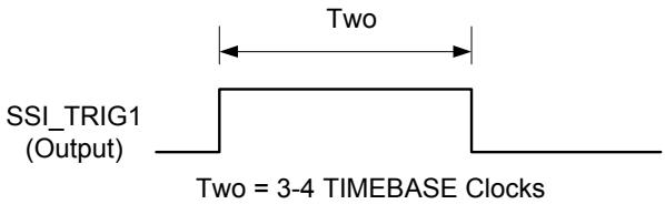
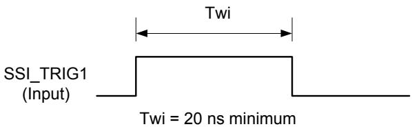
![SST_TRIG1\n(Output)\nTwo\nTwo = 3-4 TIMEBASE Clocks](.pxi-98x6-50-17031-1020-001/1322e479c644e15aa40ed5fcbe208f96e225413b685d8d2c173b12a722ac458d.jpg)

![SSTI_TRIG1\n(Input)\nTwi\nTwi = 20 ns minimum](.pxi-98x6-50-17031-1020-001/9b79fe52856da6d081357e4edd5299c0cb1d2d30419e0448acf39f6545e33ea2.jpg)

Figure 3-21: SSI\_TRIG1 Input and Output Timing Characteristics

# 3.7.3 SSI\_TRIG2 and SSI\_START\_OP

As an output, the SSI\_TRIG2 signal is a clocked SSI\_TRIG1 signal by TIMEBASE, as illustrated in Figure 3-22.
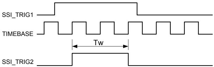
![SSI_TRIG1\nTIMEBASE\nTw\nSSI_TRIG2](.pxi-98x6-50-17031-1020-001/96ba6e7d4e5dacfa0054489b3bfe8058e2614bc4a9fedfb75fcc50da000da830.jpg)

Tw = 2 TIMEBASE Clocks
Figure 3-22: SSI\_TRIG2 Output Timing

As an input, the PCI/PXI-9816/26/46 accepts the SSI\_TRIG2 signal to be the source of a one-clock delayed trigger event. The controller on the PCI/PXI-9816/26/46 will then compensate the oneclock delay if using SSI\_TRIG2 as the source of trigger event. The signal is configured in the rising edge-detection mode.
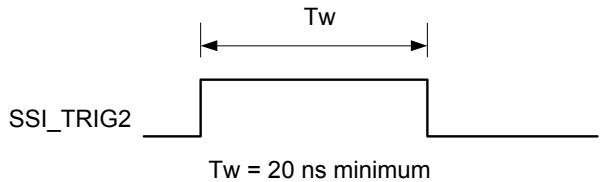
![SST_TRIG2\nTw = 20 ns minimum](.pxi-98x6-50-17031-1020-001/597d75c0ea43df3e527eb7b8e77090bc6d3e0175275ef1a7fd0d7cac833b18fa.jpg)

Figure 3-23: SSI\_TRIG2 Input Timing Requirement

As an output, the SSI\_START\_OP signal reflects the operation start signal in a pre-trigger or middle-trigger acquisition sequence. Please refer to Figure 3-12 - Figure 3-14 for the relationship between the operation start signal and the acquisition sequence.

As an input, the PCI/PXI-9816/26/46 accepts the SSI\_START\_OP signal to be the operation start signal in a pre-trigger or middletrigger acquisition sequence. The signal is configured in the rising edge-detection mode. Figure 3-24 show the SSI\_START\_OP signal input and output timing requirements.

For enabling output operations, you can use the function SSI\_SourceConn() to output the SSI\_TRIG2 and SSI\_START\_OP signals.

For the input operations, you can select TRSRC\_SSI\_2 to set SSI\_TRIG2 and SSI\_START\_OP as the source of the trigger event and operation start signal.
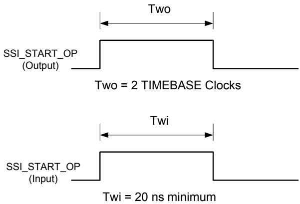
![SST_START_OP\n(Output)\nTwo = 2 TIMEBASE Clocks\nSST_START_OP\n(Input)\nTwi = 20 ns minimum](.pxi-98x6-50-17031-1020-001/cc377ec05e14cf72f58500a7769e609d45bfdb15cfeade9c1eedeff1e58b4ec6.jpg)

Figure 3-24: SSI\_START\_OP Output and Input Timing Characteristics

# 3.7.4 Comparing the Different Trigger Sources from SSI

When selecting TRSRC\_SSI\_1 as the trigger source input, the signal SSI\_TRIG1 reflects the trigger event signal in an acquisition sequence. However, when synchronizing multiple PCI/PXI-9816/ 26/46 devices, each module may recognize the trigger signal with one-clock time difference because the signal is not related to the timebase.

There is another phenomenon if using TRSRC\_SSI\_2 in pre-trigger and middle-trigger mode. The operation start signal is generated by a software command so multiple PCI/PXI-9816/26/46 modules don’t start the data acquisition simultaneously, which may result in the fact that the amount of stored samples are different if the trigger event occurs before the specified amount of data has been acquired.

When selecting TRSRC\_SSI\_2 as the trigger source input, SSI\_TRIG2 and SSI\_START\_OP can achieve better synchronization between multiple PCI/PXI-9816/26/46 devices. A clocked SSI\_TRIG2 can guarantee all PCI/PXI-9816/26/46 devices recognize the trigger event at the same clock edge if they use the same timebase. In pre-trigger and middle-trigger mode, SSI\_START\_OP guarantees all the PCI/PXI-9816/26/46 devices start the data acquisition at the same time.

# 3.8 Physical Location of the PXI and PCI Digitizer

# 3.8.1 Identify PXI Digitizer’s Physical Location by Geographic Address

CompactPCI and PXI chassis accommodate slot numbering mechanism based on the definition of Geographical Address pins on its backplane. Users can identify module’s physical location by reading back Geographical Address. This is a useful feature especially when multiple modules are installed in one host system. The PXI-9816/26/46 can read back the Geographical Address through software driver. Please refer to software function reference manual for more detail description.

# 3.8.2 Assign a Board ID to a PCI Digitizer

When users plug two or more PCI-9816/26/46 modules in one computer, board ID provides an effective mechanism for user to identity the specific module. With this method, users can access to specific module in accordance with board ID. The dip switch of board ID is located on the top of the module. Please refer to following figure and table for detail setting.

Please note that users have to assign a unique board ID to each module that are installed in the same computer, otherwise software driver will not allocate correct system resource to these modules. Once users assign identical board ID to different module, please turn off your computer first and then adjust the board ID again. After correct board ID is assigned, then users can power up computer again.
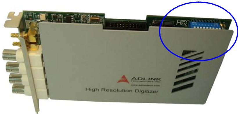
![ADLINK\nTECHNOLOGY & CO.,LTD.\nwww.adlinktech.com\nHigh Resolution Digitizer](.pxi-98x6-50-17031-1020-001/4e1b5593a089974793c314806b384e66e34f6ebb0cd1f084ff10cfc499b6073a.jpg)

Figure 3-25: The Location of Board ID Switch
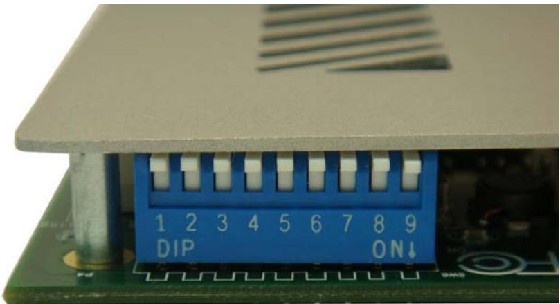
![1 2 3 4 5 6 7 8 9\nDIP ON↓\nfd SMS](.pxi-98x6-50-17031-1020-001/6a2c69dbdf957ebf4b5ef2152c64a9863d2ff14278adf7fb5083a202b1c9b4f9.jpg)

Figure 3-26: Enlargement of Board ID setting.

Note:

Only dip switches 1-5 are valid for board ID settings. Dip switches 6- 9 are unused. When a dip switch is switched to ‘ON’, it represents $" 1 "$ , the opposite direction represents $\mathfrak { v }$ .

1: ON

0: OFF

<table><tr><td rowspan="2">Board ID</td><td colspan="5">Switch Number</td></tr><tr><td>1</td><td>2</td><td>3</td><td>4</td><td>5</td></tr><tr><td>0</td><td>1</td><td>1</td><td>1</td><td>1</td><td>1</td></tr><tr><td>1</td><td>0</td><td>1</td><td>1</td><td>1</td><td>1</td></tr><tr><td>2</td><td>1</td><td>0</td><td>1</td><td>1</td><td>1</td></tr><tr><td>3</td><td>0</td><td>0</td><td>1</td><td>1</td><td>1</td></tr><tr><td>4</td><td>1</td><td>1</td><td>0</td><td>1</td><td>1</td></tr><tr><td>5</td><td>0</td><td>1</td><td>0</td><td>1</td><td>1</td></tr><tr><td>6</td><td>1</td><td>0</td><td>0</td><td>1</td><td>1</td></tr><tr><td>7</td><td>0</td><td>0</td><td>0</td><td>1</td><td>1</td></tr><tr><td>8</td><td>1</td><td>1</td><td>1</td><td>0</td><td>1</td></tr><tr><td>9</td><td>0</td><td>1</td><td>1</td><td>0</td><td>1</td></tr><tr><td>10</td><td>1</td><td>0</td><td>1</td><td>0</td><td>1</td></tr><tr><td>11</td><td>0</td><td>0</td><td>1</td><td>0</td><td>1</td></tr><tr><td>12</td><td>1</td><td>1</td><td>0</td><td>0</td><td>1</td></tr><tr><td>13</td><td>0</td><td>1</td><td>0</td><td>0</td><td>1</td></tr><tr><td>14</td><td>1</td><td>0</td><td>0</td><td>0</td><td>1</td></tr><tr><td>15</td><td>0</td><td>0</td><td>0</td><td>0</td><td>1</td></tr><tr><td>16</td><td>1</td><td>1</td><td>1</td><td>1</td><td>0</td></tr><tr><td>17</td><td>0</td><td>1</td><td>1</td><td>1</td><td>0</td></tr><tr><td>18</td><td>1</td><td>0</td><td>1</td><td>1</td><td>0</td></tr><tr><td>19</td><td>0</td><td>0</td><td>1</td><td>1</td><td>0</td></tr><tr><td>20</td><td>1</td><td>1</td><td>0</td><td>1</td><td>0</td></tr><tr><td>21</td><td>0</td><td>1</td><td>0</td><td>1</td><td>0</td></tr><tr><td>22</td><td>1</td><td>0</td><td>0</td><td>1</td><td>0</td></tr><tr><td>23</td><td>0</td><td>0</td><td>0</td><td>1</td><td>0</td></tr><tr><td>24</td><td>1</td><td>1</td><td>1</td><td>0</td><td>0</td></tr><tr><td>25</td><td>0</td><td>1</td><td>1</td><td>0</td><td>0</td></tr><tr><td>26</td><td>1</td><td>0</td><td>1</td><td>0</td><td>0</td></tr><tr><td>27</td><td>0</td><td>0</td><td>1</td><td>0</td><td>0</td></tr><tr><td>28</td><td>1</td><td>1</td><td>0</td><td>0</td><td>0</td></tr><tr><td>29</td><td>0</td><td>1</td><td>0</td><td>0</td><td>0</td></tr><tr><td>30</td><td>1</td><td>0</td><td>0</td><td>0</td><td>0</td></tr><tr><td>31</td><td>0</td><td>0</td><td>0</td><td>0</td><td>0</td></tr></table>

Table 3-6: Board ID Combination Conditions

# Important Safety Instructions

Please read and follow all instructions marked on the product and in the documentation before operating the system. Retain all safety and operating instructions for future use.

 Please read these safety instructions carefully.
 Please keep this User’s Manual for future reference.
 The equipment should be operated in an ambient temperature between 0 to 50C.
 The equipment should be operated only from the type of power source indicated on the rating label. Make sure the voltage of the power source is correct when connecting the equipment to the power outlet.
If the user’s equipment has a voltage selector switch, make sure that the switch is set to the proper position for the area. The voltage selector switch is set at the factory to the correct voltage.
 For pluggable equipment, ensure they are installed near a socket-outlet that is easily accessible.
 Secure the power cord to prevent unnecessary accidents. Do not place anything over the power cord.
If the equipment will not be in use for long periods of time, disconnect the equipment from mains to avoid being damaged by transient overvoltage.
 All cautions and warnings on the equipment should be noted.
 Please keep this equipment away from humidity.
 Do not use this equipment near water or a heat source.
 Place this equipment on a reliable surface when installing. A drop or fall could cause injury.
 Never pour any liquid into the opening, this could cause fire or electrical shock.

Openings in the case are provided for ventilation. Do not block or cover these openings. Make sure there is adequate space around the system for ventilation when setting up the work area. Never insert objects of any kind into the ventilation openings.
 To avoid electrical shock, always unplug all power and modem cables from the wall outlets before removing covers.
 Lithium Battery provided (real time clock battery)

“CAUTION - Risk of explosion if battery is replaced by an incorrect type. Dispose used batteries as instructed in the instructions”

 The equipment should be checked by service personnel if one of the following situation arises:

 The power cord or plug is damaged.
 Liquid has penetrated the equipment.
 The equipment has been exposed to moisture.
 The equipment is not functioning or does not function according to the user’s manual.
 The equipment has been dropped and damaged.
 If the equipment has obvious sign of breakage.

 Never open the equipment. For safety reasons, the equipment should only be opened by qualified service personnel.
[🔗 Link to the original document](.pxi-98x6-50-17031-1020-001/pxi-98x6-50-17031-1020-001.pdf)
