# PXIe-3988/3987/3977/3937-TL

PXI Express Embedded Controller

User’s Manual

![Exterior view of a ADLINK PXIe 3987-10 PCIe Embedded Controller module (no visible text or symbols on main body)](.pxie-39xx-tl-50m-38008-1000-10/5bfd4cbc1b52d057e8e81a8d4831223f0ee5fcbcd2701213a56ea9e89e49f1c1.jpg)

Manual Rev.: 1.0

Revision Date: Jan. 19, 2026

Part No: 50M-38008-1000

# Revision History

<table><tr><td>Revision</td><td>Release Date</td><td>Description of Change(s)</td></tr><tr><td>1.0</td><td>2026-01-19</td><td>Initial release</td></tr></table>

# Preface

# Copyright © 2026 ADLINK Technology, Inc.

This document contains proprietary information protected by copyright. All rights are reserved. No part of this manual may be reproduced by any mechanical, electronic, or other means in any form without prior written permission of the manufacturer.

# Disclaimer

The information in this document is subject to change without prior notice in order to improve reliability, design, and function and does not represent a commitment on the part of the manufacturer.

In no event will the manufacturer be liable for direct, indirect, special, incidental, or consequential damages arising out of the use or inability to use the product or documentation, even if advised of the possibility of such damages.

ADLINK is committed to fulfill its social responsibility to global environmental preservation through compliance with the European Union's Restriction of Hazardous Substances (RoHS) directive and Waste Electrical and Electronic Equipment (WEEE) directive. Environmental protection is a top priority for ADLINK. We have enforced measures to ensure that our products, manufacturing processes, components, and raw materials have as little impact on the environment as possible. When products are at their end of life, our customers are encouraged to dispose of them in accordance with the product disposal and/or recovery programs prescribed by their nation or company.

![Symbol of a trash bin crossed with a diagonal line and a horizontal bar below (no text or labels)](.pxie-39xx-tl-50m-38008-1000-10/4c4a06ebf26c6d39bda13a9918089accf06a93b27438facb1e04f82ce9bdcd28.jpg)

Battery Labels (for products with battery)
![Symbol of a trash bin crossed out by two diagonal lines (no text or numbers present)](.pxie-39xx-tl-50m-38008-1000-10/62a8d23432e0bed73066084634c95a670ba2e394b669137e4ea9b4f0c74faad6.jpg)

![Recycling symbol icon with three chasing arrows inside a square frame (no text or labels)](.pxie-39xx-tl-50m-38008-1000-10/8c899fb62e7e936c3deaab51c2ed20b3b6f38b013f179cd118f86f1f645fa08b.jpg)

Li-ion

![RECYCLE\nRBRC\nLi-ion\n7.800.822.8837](.pxie-39xx-tl-50m-38008-1000-10/940213cc4cf04d14747a46d6878eddad8fb6aa17829ee6f6535b218b3bdb534e.jpg)

![Abstract geometric pattern with interlocking black and white shapes (no text or symbols)](.pxie-39xx-tl-50m-38008-1000-10/743242b43bf79382e02e78541d789787ccc22f32b2ef6db2168efa294940e750.jpg)

ᘄ㟁ụㄳᅇᨲ

# California Proposition 65 Warning

![A yellow triangle with a thick black border containing a centered black exclamation point.](.pxie-39xx-tl-50m-38008-1000-10/f1b49943c104b3e2f381ed54c41cafe866d283307ed9e554d4a8b111476c8ea4.jpg)

WARNING: This product can expose you to chemicals including acrylamide, arsenic, benzene, cadmium, Tris(1,3-dichloro-2-propyl)phosphate (TDCPP), 1,4-Dioxane, formaldehyde, lead, DEHP, styrene, DINP, BBP, PVC, and vinyl materials, which are known to the State of California to cause cancer, and acrylamide, benzene, cadmium, lead, mercury, phthalates, toluene, DEHP, DIDP, DnHP, DBP, BBP, PVC, and vinyl materials, which are known to the State of California to cause birth defects or other reproductive harm. For more information go to www.P65Warnings.ca.gov.

# Trademarks

Product names mentioned herein are used for identification purposes only and may be trademarks and/or registered trademarks of their respective companies.

# Conventions

Take note of the following conventions used throughout this manual to make sure that users perform certain tasks and instructions properly.

![This is a graphic of a white document icon with a folded top-right corner and faint gray horizontal lines. A large red checkmark is superimposed over the center of the document.](.pxie-39xx-tl-50m-38008-1000-10/d3e0d5fc3345122683d56e0c972c418d38c30c741b48e05b06f38adf1e396e50.jpg)
NOTE:

Additional information, aids, and tips that help users perform tasks.

![The image shows a yellow triangular warning sign with a black border. Inside the triangle is a large black exclamation point. Above the triangle, a horizontal black line is visible, indicating the bottom edge of a rectangular section above the sign.](.pxie-39xx-tl-50m-38008-1000-10/138cb4b7286657bf24421849adb13d948349f74d579bec1360be6dd7e63ed95a.jpg)
CAUTION:

Information to prevent minor physical injury, component damage, data loss, and/or program corruption when trying to complete a task.

![The image displays a standard warning sign featuring a red equilateral triangle with an exclamation point in its center. The triangle is solid red, and the exclamation mark is white. At the very top edge of the image, a thin black horizontal line is visible.](.pxie-39xx-tl-50m-38008-1000-10/6ba91c3e5027659c636281093f549d3cddba03e71da0dd486b69057291385e20.jpg)
WARNING:

Information to prevent serious physical injury, component damage, data loss, and/or program corruption when trying to complete a specific task.

# Table of Contents

# Revision History........ ii

# Preface ............ iii

# List of Figures ....... ix

# List of Tables......... . xi

# 1 Introduction .......

1.1 Features...... 2
1.2 Specifications..... 3
1.3 I/O and Indicators . 7

1.3.1 Front Panel ..
1.3.2 GPIB Connector .. ... 10
1.3.3 Reset Button ..... .. 11
1.3.4 LED Indicators .... .. 11
1.3.5 USB 2.0 Ports .... ... 11
1.3.6 Gigabit Ethernet Ports .... .. 12
1.3.7 USB 3.0 Ports ..... .. 13
1.3.8 COM Port... .. 14
1.3.9 Onboard Connections and Settings.... .. 15

# 2 Getting Started ..... . 17

2.1 Package Contents .... . 17
2.2 Operating System Installation..... 1 8

2.2.1 Installation Environment . . 19
2.2.2 Installing the PXIe-3988/3987/3977/3937-TL ........... 20
2.2.3 Replacing the Hard Drive or Solid State Drive ......... 23
2.2.4 Replacing the Battery Backup ...... .. 25
2.2.5 Clearing CMOS . .. 26

# 3 Driver Installation.......... . 27

# A Appendix: PXI Trigger I/O Function Reference...............29

A.1 Data Types..... 30
A.2 Function Library ..... 31

A.2.1 TRIG\_Init .. ... 31
A.2.2 TRIG\_Close ...... ... 32
A.2.3 TRIG\_SetSoftTrg.. ... 33
A.2.4 TRIG\_Trigger\_Route ..... .. 33
A.2.5 TRIG\_Trigger\_Clear ...... ... 35
A.2.6 TRIG\_GetSoftTrg....... ... 36
A.2.7 TRIG\_Trigger\_Route\_Query ........ ... 36
A.2.8 TRIG\_GetDriverRevision. .. 38

# B Appendix: BIOS Setup.......... ....41

B.1 Menu Structure .. . 41
B.2 Starting the BIOS .... 42
B.3 Main .. . 44

B.3.1 BIOS Information ... .. 44
B.3.2 System Information..... .. 44
B.3.3 System Management.. .. 45

B.4 Advanced... 48

B.4.1 CPU Configuration..... .. 48
B.4.2 Memory Configuration .. . 49
B.4.3 Graphics Configuration.. . 49
B.4.4 Onboard Devices Configuration.. .. 50
B.4.5 USB Configuration ..... .. 51
B.4.6 Network Stack Configuration .... . 51
B.4.7 Advanced Power Management . . 52
B.4.8 Hardware Health Configuration .. . 52
B.4.9 PXIe Links Control Configuration.. .. 52

B.5 Boot .. 53

B.5.1 Boot Configuration.. ... 53

B.5.2 CSM Configuration .... .. 54

B.6 Security ..... 5 5

B.6.1 Password Description.. . 55

B.7 Save & Exit ... 5 6

# C Appendix: Dual BIOS ...... .. 57

# Important Safety Instructions ...... 59

# Getting Service......... . 61

This page intentionally left blank.

# List of Figures

Figure 1-1: Functional Block Diagram.. . 3

Figure 1-2: Front Panel ..

Figure 1-3: PXI Trigger SMB Jack . . 8

Figure 1-4: DisplayPort Connector.. . 9

Figure 1-5: GPIB Connector.. . 10

Figure 1-6: LED Indicators . . 11

Figure 1-7: COM Port... . 14

Figure 1-8: Onboard Configuration .. . 15

Figure B-1: BIOS Setup Navigation... .. 43

This page intentionally left blank.

# List of Tables

Table 1-1: Front Panel Legend .

Table 1-2: DisplayPort Pin Assignment . . 9

Table 1-3: GPIB Pin Description ... . 10

Table 1-4: LED Indicator Legend. . 11

Table 1-5: USB 2.0 Port Pin Assignment.. . 12

Table 1-6: Ethernet Port Pin Assignments. . 12

Table 1-7: D-sub COM Port Signal Functions... . 14

Table 1-8: Onboard Configuration Legend . . 15

Table B-1: BIOS Hot Key Functions... .. 43

This page intentionally left blank.

# 1 Introduction

The ADLINK PXIe-3988/3987/3977/3937-TL PXI Express™ embedded controller is based on the twelfth generation Intel® Core™ i7/i5/i3 processor specifically designed for PXI Expressbased testing systems. A rugged and stable operating environment is provided for a variety of testing and measurement applications.

Combining state-of-the-art Intel® Xeon® W-11865MRE/Core™i7- 11850HE/i5-11500HE/i3-11100HE processors and DDR4 3200MHz memory, the PXIe-3988/3987/3977/3937-TL utilizes separate computing engines on a single processor, enabling execution of multiple independent tasks simultaneously. With a configurable PCIe switch, the PXIe-3988/3987/3977/3937-TL can support four links at x4 or two links at x8 x16 PXI Express link capability, with maximum system throughput of up to 16GB/s (PCI Express 3.0).

PXI Express-based testing systems typically make up a PXI Express platform and diversified standalone instruments for complex testing tasks. The PXIe-3988/3987/3977/3937-TL series provides ample interfaces, including two DisplayPort connectors, allowing connection to two monitors, dual USB 3.0 connections for high speed peripheral devices, dual Gigabit Ethernet ports, one for LAN connection and the other for controlling LXI instruments, four USB 2.0 ports for peripheral devices and USB instrument control, and a Micro-D GPIB connector for GPIB instrument connection, allowing for control of hybrid PXI-based testing systems.

![The image displays a white document icon featuring faint horizontal lines and a folded top-left corner. A large, red checkmark is drawn over the left side of the document.](.pxie-39xx-tl-50m-38008-1000-10/78b396122438cdca7f949e53a6963310e0561374bc53ec3d9c683f472a295160.jpg)
NOTE:

Memory addressing over 4GB is OS-dependent, such that a 32-bit operating system may be unable to address memory space over 4GB. To fully utilize memory, 64-bit operating systems are required.

# 1.1 Features

 PXITM-5 PXI Express Hardware Specification Rev.1.1
Intel® Xeon® W-11865MRE/Core™i7-11850HE/i5-11500HE/ i3-11100HE processor for maximum computing power
 DDR4 SODIMM x2
 Default: 16G, up to 32G 3200MHz
 Maximum System Throughput 16GB/s
 PXI Express Link Capability
 Four Link Configuration: x4 x4 x4 x4
 Two Link Configuration: x8 x16
 Optional SATA SSD
 Supports 2.5” SSD
 SATA 6.0 Gb/s
 Supports AHCI
 Integrated I/O
 Dual Gigabit Ethernet ports
 Two USB 3.0 Ports
 Four USB 2.0 Ports
 Built-in GPIB (IEEE488) controller
 Dual DisplayPort connectors
 One COM port (D-sub 9-pin serial)
 Trigger I/O for advanced PXITM trigger functions

 Microsoft Windows 10/11 64-bit

# 1.2 Specifications

![Based on the provided flowchart/block diagram, here are the labeled blocks and their connections:\n\n**1. Front Panel Connectors (Left Column)**\n*   **DisplayPort Connector x2**: Connected to the processor via **DP/HDMI Dual Mode**.\n*   **GPIB Connector**: Connected to a **GPIB Controller**.\n*   **GbE Connector** (Two instances): Each connected to an **Ethernet Controller**.\n*   **USB3.0 Connector x2**: Connected to the chipset via **USB 3.0**.\n*   **USB2.0 Connector x4**: Connected to the chipset via **USB 2.0**.\n*   **COM Port Connector (RS-232/422/485)**: Connected to an **LPC-COM Port**.\n*   **SMB Connector**: Connected to the **SMBus Controller / Programmable MUX** via **Trigger Signal**.\n\n**2. Processor and Chipset (Center)**\n*   **Mobile Intel 11th Gen Intel Xeon / Core i7/i5/i3 Processor (formerly 'Tiger Lake')**:\n    *   Connected to **DDR4 3200 MHz SODIMM** via **Memory Bus** and **PCIe 3.0 x16**.\n    *   Connected to **PCI Express Switch (PCI Express 3.0)** via **PCIe 3.0 x16**.\n    *   Connected to the **Mobile Intel QM580E Chipset** via **DMI 3.0**.\n*   **Mobile Intel QM580E Chipset**:\n    *   Connected to the **GPIB Controller** and two **Ethernet Controller** blocks.\n    *   Connected to the **LPC-COM Port** via **LPC**.\n    *   Connected to **BGA SSD** via **NVMe**.\n    *   Connected to the **SMBus Controller / Programmable MUX** via **PCIe x1**.\n\n**3. Peripheral Controllers (Between Left and Center)**\n*   **GPIB Controller**: Connects the GPIB Connector to the Chipset.\n*   **Ethernet Controller** (Two instances): Connect the GbE Connectors to the Chipset.\n*   **LPC-COM Port**: Connects the COM Port to the Chipset via **LPC**.\n*   **BGA SSD**: Connected to the Chipset via **NVMe**.\n*   **SMBus Controller / Programmable MUX**: Connected to the Chipset via **PCIe x1**.\n\n**4. Expansion and Memory (Right Side)**\n*   **DDR4 3200 MHz SODIMM**: Connected to the Processor via **Memory Bus** and **PCIe 3.0 x16**.\n*   **PCI Express Switch (PCI Express 3.0)**: Connected to the Rear Connectors via **PCIe 3.0 2 Link Mode (x16 x8) OR PCIe 3.0 4 Link Mode (x4 x4 x4 x4)**.\n*   **Rear Connectors to PXI Express Chassis**: Connected to the PCI Express Switch via the PCIe modes listed above. Connected to the **SMBus Controller / Programmable MUX** via **SMBus** and **Trigger Bus**.](.pxie-39xx-tl-50m-38008-1000-10/87757445af93b564e53a9d380bd93160ce81cdba13d03b43f972ac37b8893d87.jpg)

Figure 1-1: Functional Block Diagram

# Processor

Intel® Xeon® W-11865MRE/Core™i7-11850HE/i5-11500HE/ i3-11100HE processor

# Memory

 Two standard 260-pin DDR4 SODIMM sockets
 Supports 3200MHz RAM up to 32GB total
 Supports non-ECC, unbuffered memory

![The image displays a simple icon of a white document or piece of paper with a folded top-right corner and faint horizontal lines running across the bottom half. Superimposed over the document is a large, bold red checkmark (or tick) that spans diagonally from the bottom left to the upper right.](.pxie-39xx-tl-50m-38008-1000-10/f7163faca138ffe5e66a56e3adea04dfa5d59cd5d1fe9c545747901317179241.jpg)
NOTE:

The externally accessible SODIMM socket can accept replacement DDR4 DRAM DIMM modules.

PXIe-3988/3987/3977/3937-TL specifications and stability guarantees are only supported when ADLINK-provided DDR4 DRAM SODIMM modules are used.

# Video

 DisplayPort supports up to 3840 x 2160 @ 60Hz resolution
 DVI (with passive DisplayPort-to-DVI adapter) supports resolution up to 1920 x 1200 @ 60 Hz

![The image displays a white document icon featuring horizontal grey lines, resembling a piece of paper or a checklist. The top right corner of the paper is folded down. A large, red checkmark is superimposed diagonally across the left side of the document.](.pxie-39xx-tl-50m-38008-1000-10/223c1b5284bfaefdc68f280c25b4c31561faed5747326fe2b9c90ad8adfde24b.jpg)
NOTE:

DisplayPort adapters for other standards are available, with maximum available resolution dependent on the adapter chosen

# Storage

Built-in 512GB NVMe SSD and optional SATA port for 2.5" SSD.

# I/O Connectivity

Dual Gigabit Ethernet controllers through two RJ45 connectors with speed/link/active LED on the faceplate.

# USB

Four USB 2.0 and two USB 3.0 ports on the faceplate.

# GPIB

Onboard IEEE488 GPIB controller through Micro-D 25-pin connector on the faceplate.

# Trigger I/O

One SMB connector on the faceplate to route an external trigger signal to/from PXI trigger bus

# Dimensions (3U PXI module)

3U/4-slot PXI standard

# Weight

1.0 kg (exclusive of packaging)

# Environmental

<table><tr><td>Operating temperature with SSD</td><td>0 to 55°C</td></tr><tr><td>Storage temperature</td><td>-40 to 71°C</td></tr><tr><td>Relative humidity, non-condensing</td><td>5 to 95%</td></tr></table>

# Shock and Vibration

Functional shock 30G, half-sine, 11ms pulse duration

Random vibration:

 Operating 5 to 500Hz, 0.21Grms, 3 axes
 Non-operating 5 to 500Hz, 2.46Grms, 3 axes

![The image displays an icon of a white piece of paper with a folded top-right corner and faint blue horizontal lines. A large, thick red checkmark is drawn diagonally across the front of the paper.](.pxie-39xx-tl-50m-38008-1000-10/e0b9693a796ad4fbea640c4d60bfda3ca37f18122f481c480c65ce18048725cf.jpg)
NOTE:

Environmental & Shock and Vibration values are only guaranteed with use of an ADLINK-provided SSD.

# Certification

Electromagnetic compatibility:

EN 61326-1 (IEC 61326-1): Class A emissions; Basic immunity
 EN 55011 (CISPR 11): Group 1, Class A emissions
 EN 55032 2015/AC: 2016 Class A
 EN 55032 2015/AC: 2016 Class B
 EN 55024 2010+ A1: 2015
 EN 61000-3-2:2014: Class A
 EN 61000-3-3:2013: Class A
 EN 55024:2010+A1:2015: Immunity
 FCC 47 CFR Part 15 Subpart A (Class A)
 FCC 47 CFR Part 15 Subpart B (Class B)
 ICES-001 Class A
 ICES-003 Issue 6-2016
 AS/NZS CISPR 11: Group 1, Class A emissions
 AS/NZS CISPR 32: 2015 (Ed 2.0)/C1:2016 : Class B

The PXIe-3988/3987/3977/3937-TL meets the essential requirements of applicable European Directives.

Power Requirements

<table><tr><td>Typical Consumption</td><td>DC +3.3V</td><td>DC +5V</td><td>DC +12V</td></tr><tr><td>Typical operation(Measured while W10 is idle)</td><td>1.722A</td><td>5.687A</td><td>1.953A</td></tr><tr><td>Heavy operation(Measured while W10 is under heavy CPU and storage utilization)</td><td>1.728A</td><td>6.460A</td><td>6.000A</td></tr></table>

# 1.3 I/O and Indicators

# 1.3.1 Front Panel

![ADLINK\nHD USR\nPW\nA\nH\nTGIC\nB\nG\nC\nD\nF\nGPIB\nCOM\nE\nPXIe-3987-71\nPXIe Embedded Controller](.pxie-39xx-tl-50m-38008-1000-10/694cfb1004035fefb73d76c1551530e0c3014f91425f0e9c854be3ec2cac00fa.jpg)

Figure 1-2: Front Panel

<table><tr><td>A</td><td>Reset Button</td><td>F</td><td>GPIB Connector(Micro D-sub 25-pin)</td></tr><tr><td>B</td><td>2x DisplayPort</td><td>G</td><td>2x Gigabit Ethernet</td></tr><tr><td>C</td><td>2x USB 3.0</td><td>H</td><td>PXI Trigger</td></tr><tr><td>D</td><td>4x Type-A USB 2.0</td><td rowspan="2">I</td><td rowspan="2">LED indicators</td></tr><tr><td>E</td><td>COM port(D-sub 9-pin serial)</td></tr></table>

Table 1-1: Front Panel Legend

# PXI Trigger Connector

![Ground\nTrigger](.pxie-39xx-tl-50m-38008-1000-10/947d5ab321dfaf594639b474f5807405fa32ed1df3e728b4d7d249ec8969a585.jpg)

Figure 1-3: PXI Trigger SMB Jack

The PXI trigger connector is an SMB jack, used to route external trigger signals to or from the PXI backplane. Trigger signals are TTL-compatible and edge sensitive. The PXIe-3988/3987/3977/ 3937-TL provides four trigger routing modes from/to the PXI trigger connector to synchronize PXI modules, including

 From a selected trigger bus line to PXI trigger connector
 From the PXI trigger connector to a selected trigger bus line
 From software trigger to a selected trigger bus line
 From software trigger to PXI trigger connector

All trigger modes are programmable by the provided driver.

# DisplayPort Connectors

Provides monitor connection for VGA/DVI/HDMI monitors; installation of requisite adapters required. Dual display function is also supported.

![19\n1\n20\n2](.pxie-39xx-tl-50m-38008-1000-10/3d194de803804aae3b1246648c04091d340d819842de62fbf9b02e309ba6bbb6.jpg)

Figure 1-4: DisplayPort Connector

<table><tr><td>Pin</td><td>Signal</td><td>Pin</td><td>Signal</td></tr><tr><td>1</td><td>CN_DDPx0+</td><td>11</td><td>GND</td></tr><tr><td>2</td><td>GND</td><td>12</td><td>CN_DDPx3-</td></tr><tr><td>3</td><td>CN_DDPx0-</td><td>13</td><td>CN_DDPx_AUX_SEL</td></tr><tr><td>4</td><td>CN_DDPx1+</td><td>14</td><td>CN_DDPx_CONFIG2</td></tr><tr><td>5</td><td>GND</td><td>15</td><td>CN_DDPx_AUX+</td></tr><tr><td>6</td><td>CN_DDPx1-</td><td>16</td><td>GND</td></tr><tr><td>7</td><td>CN_DDPx2+</td><td>17</td><td>CN_DDPx_AUX-</td></tr><tr><td>8</td><td>GND</td><td>18</td><td>CN_DDPx_HPD</td></tr><tr><td>9</td><td>CN_DDPx2-</td><td>19</td><td>GND</td></tr><tr><td>10</td><td>CN_DDPx3+</td><td>20</td><td>+V3.3_DDPx_PWR</td></tr></table>

Table 1-2: DisplayPort Pin Assignment

# 1.3.2 GPIB Connector

The GPIB connector on PXIe-3988/3987/3977/3937-TL is a micro Dsub 25-pin connector, controlling external bench-top instruments. Connection to other instruments requires the optional ACL-IEEE488- MD1-A cable. The onboard GPIB controller provides:

 Full compatibility with IEEE 488 standard
 Up to 1.5MB/s data transfer rates
 Onboard 2KB FIFO for read/write operations
 Driver APIs are compatible with NI-488.2 driver software
 Connection for up to 14 instruments

![1\n13\n14\n25](.pxie-39xx-tl-50m-38008-1000-10/434d5ff57b54a214a3f9465830a3a6fe7c47294a5cbdb5ba44b56258f7fb3ee7.jpg)

Figure 1-5: GPIB Connector

<table><tr><td>Pin</td><td>Signal</td><td>Description</td><td>Pin</td><td>Signal</td><td>Description</td></tr><tr><td>1</td><td>DIO1#</td><td>GPIB Data 1</td><td>14</td><td>DIO5#</td><td>GPIB Data 5</td></tr><tr><td>2</td><td>DIO2#</td><td>GPIB Data 2</td><td>15</td><td>DIO6#</td><td>GPIB Data 6</td></tr><tr><td>3</td><td>DIO3#</td><td>GPIB Data 3</td><td>16</td><td>DIO7#</td><td>GPIB Data 7</td></tr><tr><td>4</td><td>DIO4#</td><td>GPIB Data 4</td><td>17</td><td>DIO8#</td><td>GPIB Data 8</td></tr><tr><td>5</td><td>EOI</td><td>End Or Identify</td><td>18</td><td>REN</td><td>Remote Enable</td></tr><tr><td>6</td><td>DAV</td><td>Data Valid</td><td>19</td><td>Ground</td><td>Signal Ground</td></tr><tr><td>7</td><td>NRFD</td><td>Not Ready For Data</td><td>20</td><td>Ground</td><td>Signal Ground</td></tr><tr><td>8</td><td>NDAC</td><td>No Data Accepted</td><td>21</td><td>Ground</td><td>Signal Ground</td></tr><tr><td>9</td><td>IFC</td><td>Interface Clear</td><td>22</td><td>Ground</td><td>Signal Ground</td></tr><tr><td>10</td><td>SRQ</td><td>Service Request</td><td>23</td><td>Ground</td><td>Signal Ground</td></tr><tr><td>11</td><td>ATN</td><td>Attention</td><td>24</td><td>Ground</td><td>Signal Ground</td></tr><tr><td>12</td><td>Chassis Ground</td><td>Chassis Ground</td><td>25</td><td>Ground</td><td>Signal Ground</td></tr><tr><td>13</td><td>Ground</td><td>Signal Ground</td><td></td><td></td><td></td></tr></table>

Table 1-3: GPIB Pin Description

# 1.3.3 Reset Button

The reset button, activated by insertion of any pin-like implement, executes a hard reset for the PXIe-3988/3987/3977/3937-TL.

# 1.3.4 LED Indicators

Three LED indicators on the faceplate indicate operational status of the PXIe-3988/3987/3977/3937-TL, as follows.

![The image displays the text 'HD USR' in large, black-outlined, uppercase letters on a white background.](.pxie-39xx-tl-50m-38008-1000-10/b1c7f476db00ff626bdf9e6e45290200b0899a10a6b70f4633e6ff53d9605e0d.jpg)

![A yellow circle with a thick black outline on a white background.](.pxie-39xx-tl-50m-38008-1000-10/e233679412286c0c4c9083e41e032ea9f708e89efe3b686b4e678073beb79969.jpg)

![The image displays a simple, black outline of a circle on a white background. The line work is thick and slightly uneven, resembling a hand-drawn sketch. There is no text present.](.pxie-39xx-tl-50m-38008-1000-10/5bf00942120a5db898c151081adaf37187c66a9f93fd685e05bf5fede96cf6c8.jpg)

![This image features the capital letters 'PW' in a large, bold, black sans-serif font. The letters are outlined with a thick white stroke.](.pxie-39xx-tl-50m-38008-1000-10/f7ad856e1e8ccc00e9558a096bfba9029998da38c9bc31595233a9b64bf6067f.jpg)

![The image displays two circles positioned side-by-side. On the left is a white circle with a thick black outline. On the right is a solid light green circle.](.pxie-39xx-tl-50m-38008-1000-10/5cddc2225e3fdff6a58fd61ce176ffb70463e7fc597acd29cb6df9c34eba820e.jpg)
Figure 1-6: LED Indicators

<table><tr><td>LED</td><td>Color</td><td>Description</td></tr><tr><td>PW</td><td>Green</td><td>Indicates system power, remaining lit when the system boots normally and main power supply is functioning.</td></tr><tr><td>HD</td><td>Yellow</td><td>Indicates operating state of the HDD or SSD, flashing during access to or activity on the SATA HDD.</td></tr><tr><td>USR</td><td>Blue</td><td>User-programmable LED indicator.</td></tr></table>

Table 1-4: LED Indicator Legend

# 1.3.5 USB 2.0 Ports

The PXIe-3988/3987/3977/3937-TL provides four USB 2.0 ports via USB Type-A connectors on the faceplate, all compatible with hi-speed, full-speed and low-speed USB devices. Supported boot devices include USB flash drive, USB floppy, USB CD-ROM, and others, with boot priority and device settings configurable in the

BIOS. Please see Section B.5.1: Boot Configuration for more information.

![Pure electrical connector pinout diagram without any text or symbols](.pxie-39xx-tl-50m-38008-1000-10/60f2deea6aacd7237942b98ed0e89d1a8b2752c0d3d5fd00ac01c61501b42e6c.jpg)

![1\n2\n3\n4](.pxie-39xx-tl-50m-38008-1000-10/dcf81390223343398826b500eb7fbc5e202c070fef0ba2c18119c0723f7b1e6a.jpg)

<table><tr><td>Pin</td><td>Signal</td></tr><tr><td>1/5</td><td>Power 5V</td></tr><tr><td>2/6</td><td>USB Data-</td></tr><tr><td>3/7</td><td>USB Data +</td></tr><tr><td>4/8</td><td>Ground</td></tr></table>

Table 1-5: USB 2.0 Port Pin Assignment

# 1.3.6 Gigabit Ethernet Ports

Dual Gigabit Ethernet connection is provided on the PXIe-3988/ 3987/3977/3937-TL front panel.

<table><tr><td>Pin</td><td>1000Base-T Signal</td><td>100/10Base-T Signal</td></tr><tr><td>1</td><td>MDI0+</td><td>TX+</td></tr><tr><td>2</td><td>MDI0-</td><td>TX-</td></tr><tr><td>3</td><td>MDI1+</td><td>RX+</td></tr><tr><td>4</td><td>MDI2+</td><td>Reserved</td></tr><tr><td>5</td><td>MDI2-</td><td>Reserved</td></tr><tr><td>6</td><td>MDI1-</td><td>RX-</td></tr><tr><td>7</td><td>MDI3+</td><td>Reserved</td></tr><tr><td>8</td><td>MDI3-</td><td>Reserved</td></tr></table>

Table 1-6: Ethernet Port Pin Assignments

The Ethernet ports each include two LED indicators, one Active/ Link indicator and one Speed indicator, functioning as follows.

<table><tr><td></td><td>LED</td><td>Status</td><td>Description</td></tr><tr><td rowspan="3">&lt;img src="images/3d7ee44d1f0b5d3d626c3ea543c29ea180c94de400bbc43941dbc4cec343560b.jpg"/&gt;</td><td rowspan="3">Active/Link (Yellow)</td><td>Off</td><td>Ethernet port is disconnected</td></tr><tr><td>On</td><td>Ethernet port is connected with no data transmission</td></tr><tr><td>Flashing</td><td>Ethernet port is connected with data transmitted/received</td></tr><tr><td rowspan="3">&lt;img src="images/78092622a3afadb169e630324295cb79638fa2d4febe3f4fb0d9fc099362dac6.jpg"/&gt;</td><td rowspan="3">Speed (Green/Orange)</td><td>Off</td><td>10 Mbps</td></tr><tr><td>Green</td><td>PXle-3988TL: 100 Mbps, 1000 MbpsPXle-3987/3977/3937TL: 100 Mbps</td></tr><tr><td>Orange</td><td>PXle-3988TL: 2.5 GbpsPXle-3987/3977/3937TL: 2.5 Gbps, 1000 Mbps</td></tr></table>

# 1.3.7 USB 3.0 Ports

The PXIe-3988/3987/3977/3937-TL provides two Type-A USB 3.0 ports on the front panel, supporting SuperSpeed, Hi-Speed, fullspeed, and low-speed transmission for downstream. Multiple boot devices, including USB flash, USB external HD, and USB CD-ROM drives are supported, with boot priority configured in BIOS.

![The image features a white document icon with a black outline. Faint gray horizontal lines run across the page. A large, bold red checkmark is drawn over the document.](.pxie-39xx-tl-50m-38008-1000-10/0d072d248b4e772684b2ea13a1d3b06afdca47f9dcee7ccaa82e0e19b3a0d4d0.jpg)
NOTE:

USB 3.0 may not be supported by the OS installation programs/environment. Use USB 2.0 ports for OS installation if necessary.

# 1.3.8 COM Port

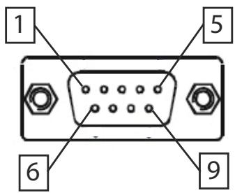
A COM port on the front panel with a D-sub 9-pin connector supports RS-232/RS-422/RS-485 by BIOS selection.
![1\n5\n6\n9](.pxie-39xx-tl-50m-38008-1000-10/ac6d25cb4ee87533f2fde882166de2af26b3d5371770d67ae56a922471c8a09d.jpg)

Figure 1-7: COM Port

<table><tr><td rowspan="2">Pin</td><td colspan="3">Signal Name</td></tr><tr><td>RS-232</td><td>RS-422</td><td>RS-485</td></tr><tr><td>1</td><td>DCD#</td><td>TXD422-</td><td>485DATA-</td></tr><tr><td>2</td><td>RXD</td><td>TXD422+</td><td>485DATA+</td></tr><tr><td>3</td><td>TXD</td><td>RXD422+</td><td>N/S</td></tr><tr><td>4</td><td>DTR#</td><td>RXD422-</td><td>N/S</td></tr><tr><td>5</td><td>GND</td><td>N/S</td><td>N/S</td></tr><tr><td>6</td><td>DSR#</td><td>N/S</td><td>N/S</td></tr><tr><td>7</td><td>RTS#</td><td>N/S</td><td>N/S</td></tr><tr><td>8</td><td>CTS#</td><td>N/S</td><td>N/S</td></tr><tr><td>9</td><td>RI#</td><td>N/S</td><td>N/S</td></tr></table>

Table 1-7: D-sub COM Port Signal Functions

# 1.3.9 Onboard Connections and Settings

![ADLINK\nTECHNOLOGY INC.\nWD Blue®\n500GB\nA\nB\nC\nA\nB\nC\n0.47µH\n1734NC\nR108\nR27\nR528\nSW16\nTC9\nR51\nR521\nClearNormal\nA\nB\nC](.pxie-39xx-tl-50m-38008-1000-10/ee302311100d5c241108c43a5d0d02a78264afdd383d66439393517ce55c566a.jpg)

Figure 1-8: Onboard Configuration

<table><tr><td>A</td><td>Clear CMOS switch</td></tr><tr><td>B</td><td>SATA connector</td></tr><tr><td>C</td><td>System battery</td></tr></table>

Table 1-8: Onboard Configuration Legend

This page intentionally left blank.

# 2 Getting Started

This chapter describes procedures for installing the PXIe-3988/ 3987/3977/3937-TL and making preparations for its operation, including hardware and software setup. Please note that the PXIe-3988/3987/3977/3937-TL is shipped with RAM and onboard SSD preinstalled. Please contact ADLINK or authorized dealer if there are any problems during the installation.

![The image displays a simple graphic icon representing a document or checklist. It features a white sheet of paper with the top-right corner folded down. A large, bold red checkmark is superimposed over the center of the paper. Faint, light gray horizontal lines run across the document, suggesting a list or lines of text.](.pxie-39xx-tl-50m-38008-1000-10/09a6065a73de3cc5c958794ebc2a90638cc3da6ab924fc055ae954a41ce083cc.jpg)
NOTE:

Diagrams and illustrated equipment are for reference only. Actual system configuration and specifications may vary.

# 2.1 Package Contents

Before beginning, check the package contents for any damage and ensure that the following items are included:

 PXIe-3988/3987/3977/3937-TL Controller (equipped with RAM and onboard SSD)
 PXIe-3988/3987/3977/3937-TL Quick Start Guide

If any of these items are missing or damaged, contact the dealer from whom you purchased the product. Save the shipping materials and carton in case you want to ship or store the product in the future.

![The image displays a standard warning symbol consisting of a red equilateral triangle with a black border. Inside the triangle, centered, is a white exclamation point.](.pxie-39xx-tl-50m-38008-1000-10/43a5a1ff20797a10b4c51be1c28817f09a5d5e8df9f594901450d140e4c0bf97.jpg)
WARNING:

Do not install or apply power to equipment that is damaged or missing components. Retain the shipping carton and packing materials for inspection. Please contact your ADLINK dealer/ vendor immediately for assistance and obtain authorization before returning any product.

# 2.2 Operating System Installation

For more detailed information about the operating system, refer to the documentation provided by the operating system manufacturer. Preferred/supported operating systems for PXIe-3988/3987/ 3977/3937-TL are:

 Windows 10/11 64-bit
 For other OS support, please contact ADLINK

Most operating systems require initial installation from a hard drive, floppy drive, or CD-ROM drive. The PXIe-3988/3987/3977/ 3937-TL controller supports USB CD-ROM drive, USB flash disk, USB external hard drive, or a USB floppy drive as the first boot device. Please see Section B.5.1: Boot Configuration for information about setting the boot devices. These devices should be configured, installed, and tested with the supplied drivers before attempting to load the new operating system.

![The image shows a white icon of a document or piece of paper featuring faint horizontal lines. A large, bold red checkmark is superimposed over the center of the page. The top right corner of the paper is folded down in a 'dog-ear' style.](.pxie-39xx-tl-50m-38008-1000-10/9979e2bff609d4c5727c7a2fae050937b621f4a7ea625b1cb2a0c35b3261ca0c.jpg)
NOTE:

Read the release notes and installation documentation provided by the operating system vendor. Be sure to read all the README files or documents provided on the distribution disks, as these typically note documentation discrepancies or compatibility problems.

1. Select the appropriate boot device order from the BIOS Boot Setup Menu based on the OS installation media used. For example, if the OS is distributed on a bootable installation CD, select USB CD-ROM as the first boot device and reboot the system with the installation CD in the USB CD-ROM drive
2. Proceed with the OS installation as directed and be sure to select appropriate device types if prompted. Refer to the appropriate hardware manuals for specific device types and compatibility modes of ADLINK PXI products.
3. When installation is complete, reboot the system and set the boot device order in the SETUP boot menu accordingly.

# 2.2.1 Installation Environment

When preparing to install any equipment described in this manual, please refer to Important Safety Instructions.

Only install equipment in well lit areas on flat, sturdy surfaces with access to basic tools such as flat- and cross-head screwdrivers, preferably with magnetic heads as screws and standoffs are small and easily misplaced.

Recommended Installation Tools include:

 Phillips (cross-head) screwdriver
 Flat-head screwdriver
 Anti-static wrist strap
 Anti-static mat

ADLINK PXIe-3988/3987/3977/3937-TL system controllers are electrostatically sensitive and can be easily damaged by static electricity. The equipment must be handled on a grounded antistatic mat, and operators must wear an anti-static wristband, grounded at the same point as the anti-static mat.

Inspect the carton and packaging for damage. Shipping and handling may cause damage to the contents. Ensure that all contents are undamaged before installing.

![A yellow triangular warning sign features a black exclamation point in the center. Below the triangle, the text 'CAUTION:' is printed in black capital letters.](.pxie-39xx-tl-50m-38008-1000-10/ad8fa32a80fa26559dc4fafd27c0c21c2120fc8ccc46f38a71f666f830c6e521.jpg)

All equipment must be protected from static discharge and physical shock. Never remove any of the socketed parts except at a static-free workstation. Use the antistatic bag shipped with the product to handle the equipment and wear a grounded wrist strap when servicing or installing.

# 2.2.2 Installing the PXIe-3988/3987/3977/3937-TL

1. Remove all screw caps (x4).

![The image displays a four-panel comparison showing a hardware modification involving an electronic device's internal chassis.\n\n**Top Row:**\n*   **Left:** A close-up of a metal chassis corner next to a green circuit board featuring the text 'CE'. Two red circles highlight black plastic mounting posts or pins.\n*   **Right:** The same angle, where the black plastic posts have been replaced by threaded metal screws, which are now highlighted by the red circles.\n*   A large red arrow points from the left image to the right image.\n\n**Bottom Row:**\n*   **Left:** A wider view of the device's interior, showing capacitors and other components. Two red circles highlight black plastic mounting posts at the top and bottom of the chassis frame.\n*   **Right:** The same angle, showing that the black plastic posts have been replaced by threaded metal screws, highlighted by the red circles.\n*   A large red arrow points from the left image to the right image.](.pxie-39xx-tl-50m-38008-1000-10/2f12cde793b54501c822aae6ec106526fb6dc646b6b245e566dca478f5b10d07.jpg)

2. Release the red locking lever.

![Close-up of a black mechanical component with red and black parts, showing a red arrow pointing to a specific area (no text or symbols visible)](.pxie-39xx-tl-50m-38008-1000-10/49ba61af15fd5c02d9f2bacc2e41e4a555dbad2d1d051f7c83c9557059a0dffa.jpg)

3. Depress the latch.

![Close-up of a mechanical device with a red arrow pointing to a red component, no visible text or symbols.](.pxie-39xx-tl-50m-38008-1000-10/ec8f4c23a31899b146ab778edcf1ffe13a32710d658d325acd71db88b1611ee4.jpg)

4. Locate the system controller slot on the chassis (Slot 1).

![ADLINK\n1\n2 H\n3 H\n4 H](.pxie-39xx-tl-50m-38008-1000-10/6331e58c97808d0d2c336d928dede2fb74646bdf0586b47179a9617494f960b7.jpg)

5. Align the controller’s top and bottom edges with the card guides and carefully slide the PXIe-3988/3987/3977/ 3937-TL into the chassis, as shown

![ADLINK\n2 H 3 H 4 H\nADLINK\n01000000000000000000000000000000000000000000000000000000000000000000000000000000000000000](.pxie-39xx-tl-50m-38008-1000-10/d5eaabc70165e54b6703741e58be43ba306af16490b23d7a7d449ad24c09ca17.jpg)

![Close-up of a computer motherboard with a red circle highlighting a component, no visible text or symbols](.pxie-39xx-tl-50m-38008-1000-10/aa6265e2ed377fe7bbce5536ccc1333cd83a31f996dcb6442892137ba0e9ed2b.jpg)

6. Elevate the latch until the PXIe-3988/3987/3977/3937- TL is fully seated in the chassis backplane. The alignment pin on the rear of the latch can be threaded into the best fit alignment port in the chassis rail.

7. Fasten the four mounting screws on the faceplate and connect all peripheral devices.

# 2.2.3 Replacing the Hard Drive or Solid State Drive

The PXIe-3988/3987/3977/3937-TL provides a SATA 3.0 port for optional SSD. Installing an SSD is accomplished as follows.

1. Locate the five screws attaching the hard drive housing to the PXIe-3988/3987/3977/3937-TL controller, as shown.

![WD\nWD50000LPXC\n500GB\nSIN: 3670/1948/1949\nAdvanced Format Drive, 5x seconds hit performance:\n200 GB / 500 GB / 500 GB / 500 GB / 500 GB / 500 GB / 500 GB / 500 GB / 500 GB / 500 GB / 500 GB / 500 GB / 500 GB / 500 GB / 500 GB / 500 GB / 500 GB / 500 GB\nWDS: WD50000LPXC - 420V/420\nWDS: WD50000LPXC - 420V/420\nWDS: WD50000LPXC - 420V/420\nWDS: WD50000LPXC - 420V/420\nWDS: WD50000LPXC - 420V/420\nWDS: WD50000LPX - 420V/420\nWDS: WD50000LPX - 420V/420\nWDS: WD50000LPX - 420V/420\nWDS: WD50000LPX - 420V/420\nWDS: WD50000LPX - 420V/420\nWD Blue™\nWDS: WD50000LPXC - 420V/420\nWDS: WD50000LPXC - 420V/420\nWDS: WD50000LPXC - 420V/420\nWDS: WD50000LPXC - 420V/420\nWDS: WD50000LPYC - 420V/420\nWDS: WD50000LPYC - 420V/420\nWDS: WD50000LPYC - 420V/420\nWDS: WD50000LPYC - 420V/420\nWDS: WD50000LPYC - 420V/420\nWD Blue™\nWDS: WD50000LPXC - 420V/420\nWDS: WD50000LPXC - 420V/420\nWDS: WD50000LPXC - 420V/420\nWD Blue™\nWDS: WD50000LPXC - 420V/420\nWD Blue™\nWD Blue™\nWD Blue™\nWD Blue™\nWD Blue™\nWD Blue™\nWD Blue™\nWD Blue™\nWD Blue™\nWD Blue™\nWD Blue™\nWD Blue™\nWD Blue™\nWD Blue™\nWD Blue™\nWD Blue™\nWD Blue™\nWD Blue™\nWD Blue™\nWD Blue™\nWD Blue™\nWD Blue™\nWD Blue™\nWD Blue™\nWD Blue™\nWD Blue®\nWD Blue®\nWD Blue®\nWD Blue®\nWD Blue®\nWD Blue®\nWD Blue®\nWD Blue®\nWD Blue®\nWD Blue®\nWD Blue®\nWD Blue®\nWD Blue®\nWD Blue®\nWD Blue®\nWD Blue®\nWD Blue®\nWD Blue®\nWD Blue®\nWD Blue®\nWD Blue®\nWD Blue®\nWD Blue®\nWD Blue®\nWD Blue®\nWD Blue™\nWD Blue™\nWD Blue™\nWD Blue™\nWD Blue™\nWD Blue™\nWD Blue™\nWD Blue™\nWD Blue™\nWD Blue™\nWD Blue™\nWD Blue™\nWD Blue™\nWD Blue™\nWD Blue™\nWD Blue™\nWD Blue™\nWD Blue™\nWD Blue™\nWD Blue™\nWD Blue™\nWD Blue™\nWD Blue™\nWD Blue™\nWD BlueTM](.pxie-39xx-tl-50m-38008-1000-10/6fd5a6cce1bb9a0928a6e08d28d3454ad1fbb3a0a0c36d9db1962b2139957fa7.jpg)

2. Remove the screws.
3. Gently lift and remove the housing.

4. Locate the four screws (two on each side, as shown) fixing the hard drive, and remove.

![0025-T5S-AE\nSF D6Y17EJ\nZ061-00025-001 REV P2\nE46 E29 E30 E27 E18 E14 E13 E12 E11 E9 E8 E7 R17 E15 E14 E13\nE49 E48 E47 E46 E45 E44 E43 E42 E41 E39 E38 E37 E36\nE71 E70 E69 E68 E67 E66 E65 E64 E63 E62 E61 E59 E58 E57 E56 E55 E54 E53 E52 E51 E49\nE72 E73 E74 E73 E72 E71 E70 E69 E68 E67 E66 E65 E64 E63 E62 E61 E59 E58 E57 E56 E55 E54 E53 E52 E51 E49\nPP1 PP2 PP3 PP4 PP5 PP6 PP7 PP8 PP9 PP10 PP11 PP12 PP13 PP14 PP15 PP16 PP17 PP18 PP19 PP20 PP21\nCI\nE822-0001E\nE80\nTV9G-EV10\nE88\nE10\nE17\nE25\nE34\nE23\nE85\nE83\nE82\nE81\nE80\nE79\nE78\nE77\nE76\nE75\nE74\nE73\nE72\nE71\nE69\nE68\nE67\nE66\nE65\nE64\nE63\nE62\nE61\nE59\nE58\nE57\nE56\nE55\nE54\nE53\nE52\nE51\nE49\nE48\nE47\nE46](.pxie-39xx-tl-50m-38008-1000-10/94f2af7d7b87c1f4e07ff3865ad3a5863c2d2e3a081e58d1e6d34aad0e7dc696.jpg)

5. To install an SSD, reverse the steps and reinstall the PXIe-3988/3987/3977/3937-TL into the PXI system.

# 2.2.4 Replacing the Battery Backup

The PXIe-3988/3987/3977/3937-TL is provided with a 3.0 V “coin cell” lithium battery, replacement of which is as follows.

1. Turn off the PXI chassis.
2. Remove the PXIe-3988/3987/3977/3937-TL embedded controller from the chassis. Observe all anti-static precautions.
3. To remove the battery, gently insert a small (approx. 5 mm) flathead screwdriver under the battery at the negative retaining clip. Gently pry up and the battery should easily pop out.
4. Place a fresh identical battery (CR2032 or equivalent) in the socket, ensuring that the positive pole (+) is facing upwards. The battery is most easily seated by first being inserted under the positive retaining clip, and then pushed downward at the negative retaining clip. The battery should easily snap into position.
5. Reinstall the embedded controller into the PXI chassis and restore power.

# 2.2.5 Clearing CMOS

In the event of a system malfunction causing the PXIe-3988/3987/ 3977/3937-TL to halt or fail to boot, clear the CMOS and restore the controller BIOS to its default settings. To clear the CMOS:

1. Shut down the controller operating system and turn off the PXI Chassis.
2. Remove the PXIe-3988/3987/3977/3937-TL from the chassis. Observe all anti-static precautions.
3. Locate the CMOS clear switch (SW1) on the board (see Section 1.3.9: Onboard Connections and Settings). Move the switch from Normal position

![Simple gray rectangle with a white side, no text or symbols present](.pxie-39xx-tl-50m-38008-1000-10/4d495023476375c09b2b27dd0af7c50298a09dc8b61eb720451a563ec1230d71.jpg)

to Clear position

![Simple graphic with a white rectangle and gray rectangle, no text or symbols present.](.pxie-39xx-tl-50m-38008-1000-10/aa0bade0ed2d9a93fd77973a8c01079c6d0b0d8215cccb3a2cf12dd6e02e5ea3.jpg)

and wait for 5 seconds, then return the switch to Normal position.

4. Remount the controller into the PXI chassis.
5. Press "Delete" or "ESC" to enter the BIOS setup when the splash logo appears.
6. Press "F9" to load Optimized defaults in BIOS setup.
7. Modify the system date and time.
8. Press "F10" to save configuration and exit.

# 3 Driver Installation

Windows 10 carries most device drivers for the PXIe-3988/3987/ 3977/3937-TL, built-in. Others can be downloaded from the ADLINK PXIe-3988/3987/3977/3937-TL Product Page.

After downloading, execute the Setup file, and follow the instructions to complete installation for the following drivers.

 Intel® chipset driver
 Intel® graphics driver
 Intel® Ethernet driver
 Intel® RST driver
 Intel® ME driver
 GPIB driver
 PXI trigger I/O driver
 PXI platform service (for more information, please refer to the ADLINK PXI Platform Service Manual)

This page intentionally left blank.

# Appendix A - PXI Trigger I/O Function Reference

This appendix describes use of the PXI trigger I/O function library for the PXIe-3988/3987/3977/3937-TL controller, to program routing of trigger signals between the trigger I/O SMB connector on the faceplate and the PXI trigger bus on the backplane. API files are located in the installation directory of the PXI Trigger I/O driver.

# A.1 Data Types

The PXIe-3988/3987/3977/3937-TL library uses these data types in pxitrigio.h in the directory X:\ADLINK\PXI Trigger IO\Include. It is recommended that you use these data types in your application programs. The table shows the data type names, ranges, and corresponding data types in C/C++, Visual Basic, and Delphi for reference.

<table><tr><td rowspan="2">Type</td><td rowspan="2">Description</td><td rowspan="2">Range</td><td colspan="3">Type</td></tr><tr><td>C/C++ (for 32-bit compiler)</td><td>Visual Basic</td><td>Pascal (Delphi)</td></tr><tr><td>U8</td><td>8-bit ASCII character</td><td>0 to 255</td><td>unsigned char</td><td>Byte</td><td>Byte</td></tr><tr><td>I16</td><td>16-bit signed integer</td><td>-32768 to 32767</td><td>short</td><td>Integer</td><td>SmallInt</td></tr><tr><td>U16</td><td>16-bit unsigned integer</td><td>0 to 65535</td><td>unsigned short</td><td>Not supported by BASIC, use the signed integer (I16) instead</td><td>Word</td></tr><tr><td>I32</td><td>32-bit signed integer</td><td>-2147483648 to 2147483647</td><td>long</td><td>Long</td><td>LongInt</td></tr><tr><td>U32</td><td>32-bit unsigned integer</td><td>0 to 4294967295</td><td>unsigned long</td><td>Not supported by BASIC, use the signed long integer (I32) instead</td><td>Cardinal</td></tr><tr><td>F32</td><td>32-bit single-precision floating-point</td><td>-3.402823E38 to 3.402823E38</td><td>float</td><td>Single</td><td>Single</td></tr><tr><td>F64</td><td>64-bit double-precision floating-point</td><td>1.7976831348 62315E308 to 1.7976831348 62315E309</td><td>double</td><td>Double</td><td>Double</td></tr></table>

# A.2 Function Library

This section provides detailed definitions of the functions available in the PXIe-3988/3987/3977/3937-TL function library. Each function includes a description, list of supported cards, syntax, parameter list and Return Code information.

# A.2.1 TRIG\_Init

# Description

Initializes trigger I/O function of PXIe-3988/3987/3977/ 3937-TL controller. TRIG\_Init must be called before the invocation of any other trigger I/O function.

# Syntax

```txt
C/C++
I16 TRIG_Init()
Visual Basic
TRIG_Init As Integer
```

# Parameter

None

# Return Code

```txt
ERR_NoError
ERR_BoardBusy
ERR_OpenDriverFail
ERR_GetGPIOAddress
```

# A.2.2 TRIG\_Close

# Description

Closes trigger I/O function of PXIe-3988/3987/3977/3937- TL controller, releasing resources allocated for the trigger I/ O function. Users must invoke TRIG\_Close before exiting the application.

# Syntax

C/C++

I16 TRIG\_Close()

Visual Basic

TRIG\_Close() As Integer

# Parameter

None

# Return Code

ERR\_NoError

ERR\_BoardNoInit

# A.2.3 TRIG\_SetSoftTrg

# Description

Generates a TTL trigger signal to the trigger I/O SMB connector on the faceplate or the PXI trigger bus on the backplane by software command

# Syntax

C/C++

I16 TRIG\_SetSoftTrg(U8 Status)

Visual Basic

TRIG\_SetSoftTrg (ByVal status As Byte) As Integer

# Parameters

Status

Logic level of trigger signal.

Available value description:

0: Logic low

1: Logic high

# Return Code

ERR\_NoError ERR\_BoardNoInit

# A.2.4 TRIG\_Trigger\_Route

# Description

Routes the trigger signal between the trigger I/O SMB connector on the faceplate and the PXI trigger bus on the backplane. This function also allows routing of the softwaregenerated trigger signal to SMB connector or trigger bus.

# Syntax

C/C++

I16 TRIG\_Trigger\_Route (U32 source, U32 dest, U32 halfway)

# Visual Basic

TRIG\_Trigger\_Route (ByVal source As Long, ByVal dest As Long, ByVal halfway As Long) As Integer

# Parameters

source

Source of trigger routing. It can be one of the following values.

<table><tr><td>Available value</td><td>Description</td></tr><tr><td>PXI_TRIG_VAL_SMB</td><td>SMB connector on the faceplate</td></tr><tr><td>PXI_TRIG_VAL_SOFT</td><td>Software-generated trigger signal</td></tr><tr><td>PXI_TRIG_VAL_TRIG0</td><td>PXI trigger bus #0</td></tr><tr><td>PXI_TRIG_VAL_TRIG1</td><td>PXI trigger bus #1</td></tr><tr><td>PXI_TRIG_VAL_TRIG2</td><td>PXI trigger bus #2</td></tr><tr><td>PXI_TRIG_VAL_TRIG3</td><td>PXI trigger bus #3</td></tr><tr><td>PXI_TRIG_VAL_TRIG4</td><td>PXI trigger bus #4</td></tr><tr><td>PXI_TRIG_VAL_TRIG5</td><td>PXI trigger bus #5</td></tr><tr><td>PXI_TRIG_VAL_TRIG6</td><td>PXI trigger bus #6</td></tr><tr><td>PXI_TRIG_VAL_TRIG7</td><td>PXI trigger bus #7</td></tr></table>

dest

Destination of trigger routing. It can be one of the following values.

<table><tr><td>Available value</td><td>Description</td></tr><tr><td>PXI_TRIG_VAL_SMB</td><td>SMB connector on the faceplate</td></tr><tr><td>PXI_TRIG_VAL_TRIG0</td><td>PXI trigger bus #0</td></tr><tr><td>PXI_TRIG_VAL_TRIG1</td><td>PXI trigger bus #1</td></tr><tr><td>PXI_TRIG_VAL_TRIG2</td><td>PXI trigger bus #2</td></tr><tr><td>PXI_TRIG_VAL_TRIG3</td><td>PXI trigger bus #3</td></tr><tr><td>PXI_TRIG_VAL_TRIG4</td><td>PXI trigger bus #4</td></tr><tr><td>PXI_TRIG_VAL_TRIG5</td><td>PXI trigger bus #5</td></tr><tr><td>PXI_TRIG_VAL_TRIG6</td><td>PXI trigger bus #6</td></tr><tr><td>PXI_TRIG_VAL_TRIG7</td><td>PXI trigger bus #7</td></tr></table>

# halfway

Halfway point of trigger routing. This parameter is used only to route the software-generated trigger signal to the SMB connector on the faceplate. In this case, the halfway should be set as one of the trigger bus lines, otherwise as PXI\_TRIG\_VAL\_NONE.

<table><tr><td>Available value</td><td>Description</td></tr><tr><td>PXI_TRIG_VAL_NONE</td><td>No halfway point</td></tr><tr><td>PXI_TRIG_VAL_TRIG0</td><td>PXI trigger bus #0</td></tr><tr><td>PXI_TRIG_VAL_TRIG1</td><td>PXI trigger bus #1</td></tr><tr><td>PXI_TRIG_VAL_TRIG2</td><td>PXI trigger bus #2</td></tr><tr><td>PXI_TRIG_VAL_TRIG3</td><td>PXI trigger bus #3</td></tr><tr><td>PXI_TRIG_VAL_TRIG4</td><td>PXI trigger bus #4</td></tr><tr><td>PXI_TRIG_VAL_TRIG5</td><td>PXI trigger bus #5</td></tr><tr><td>PXI_TRIG_VAL_TRIG6</td><td>PXI trigger bus #6</td></tr><tr><td>PXI_TRIG_VAL_TRIG7</td><td>PXI trigger bus #7</td></tr></table>

# Return Code

```txt
ERR_NoError
ERR_BoardNoInit
ERR_Set_Path
```

# A.2.5 TRIG\_Trigger\_Clear

# Description

Clears the trigger routing setting

# Syntax

```txt
C/C++
I16 TRIG_Trigger_Clear()
Visual Basic
TRIG_Trigger_Clear() As Integer
```

# Parameters

None

# Return Code

```txt
ERR_NoError
ERR_BoardNoInit
ERR_Trigger_Clr
```

# A.2.6 TRIG\_GetSoftTrg

# Description

Acquires the current software trigger state, with default state after system boot of Logic Low

# Syntax

```csv
C/C++
I16 TRIG_GetSoftTrg(U8 *Status)
Visual Basic
TRIG_GetSoftTrg (status As Byte) As Integer
```

# Parameters

Status

Returns the logic level of software trigger signal

Returned value:

0: Logic low

1: Logic high

# Return Code

```txt
ERR_NoError
ERR_BoardNoInit
ERR_Query_Status
```

# A.2.7 TRIG\_Trigger\_Route\_Query

# Description

Acquires the current trigger signal routing path

# Syntax

```txt
C/C++
I16 TRIG_Trigger_Route_Query (U32* source, U32* dest, U32* halfway)
```

# Visual Basic

TRIG\_Trigger\_Route\_Query (source As Long, dest As Long, halfway As Long) As Integer

# Parameters

source

Returns to the current source of trigger routing, with possible values including:

<table><tr><td>Available Definition</td><td>Defined Value</td></tr><tr><td>PXI_TRIG_VAL_NONE</td><td>0</td></tr><tr><td>PXI_TRIG_VAL_SMB</td><td>2</td></tr><tr><td>PXI_TRIG_VAL_SOFT</td><td>3</td></tr><tr><td>PXI_TRIG_VAL_TRIG0</td><td>111</td></tr><tr><td>PXI_TRIG_VAL_TRIG1</td><td>112</td></tr><tr><td>PXI_TRIG_VAL_TRIG2</td><td>113</td></tr><tr><td>PXI_TRIG_VAL_TRIG3</td><td>114</td></tr><tr><td>PXI_TRIG_VAL_TRIG4</td><td>115</td></tr><tr><td>PXI_TRIG_VAL_TRIG5</td><td>116</td></tr><tr><td>PXI_TRIG_VAL_TRIG6</td><td>117</td></tr><tr><td>PXI_TRIG_VAL_TRIG7</td><td>118</td></tr></table>

# dest

Returns to the current destination of trigger routing, with possible values including:

<table><tr><td>Available Definition</td><td>Defined Value</td></tr><tr><td>PXI_TRIG_VAL_NONE</td><td>0</td></tr><tr><td>PXI_TRIG_VAL_SMB</td><td>2</td></tr><tr><td>PXI_TRIG_VAL_TRIG0</td><td>111</td></tr><tr><td>PXI_TRIG_VAL_TRIG1</td><td>112</td></tr><tr><td>PXI_TRIG_VAL_TRIG2</td><td>113</td></tr><tr><td>PXI_TRIG_VAL_TRIG3</td><td>114</td></tr><tr><td>PXI_TRIG_VAL_TRIG4</td><td>115</td></tr><tr><td>PXI_TRIG_VAL_TRIG5</td><td>116</td></tr><tr><td>PXI_TRIG_VAL_TRIG6</td><td>117</td></tr><tr><td>PXI_TRIG_VAL_TRIG7</td><td>118</td></tr></table>

# halfway

Returns to the current halfway point of trigger routing, with possible values including:

<table><tr><td>Available Value</td><td>Description</td></tr><tr><td>PXI_TRIG_VAL_NONE</td><td>0</td></tr><tr><td>PXI_TRIG_VAL_TRIG0</td><td>111</td></tr><tr><td>PXI_TRIG_VAL_TRIG1</td><td>112</td></tr><tr><td>PXI_TRIG_VAL_TRIG2</td><td>113</td></tr><tr><td>PXI_TRIG_VAL_TRIG3</td><td>114</td></tr><tr><td>PXI_TRIG_VAL_TRIG4</td><td>115</td></tr><tr><td>PXI_TRIG_VAL_TRIG5</td><td>116</td></tr><tr><td>PXI_TRIG_VAL_TRIG6</td><td>117</td></tr><tr><td>PXI_TRIG_VAL_TRIG7</td><td>118</td></tr></table>

# Return Code

```txt
ERR_NoError
ERR_BoardNoInit
ERR_Query_Status
```

# A.2.8 TRIG\_GetDriverRevision

# Description

Acquires the PXI Trigger software driver version; format of the version number is major.minor1.minor2

# Syntax

```txt
C/C++
```

```txt
I16 TRIG_GetDriverRevision(unsigned short *major, unsigned short *minor1, unsigned short *minor2)
```

# Visual Basic

```txt
TRIG_GetDriverRevision (major As Integer, minor1 As Integer, minor2 As Integer) As Integer
```

# Parameters

major

Returns the major version number of the pxi trigger software driver

minor1

Returns the first minor version number of the pxi trigger software driver

minor2

Returns the second minor version number of the pxi trigger software driver

# Return Code

ERR\_NoError

ERR\_Query\_Revision

This page intentionally left blank.

# Appendix B BIOS Setup

# B.1 Menu Structure

This section presents the primary menus of the BIOS Setup Utility. Use the following table as a quick reference for the contents of the BIOS Setup Utility. The subsections in this section describe the submenus and setting options for each menu item. The default setting options are presented in bold, and the function of each setting is described in the right hand column of the respective table.

<table><tr><td>Main</td><td>BIOS InformationProcessor InformationPCH InformationSystem Management ▶System Date and Time</td></tr><tr><td>Advanced</td><td>CPU▶Graphics▶Memory Configuration▶USB Configuration▶NVMe Configuration▶Onboard Devices Configuration▶Advanced Power Management▶Network Stack Configuration▶Trusted Computing▶Hardware Health Configuration▶PXle Links Control Configuration▶</td></tr><tr><td>Security</td><td>Administrator Password▶User Password▶HDD Security Configuration▶Secure Boot▶</td></tr><tr><td>Boot</td><td>Boot Configuration▶CSM Configuration▶Fixed Boot Order Priorities▶</td></tr><tr><td>Save &amp; Exit</td><td>Save Options▶Default Options▶Boot Override▶</td></tr></table>

![The image displays a simple graphic icon of a white document or piece of paper. The paper has a folded top-right corner (a page curl) and features several horizontal lines near the bottom, suggesting text or ruled paper. Superimposed over the center of the document is a large, bold red checkmark (or tick mark).](.pxie-39xx-tl-50m-38008-1000-10/6eb08419086f585a9baffee5a378a88011eae6805f5081a4a16213e21103cd06.jpg)
NOTE:

► indicates a submenu

# B.2 Starting the BIOS

1. Power on or reboot the PXIe-3988/3987/3977/3937-TL controller.
2. Press the &lt;Delete&gt; key. This should be concurrent with the main startup screen. The BIOS setup program loads after a short delay.
3. The Main menu is displayed when you first enter the BIOS setup program.

![The image shows an icon of a white document or sheet of paper with its top-right corner folded down. Faint horizontal lines run across the document, suggesting a list or text. A large, red checkmark is centered over the document. There is no visible text.](.pxie-39xx-tl-50m-38008-1000-10/4e8bbff92152ebe27552e6620a1ac7115147b25dbfc61305566479116aba14dc.jpg)
NOTE:

In most cases, the &lt; Delete &gt; key is used to invoke the setup screen. There are several cases that use other keys, such as &lt; F1 &gt;, &lt; F2 &gt;, and so on.

The main BIOS setup menu is the first screen that you can navigate. Each main BIOS setup menu option is described in this user’s guide.

The Main BIOS setup menu screen has two main frames. The left frame displays all the options that can be configured. “Grayed” options cannot be configured, “Blue” options can be.

The right frame displays the key legend. Above the key legend is an area reserved for a text message. When an option is selected in the left frame, it is highlighted in white. Often a text message will accompany it.

# Navigation

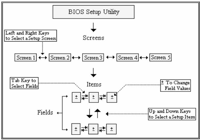
The BIOS setup/utility uses a key-based navigation system called hot keys. Most BIOS setup utility hot keys can be used at any time during setup navigation, as follows.

<table><tr><td>Key(s)</td><td>Function</td></tr><tr><td>Right Arrow, Left Arrow</td><td>Moves between different setup menus</td></tr><tr><td>Up Arrow, Down Arrow</td><td>Moves between options within a setup menu</td></tr><tr><td></td><td>Opens a submenu or displays all available settings for a highlighted configuration option</td></tr><tr><td></td><td>Returns to the previous menu and shortcuts to the Exit menu from top-level menus</td></tr><tr><td>&lt;+&gt; and &lt;--&gt;</td><td>Cycles between all available settings</td></tr><tr><td></td><td>Selects time and date fields</td></tr><tr><td></td><td>Opens the general help window for the BIOS</td></tr><tr><td></td><td>Loads previous values into the BIOS</td></tr><tr><td></td><td>Restores optimal default values into the BIOS</td></tr><tr><td></td><td>Saves the current configuration and exits BIOS setup</td></tr></table>

Table B-1: BIOS Hot Key Functions

![The flowchart describes the navigation of a BIOS Setup Utility.\n\n**Blocks:**\n*   BIOS Setup Utility\n*   Screens\n*   Left and Right Keys to Select a Setup Screen\n*   Screen 1\n*   Screen 2\n*   Screen 3\n*   Screen 4\n*   Screen 5\n*   Items\n*   Tab Key to Select Fields\n*   Fields\n*   ± To Change Field Values\n*   Up and Down Keys to Select a Setup Item\n\n**Connections:**\n*   **BIOS Setup Utility** points downward to **Screens**.\n*   **Left and Right Keys to Select a Setup Screen** connects via a dotted arrow to **Screen 1**.\n*   **Screen 1**, **Screen 2**, **Screen 3**, **Screen 4**, and **Screen 5** are arranged horizontally and connected to each other by double-headed arrows.\n*   An arrow points downward from **Screens** to **Items**.\n*   **Tab Key to Select Fields** connects via a dotted arrow to the top row of small boxes (containing a '±' symbol).\n*   **± To Change Field Values** connects via a dotted arrow to the top row of small boxes.\n*   **Fields** is a label connected by a bracket to the first box of the top row and the first box of the bottom row.\n*   **Up and Down Keys to Select a Setup Item** connects via a dotted arrow to the vertical arrows situated between the two rows of small boxes.\n*   A downward arrow connects the top row of small boxes to the bottom row of small boxes.](.pxie-39xx-tl-50m-38008-1000-10/600b7adc05202a936bfc5fa5d1f1e38668c8d9dc4438af80f2111500cee442dc.jpg)

Figure B-1: BIOS Setup Navigation

![The image displays an icon of a white document with a folded top-right corner and faint horizontal lines. A large, bold red checkmark is superimposed on the document.](.pxie-39xx-tl-50m-38008-1000-10/32b35e01c87e3346e7240cd050aa0531ea8de0201d1dedff6d0394055f9afaab.jpg)
NOTE:

A hot key legend is located in the right frame on most setup screens.

# B.3 Main

The Main Menu provides read-only information about your system and also allows you to set the System Date and Time. Refer to the tables below for details of the submenus and settings.

# B.3.1 BIOS Information

<table><tr><td>Feature</td><td>Options</td><td>Description</td></tr><tr><td>BIOS Vendor</td><td>Info only</td><td>American Megatrends</td></tr><tr><td>BIOS Version</td><td>Info only</td><td>Displays BIOS version</td></tr><tr><td>Build Date</td><td>Info only</td><td>Date the ADLINK BIOS was built</td></tr><tr><td>MRC Version</td><td>Info only</td><td>Displays MRC version</td></tr><tr><td>GOP Version</td><td>Info only</td><td>Displays GOP version</td></tr><tr><td>ME FW Version</td><td>Info only</td><td>Displays ME FW version</td></tr><tr><td>BIOS Boot Source</td><td>Info only</td><td>Primary BIOS</td></tr></table>

# B.3.2 System Information

<table><tr><td>Feature</td><td>Options</td><td>Description</td></tr><tr><td>Project Name</td><td>Info only</td><td>Displays model name</td></tr><tr><td>CPU Board Version</td><td>Info only</td><td>Displays CPU board version</td></tr><tr><td>CPU Brand String</td><td>Info only</td><td>Displays CPU model name</td></tr><tr><td>Stepping</td><td>Info only</td><td>Displays CPU stepping</td></tr><tr><td>CPU Frequency</td><td>Info only</td><td>Displays CPU frequency</td></tr><tr><td>Total Memory</td><td>Info only</td><td>Displays installed memory size</td></tr><tr><td>Memory Frequency</td><td>Info only</td><td>Displays memory frequency</td></tr><tr><td>PCH SKU</td><td>Info only</td><td>Displays PCH SKU</td></tr></table>

# B.3.3 System Management

Board Information

<table><tr><td>Board Information</td><td>Info only</td><td>Description</td></tr><tr><td>SEMA Firmware</td><td>Read only</td><td>Displays SEMA firmware</td></tr><tr><td>Build Date</td><td>Read only</td><td>Displays SEMA firmware build date</td></tr><tr><td>Serial Number</td><td>Read only</td><td>Displays SEMA S/N</td></tr><tr><td>Manufacturing Date</td><td>Read only</td><td>Displays SEMA manufacture date</td></tr><tr><td>Last Repair Date</td><td>Read only</td><td>Displays last SEMA repair date</td></tr><tr><td>MAC ID</td><td>Read only</td><td>Displays SMC MAC ID</td></tr></table>

Temperatures

<table><tr><td>Feature</td><td>Options</td><td>Description</td></tr><tr><td>Temperatures</td><td colspan="2">Info only</td></tr><tr><td>CPU Temperature</td><td colspan="2">Info only</td></tr><tr><td>Current</td><td>Read only</td><td>Displays current CPU temperature</td></tr><tr><td>Startup</td><td>Read only</td><td>Displays CPU startup temperature</td></tr><tr><td>Min</td><td>Read only</td><td>Displays min. CPU temperature</td></tr><tr><td>Max</td><td>Read only</td><td>Displays max. CPU temperature</td></tr><tr><td>Board Temperatures</td><td colspan="2">Info only</td></tr><tr><td>Current</td><td>Read only</td><td>Displays current board temperature</td></tr><tr><td>Startup</td><td>Read only</td><td>Displays board startup temperature</td></tr><tr><td>Min</td><td>Read only</td><td>Displays min. board temperature</td></tr><tr><td>Max</td><td>Read only</td><td>Displays max. board temperature</td></tr></table>

Power Consumption

<table><tr><td>Feature</td><td>Options</td><td>Description</td></tr><tr><td>Power Consumption</td><td colspan="2">Info only</td></tr><tr><td>Main Current</td><td>Read only</td><td>Displays input current</td></tr><tr><td>Current Input Power</td><td>Read only</td><td>Displays input power</td></tr><tr><td>RTC Options</td><td>Read only</td><td>Displays actual voltage of the RTC</td></tr><tr><td>5VSB</td><td>Read only</td><td>Displays actual voltage of the 5VSB</td></tr><tr><td>VIN</td><td>Read only</td><td>Displays actual voltage of the VIN</td></tr><tr><td>3.3V</td><td>Read only</td><td>Displays actual voltage of the 3.3V</td></tr><tr><td>VMEM</td><td>Read only</td><td>Displays actual voltage of the VMEM</td></tr><tr><td>3.3VSB</td><td>Read only</td><td>Displays actual voltage of the 3.3VSB</td></tr><tr><td>VCORE</td><td>Read only</td><td>Displays actual voltage of the VCC_CORE</td></tr></table>

Runtime Statistics

<table><tr><td>Feature</td><td>Options</td><td>Description</td></tr><tr><td>Runtime Statistics</td><td colspan="2">Info only</td></tr><tr><td>Total Runtime</td><td>Read only</td><td>The returned value specifies the total time in minutes the system is running in S0 state</td></tr><tr><td>Current Runtime</td><td>Read only</td><td>The returned value specifies the time in seconds the system is running in S0 state, where the counter is cleared when the system is removed from the external power supply</td></tr><tr><td>Power Cycles</td><td>Read only</td><td>The returned value specifies the number of times the external power supply has been shut down</td></tr><tr><td>Boot Cycles</td><td>Read only</td><td>Boot count is increased after a HW- or SW-Reset or successful power-up</td></tr><tr><td>Boot Reason</td><td>Read only</td><td>Shows the event responsible for reboot of the system</td></tr></table>

SEMA Flags

<table><tr><td>Feature</td><td>Options</td><td>Description</td></tr><tr><td>Flags</td><td colspan="2">Info only</td></tr><tr><td>SEMA Flags</td><td>Read only</td><td></td></tr><tr><td>BIOS Select</td><td>Read only</td><td>Displays the current selection of BIOS ROM</td></tr><tr><td>ATX/AT-Mode</td><td>Read only</td><td>Displays ATX/AT mode</td></tr></table>

Power Up

<table><tr><td>Feature</td><td>Options</td><td>Description</td></tr><tr><td>Power Up</td><td colspan="2">Info only</td></tr><tr><td>Power-up Mode(only in effect if the module is in ATX-Mode)</td><td>Turn onRemain offLast State</td><td>Turn On: The machine starts automatically when the power supply is turned on.Remain Off: To start the machine the power button has to be pressed.Last State: when powered on during a power failure the system will automatically power on when power is restored</td></tr></table>

System Date and Time

<table><tr><td>Feature</td><td>Options</td><td>Description</td></tr><tr><td>System Date</td><td>Weekday, MM/DD/YYYY</td><td>Requires alpha-numeric entry of the day of the week, day of the month, calendar month, and all 4 digits of the year, indicating the century and year (Fri XX/XX/20XX)</td></tr><tr><td>System Time</td><td>HH/MM/SS</td><td>Presented as a 24-hour clock in hours, minutes, and seconds</td></tr></table>

# B.4 Advanced

Provides settings for most user interfaces in the system.

B.4.1 CPU Configuration

<table><tr><td>Feature</td><td>Options</td><td>Description</td></tr><tr><td>Type</td><td>Info only</td><td>Displays CPU model name</td></tr><tr><td>Speed</td><td>Info only</td><td>Displays CPU frequency</td></tr><tr><td>ID</td><td>Info only</td><td>Displays CPU ID</td></tr><tr><td>Stepping</td><td>Info only</td><td>Displays CPU stepping level</td></tr><tr><td>Number of Processors</td><td>Info only</td><td>Displays number of CPU processors</td></tr><tr><td>Microcode Revision</td><td>Info only</td><td>Displays microcode revision</td></tr><tr><td>GT info</td><td>Info only</td><td></td></tr><tr><td>eDRAM Sizes</td><td>Info only</td><td>Displays the eDRAM sizes</td></tr><tr><td>L1 Instruction Cache</td><td>Info only</td><td>Displays the L1 cache size</td></tr><tr><td>L2 Cache</td><td>Info only</td><td>Displays the L2 cache size</td></tr><tr><td>L3 Cache</td><td>Info only</td><td>Displays the L3 cache size</td></tr><tr><td>L4 Cache</td><td>Info only</td><td>Displays the L4 cache size</td></tr><tr><td>VMX</td><td>Info only</td><td>Displays presence/absence of Intel Virtualization Technology support</td></tr><tr><td>SMX/TXT</td><td>Info only</td><td>Displays presence/absence of Intel SMX Technology support</td></tr><tr><td>VT-d</td><td>Disabled Enabled</td><td>Enables/disables VT-d function on MCH</td></tr><tr><td>Intel (VMX) Virtualization Technology</td><td>Disabled Enabled</td><td>Enables/disables support for Intel Virtualization technology</td></tr><tr><td>Active processor cores</td><td>Disabled Enabled</td><td>Enables/disables processor cores to active/inactive</td></tr><tr><td>Hyper-Threading</td><td>Disabled Enabled</td><td>Enables/disables hyper-threading</td></tr><tr><td>Intel® SpeedStep(TM)</td><td>DisabledEnabled</td><td>Allows support for more than two frequency ranges</td></tr><tr><td>Intel® Speed Shift Technology</td><td>DisabledEnabled</td><td>Enables/disables Intel®Speed Shift Technology</td></tr><tr><td>Turbo Mode</td><td>DisabledEnabled</td><td>Enables/disables Turbo mode</td></tr><tr><td>C states</td><td>DisabledEnabled</td><td>Enables/disables C state</td></tr></table>

# B.4.2 Memory Configuration

<table><tr><td>Feature</td><td>Options</td><td>Description</td></tr><tr><td>Memory RC Version</td><td>Info only</td><td>Displays Memory Reference Code version</td></tr><tr><td>Memory Speed</td><td>Info only</td><td>Displays memory frequency</td></tr><tr><td>Total Memory</td><td>Info only</td><td>Displays total memory</td></tr><tr><td>DIMM#0/1</td><td>Info only</td><td>Displays DIMM#0/1</td></tr><tr><td>Memory Timings (tCL-tRCD-tRP-tRAS)</td><td>Info only</td><td>Displays memory timings</td></tr></table>

# B.4.3 Graphics Configuration

<table><tr><td>Feature</td><td>Options</td><td>Description</td></tr><tr><td>GTT Size</td><td>2MB4MB8MB</td><td>Selects Graphics Translation Table size</td></tr><tr><td>Aperture Size</td><td>128MB256MB512M1024MB2048MB4096MB</td><td>Selects Aperture size.</td></tr><tr><td>DVMT Pre-Allocated</td><td>default:60MBoptions:4MB to 160MB</td><td>Selects DVMT Pre-Allocated (Fixed) Graphics Memory size used by the Internal Graphics Device</td></tr></table>

B.4.4 Onboard Devices Configuration

<table><tr><td>Feature</td><td>Options</td><td>Description</td></tr><tr><td>Serial Port Configuration</td><td>Info only</td><td></td></tr><tr><td>COM Device Settings</td><td>Info only</td><td>Serial port I/O address and IRQ</td></tr><tr><td>COM Control</td><td>RS232RS422RS485</td><td>Selects serial port mode, from among RS232, RS422, and RS485</td></tr><tr><td>LAN Port Configuration</td><td>Info only</td><td></td></tr><tr><td>LAN1 Controller</td><td>EnabledDisabled</td><td>Enables/disables onboard I225 LAN controller</td></tr><tr><td>LAN2 Controller</td><td>EnabledDisabled</td><td>Enables/disables onboard I210 LAN controller</td></tr><tr><td>SATA Configuration</td><td>Info only</td><td></td></tr><tr><td>SATA Controller(s)</td><td>EnabledDisabled</td><td>Enables/disables SATA device</td></tr><tr><td>Serial ATA Port X</td><td>Info only</td><td>Installed SATA device name</td></tr><tr><td>Software Preserve</td><td>Info only</td><td>Bootable OS in installed SATA device</td></tr><tr><td>Port X</td><td>DisabledEnabled</td><td>Enables/disables SATA port</td></tr></table>

B.4.5 USB Configuration

<table><tr><td>Feature</td><td>Options</td><td>Description</td></tr><tr><td>USB Configuration</td><td>Submenu</td><td></td></tr><tr><td>USB Module Version</td><td>Info only</td><td></td></tr><tr><td>USB Devices</td><td>Info only</td><td>Lists USB-connected peripheral devices</td></tr><tr><td>Legacy USB Support</td><td>EnabledDisabledAuto</td><td>Enables legacy USB support, where Auto disables legacy support if no USB devices are connected, and Disable retains USB devices only for EFI applications and setup</td></tr><tr><td>XHCI Hand-off</td><td>EnabledDisabled</td><td>A workaround for OS without XHCI hand-off support. XHCI ownership change should be claimed by the XHCI OS driver</td></tr><tr><td>USB Mass Storage Driver Support</td><td>EnabledDisabled</td><td>Enables/disables USB Mass Storage driver support</td></tr><tr><td>Device reset time-out</td><td>10 sec20 sec30 sec40 sec</td><td>USB mass storage device Start Unit command timeout</td></tr><tr><td>Device power-up delay</td><td>AutoManual</td><td>Maximum time before the device properly reports itself to the Host Controller. &#x27;Auto&#x27; uses default value: for a Root port, 100 ms, for a Hub port the delay is taken from the Hub descriptor</td></tr></table>

B.4.6 Network Stack Configuration

<table><tr><td>Feature</td><td>Options</td><td>Description</td></tr><tr><td>Network Stack</td><td>Enabled Disabled</td><td>Enables/disables UEFI network stack.</td></tr><tr><td>IPv4 PXE Support</td><td>Enabled Disabled</td><td>Enables/disables IPv4 PXE boot support.</td></tr><tr><td>IPv6 PXE Support</td><td>Enabled Disabled</td><td>Enables/disables IPv6 PXE boot support.</td></tr><tr><td>PXE boot wait time</td><td>0 sec</td><td>Wait time for ESC key to abort PXE boot</td></tr></table>

# B.4.7 Advanced Power Management

<table><tr><td>Feature</td><td>Options</td><td>Description</td></tr><tr><td>Advanced Power Management</td><td colspan="2">Info only</td></tr><tr><td>RTC Wake system from S5</td><td>Disabled Fixed Time Dynamic Time</td><td>Enables/disables system wake on alarm event, from among Fixed Time, where system wakes at the setting time, and Dynamic Time, in which system wakes at setting time later</td></tr></table>

# B.4.8 Hardware Health Configuration

<table><tr><td>Feature</td><td>Options</td><td>Description</td></tr><tr><td>System Health Status</td><td colspan="2">Info only</td></tr><tr><td>Ambient temp of PCIe switch</td><td>Info only</td><td>Ambient temperature near PCIe switch</td></tr><tr><td>Core temp of PCIe switch</td><td>Info only</td><td>Core temperature of PCIe switch</td></tr><tr><td>+3.3V(System)</td><td>Info only</td><td>System +3.3V voltage</td></tr><tr><td>+5V(System)</td><td>Info only</td><td>System +5V voltage</td></tr><tr><td>+12V(System)</td><td>Info only</td><td>System +12V voltage</td></tr><tr><td>VBAT</td><td>Info only</td><td>Battery voltage</td></tr></table>

# B.4.9 PXIe Links Control Configuration

<table><tr><td>Feature</td><td>Options</td><td>Description</td></tr><tr><td>Link Configuration</td><td>Info only</td><td>PCI Express link configuration to PXIe chassis</td></tr><tr><td>Link 1 Width, Speed</td><td>Info only</td><td>Link lanes and mode</td></tr><tr><td>Max Link Speed</td><td>AutoGen1Gen2Gen3</td><td>Maximum PCI Express link mode for Link 1</td></tr><tr><td>Link 2 Width, Speed</td><td>Info only</td><td>Link lanes and mode</td></tr><tr><td>Max Link Speed</td><td>AutoGen1Gen2Gen3</td><td>Maximum PCI Express link mode</td></tr></table>

# B.5 Boot

B.5.1 Boot Configuration

<table><tr><td>Feature</td><td>Options</td><td>Description</td></tr><tr><td>Boot Configuration</td><td colspan="2">Info only</td></tr><tr><td>Setup Prompt Timeout</td><td>1</td><td>Enables/disables onboard SATA controllers</td></tr><tr><td>Bootup NumLock State</td><td>Off</td><td>Selects keyboard NumLock state at boot</td></tr><tr><td>Quiet Boot</td><td>Disabled Enabled</td><td>Enables/disables PATA port, enabling/disabling the SATA channel to which the onboard SATA to PATA converter is attached. When Enabled, system boot is delayed for the time specified in PATA Port Detection Timeout if no PATA device is connected, and Auto scans for PATA device and enables by default.</td></tr><tr><td>CSM Configuration</td><td>Submenu</td><td></td></tr><tr><td>Fast Boot</td><td>Disabled Enabled</td><td>Defines the maximum time to wait for drive detection on PATA port</td></tr><tr><td>Boot Mode Select</td><td>UEFI Legacy</td><td></td></tr><tr><td>Boot Option</td><td></td><td></td></tr></table>

B.5.2 CSM Configuration

<table><tr><td>Feature</td><td>Options</td><td>Description</td></tr><tr><td>CSM Support</td><td>EnabledDisable</td><td>Determines whether CSM will launch</td></tr><tr><td>CSM16 Module Version</td><td colspan="2">Info only</td></tr><tr><td>GateA20 Active</td><td>Upon RequestAlways</td><td>Selected from among UPON REQUEST, in which GA20 can be disabled using BIOS services, and ALWAYS, in which GA20 cannot be disabled, useful when any RT code is executed above 1MB</td></tr><tr><td>INT19 Trap Response</td><td>ImmediatePostponed</td><td>BIOS reaction on INT19 trapping by Option ROM, where IMMEDIATE executes trap immediately and POSTPONED executes trap during legacy boot</td></tr><tr><td>Boot Option filter</td><td>UEFI andLegacyLegacy onlyUEFI only</td><td>Controls to which devices the system can boot</td></tr><tr><td>Option ROM execution</td><td colspan="2">Info only</td></tr><tr><td>Network</td><td>Do not launchLegacy onlyUEFI only</td><td>Controls execution of UEFI and Legacy PXE OpROM.</td></tr><tr><td>Storage</td><td>Do not launchUEFILegacy only</td><td>Controls execution of UEFI and Legacy Storage OpROM.</td></tr><tr><td>Video</td><td>Do not launchUEFILegacy only</td><td>Controls execution of UEFI and Legacy Video OpROM</td></tr><tr><td>Other PCI devices</td><td>UEFILegacy OpROM</td><td>For PCI devices other than Network, Mass storage or Video, defines the OpROM to launch.</td></tr></table>

# B.6 Security

B.6.1 Password Description

<table><tr><td>Feature</td><td>Options</td><td>Description</td></tr><tr><td>Administrator Password</td><td>Enter password</td><td></td></tr><tr><td>User Password</td><td>Enter password</td><td></td></tr><tr><td>HDD Security Configuration</td><td></td><td></td></tr><tr><td>Secure Boot</td><td>Disable Enable</td><td>Enables/disables</td></tr><tr><td colspan="3">Password DescriptionIf ONLY the Administrator&#x27;s password is set, then this only limits access to BIOS setup menu and is only asked for when entering BIOS setup menu. If ONLY the User&#x27;s password is set, then this is a power on password and must be entered to boot or enter BIOS setup menu. In BIOS setup menu the User will have Administrator rights.</td></tr></table>

# B.7 Save & Exit

<table><tr><td>Feature</td><td>Options</td><td>Description</td></tr><tr><td>Save Options</td><td colspan="2">Info only</td></tr><tr><td>Save Changes and Exit</td><td></td><td>Saves changes and exits system setup</td></tr><tr><td>Discard Changes and Exit</td><td></td><td>Discards changes and exits system setup</td></tr><tr><td>Save Changes and Reset</td><td></td><td>Saves changes and resets system</td></tr><tr><td>Discard Changes and Reset</td><td></td><td>Discards changes and resets system</td></tr><tr><td>Save Changes</td><td></td><td>Save changes made so far to Setup options</td></tr><tr><td>Discard Changes</td><td></td><td>Discards Changes made so far to Setup options</td></tr><tr><td>Default Options</td><td colspan="2">Info Only</td></tr><tr><td>Restore Defaults</td><td></td><td>Restores/loads Default values for all Setup options</td></tr><tr><td>Save as User Defaults</td><td></td><td>Saves changes made so far as User Defaults</td></tr><tr><td>Restore User Defaults</td><td></td><td>Restores User Defaults to all Setup options</td></tr><tr><td>Boot Override</td><td colspan="2">Info Only</td></tr><tr><td>Launch EFI Shell from filesystem device</td><td></td><td>Attempts to launch EFI shell application (shell.efi) from an available filesystem device</td></tr></table>

# Appendix C Dual BIOS

Dual BIOS is a backup function that maintains normal operation of the PXIe system module when unexpected boot failure occurs under the default BIOS. Dual BIOS consists of a main BIOS, a backup BIOS, and an independent controller. In normal boot, the main BIOS powers on and boots the system into the OS, monitored by the independent controller. If the main BIOS malfunctions, for example, as the result of corruption incurred by a failed update, boot procedure is terminated abnormally. The backup BIOS is then activated automatically to perform boot procedure. When backup BIOS is activated, during BIOS power-on, notifications are generated indicating that backup BIOS has been deployed. To restore main BIOS function, contact technical support.

This page intentionally left blank.

# Important Safety Instructions

For user safety, please read and follow all instructions, Warnings, Cautions, and Notes marked in this manual and on the associated device before handling/operating the device, to avoid injury or damage.

S'il vous plaît prêter attention stricte à tous les avertissements et mises en garde figurant sur l'appareil , pour éviter des blessures ou des dommages.

 Read these safety instructions carefully
 Keep the User’s Manual for future reference
 Read the Specifications section of this manual for detailed information on the recommended operating environment
 The device can be operated at an ambient temperature of 50ºC
When installing/mounting or uninstalling/removing device; or when removal of a chassis cover is required for user servicing (See “Getting Started” on page 17.):

 Turn off power and unplug any power cords/cables
 Reinstall all chassis covers before restoring power

 To avoid electrical shock and/or damage to device:

 Keep device away from water or liquid sources
 Keep device away from high heat or humidity
 Keep device properly ventilated (do not block or cover ventilation openings)
 Always use recommended voltage and power source settings
 Always install and operate device near an easily accessible electrical outlet
 Secure the power cord (do not place any object on/over the power cord)
 Only install/attach and operate device on stable surfaces and/or recommended mountings

 If the device will not be used for long periods of time, turn off and unplug from its power source

 Never attempt to repair the device, which should only be serviced by qualified technical personnel using suitable tools
 A Lithium-type battery may be provided for uninterrupted backup or emergency power.

![The image displays a safety warning label. It features a yellow equilateral triangle with a black border containing a large black exclamation point in the center. Directly below the triangle is the text 'CAUTION:' printed in black capital letters on a white background.](.pxie-39xx-tl-50m-38008-1000-10/83f01d2455550058946c37c736ac4be186611c8bc4dbcb70ff20949a393278f9.jpg)

Risk of explosion if battery is replaced with one of an incorrect type; please dispose of used batteries appropriately.

Risque d’explosion si la pile est remplacée par une autre de type incorrect. Veuillez jeter les piles usagées de façon appropriée.

 The device must be serviced by authorized technicians when:

 The power cord or plug is damaged
 Liquid has entered the device interior
 The device has been exposed to high humidity and/or moisture
 The device is not functioning or does not function according to the User’s Manual
 The device has been dropped and/or damaged and/or shows obvious signs of breakage

Disconnect the power supply cord before loosening the thumbscrews and always fasten the thumbscrews with a screwdriver before starting the system up
 It is recommended that the device be installed only in a server room or computer room where access is:

 Restricted to qualified service personnel or users familiar with restrictions applied to the location, reasons therefor, and any precautions required

 Only afforded by the use of a tool or lock and key, or other means of security, and controlled by the authority responsible for the location.

![Warning sign depicting steam rising from a plateau, indicating hazardous or hazardous material](.pxie-39xx-tl-50m-38008-1000-10/28416c05ecf9c6d5085b88ccbd7334e60382ce82fbcd06568b76d0c3c9610fa6.jpg)

# BURN HAZARD

Touching this surface could result in bodily injury.

To reduce risk, allow the surface to cool before touching.

# RISQUE DE BRÛLURES

Ne touchez pas cette surface, cela pourrait entraîner des blessures.

Pour éviter tout danger, laissez la surface refroidir avant de la toucher.

# Getting Service

Ask an Expert: https://www.adlinktech.com/en/Askanexpert

# ADLINK Technology, Inc.

No. 66, Huaya 1st Road, Guishan District

Taoyuan City 333, Taiwan

Tel: +886-3-216-5088

Fax: +886-3-328-5723

Email: service@adlinktech.com

# Ampro ADLINK Technology, Inc.

6450 Via Del Oro, San Jose,

CA 95119, USA

Tel: +1-408-360-0200

Toll Free: +1-800-966-5200 (USA only)

Fax: +1-408-600-1189

Email: info@adlinktech.com

# ADLINK Technology (China) Co., Ltd.

300 Fang Chun Rd., Zhangjiang Hi-Tech Park

Pudong New Area, Shanghai, 201203 China

Tel: +86-21-5132-8988

Fax: +86-21-5132-3588

Email: market@adlinktech.com

# ADLINK Technology GmbH

Hans-Thoma-Straße 8-10,

68163 Mannheim, Germany

Tel: +49-621-43214-0

Fax: +49-621 43214-30

Email: emea@adlinktech.com

Please visit the Contact page at www.adlinktech.com for information on how to contact the ADLINK regional office nearest you.
[🔗 Link to the original document](.pxie-39xx-tl-50m-38008-1000-10/pxie-39xx-tl-50m-38008-1000-10.pdf)