# PXIe-9852

2-CH 14-Bit 200 MS/s Digitizer

User's Manual

![Exterior view of a ADLINK Technology Inc. device with visible ports, connectors, and a black clip (no readable text or symbols beyond branding)](.pxie-9852-50-17047-1000-200-en/3b0120c9f3b2ac1ba466b1e2d7f3b7331eb261e41b2d2957b3b5b29a27d08b44.jpg)

Manual Rev.: 2.00

Revision Date: Dec. 29, 2013

Part No: 50-17047-1000

![Circular black-and-white recycling symbol with three white arrows forming a cycle (no text or symbols)](.pxie-9852-50-17047-1000-200-en/6eab416dcbc5f81f4423d3f94e08416ef0c2febe84c3509300f3dab3b0ffd34b.jpg)

Recycled Paper

# Revision History

<table><tr><td>Revision</td><td>Release Date</td><td>Description of Change(s)</td></tr><tr><td>2.00</td><td>12/29/2013</td><td>Initial Release</td></tr></table>

# Preface

# Copyright 2014 ADLINK Technology, Inc.

This document contains proprietary information protected by copyright. All rights are reserved. No part of this manual may be reproduced by any mechanical, electronic, or other means in any form without prior written permission of the manufacturer.

# Disclaimer

The information in this document is subject to change without prior notice in order to improve reliability, design, and function and does not represent a commitment on the part of the manufacturer.

In no event will the manufacturer be liable for direct, indirect, special, incidental, or consequential damages arising out of the use or inability to use the product or documentation, even if advised of the possibility of such damages.

# Environmental Responsibility

ADLINK is committed to fulfill its social responsibility to global environmental preservation through compliance with the European Union's Restriction of Hazardous Substances (RoHS) directive and Waste Electrical and Electronic Equipment (WEEE) directive. Environmental protection is a top priority for ADLINK. We have enforced measures to ensure that our products, manufacturing processes, components, and raw materials have as little impact on the environment as possible. When products are at their end of life, our customers are encouraged to dispose of them in accordance with the product disposal and/or recovery programs prescribed by their nation or company.

# Conventions

Take note of the following conventions used throughout this manual to make sure that users perform certain tasks and instructions properly.

![This image shows a white document icon with its top-right corner folded over. The document has faint horizontal gray lines and features a large, bold red checkmark in the center.](.pxie-9852-50-17047-1000-200-en/8fe56cc7ddfe99d30a5338a9c5c7c12d3d286adb4327a9a5a439663f6db25646.jpg)
NOTE:

Additional information, aids, and tips that help users perform tasks.

![The image shows a yellow triangular warning sign with a black border and a central black exclamation point. Below the sign, the word 'CAUTION:' appears in black capital letters.](.pxie-9852-50-17047-1000-200-en/b6c0fa28ff84d04f7fe4daf9d04c362743d33531576332a05af8ba6b57da0957.jpg)

Information to prevent minor physical injury, component damage, data loss, and/or program corruption when trying to complete a task.

![The image features a triangular warning sign. It has a red border and a dark red interior containing a white exclamation point. Below the triangle, the word 'WARNING' is displayed in white, uppercase letters on a black background.](.pxie-9852-50-17047-1000-200-en/10d37ff056f6640429c859ff74877cda19ea069a094f8315506034ea0c90d61d.jpg)

Information to prevent serious physical injury, component damage, data loss, and/or program corruption when trying to complete a specific task.

# Table of Contents

# Preface .... iii

# List of Figures ...... vii

# List of Tables ix

# 1 Introduction ...... 1

1.1 Features.... 1
1.2 Applications 2
1.3 Specifications.... 2

1.3.1 Analog Input 2
1.3.2 Timebase 4
1.3.3 Triggers 5
1.3.4 General Specifications....6

1.4 Software Support 7

1.4.1 SDK 7
1.4.2 WD-DASK....7

1.5 Device Layout and I/O Array 8

# 2 Getting Started 11

2.1 Installation Environment 11
2.2 Installing the Module.... 12

# 3 Operations 15

3.1 Functional Block Diagram.... 15
3.2 Analog Input Channel 15

3.2.1 Analog Input Front-End Configuration 15
3.2.2 Input Range and Data Format 16
3.2.3 DMA Data Transfer....16

3.3 Trigger Source and Trigger Modes.... 18

3.3.1 Software Trigger 19

3.3.2 External Digital Trigger 19
3.3.3 PXI STAR Trigger 19
3.3.4 PXle\_DSTARB Trigger 20
3.3.5 PXI Trigger Bus 20
3.3.6 Analog Trigger 20
3.3.7 Trigger Export 21

# 3.4 Trigger Modes 21

3.4.1 Post Trigger Mode 21
3.4.2 Delayed Trigger Mode 21
3.4.3 Pre-Trigger Mode....22
3.4.4 Middle Trigger Mode....23
3.4.5 Acquisition with Re-Triggering 23
3.4.6 Data Average Mode (Post-Trigger and Delayed-Trigger only) 24

# 3.5 Timebase 25

3.5.1 Internal Reference Clock 25
3.5.2 External Reference Clock 25
3.5.3 External Sampling Clock....25
3.5.4 PXI\_CLK10 Clock 26
3.5.5 PXI\_CLK100 Clock 26

# 3.6 ADC Timing Control 26

3.6.1 Timebase Architecture....26
3.6.2 Basic Acquisition Timing....26

# 3.7 Synchronizing Multiple Modules 29

# A Appendix: Calibration.... 31

A.1 Calibration Constant 31
A.2 Auto-Calibration 31

# Important Safety Instructions.... 33

# Getting Service 35

# List of Figures

Figure 1-1: Analog Input Channel Bandwidth, ±0.2 Vpp....3

Figure 1-2: Analog Input Channel Bandwidth, ±2 Vpp......4

Figure 1-3: PXIe-9852 Schematic....8

Figure 1-4: PXIe-9852 I/O Array 9

Figure 3-1: Analog Input Architecture of the PXIe-9852 ...... 15

Figure 3-2: Linked List of PCI Address DMA Descriptors ..... 18

Figure 3-3: Trigger Architecture of the PXIe-9852....18

Figure 3-4: External Digital Trigger 19

Figure 3-5: Post-Trigger Acquisition 21

Figure 3-6: Delayed Trigger Mode Acquisition....22

Figure 3-7: Pre-Trigger Mode Acquisition 22

Figure 3-8: Middle Trigger Mode Acquisition ....23

Figure 3-9: Re-Trigger Mode Acquisition 24

Figure 3-10: PXIe-9852 Clock Architecture 25

Figure 3-11: PXIe-9852 Timebase Architecture....26

Figure 3-12: Basic Digitizer Acquisition Timing....27

Figure 3-13: Varying Sampling Rates by Adjusting Scan Interval Counter28

This page intentionally left blank.

# List of Tables

Table 1-1: Timebase....5
Table 1-2: Trigger Source & Mode......5
Table 1-3: Digital Trigger Input 5
Table 1-4: Digital Trigger Output....6
Table 1-5: PXIe-9852 I/O Array Legend 10
Table 3-1: Input Range and Data Format....16
Table 3-2: Input Range FSR and -FSR Values....16
Table 3-3: Input Range Midscale Values....16
Table 3-4: Counter Parameters and Description ...... 29

This page intentionally left blank.

# 1 Introduction

The PXIe-9852 is a high-speed 2-CH 14-Bit 200 MS/s digitizer, specifically designed for applications such as LIDAR testing, optical fiber testing and radar signal acquisition. Analog input with 90 MHz bandwidth receives $\pm10V$ high speed signals with 50 $\Omega$ impedance, and a simplified front-end design and highly stable onboard reference provide both highly accurate measurement results and high dynamic performance.

Ideal for environments requiring real-time acquisition and transfer of data, the PXIe-9852 is based on the PCI Express Gen 2 x4 bus as interface. When signals are converted from analog to digital, continual data transfer to host system memory is enabled by PCI Express high bandwidth capability.

The PXIe-9852 is auto-calibrated with an onboard reference circuit calibrating offset and acquiring analog input errors. Following auto-calibration, the calibration constant is stored in EEPROM, such that these values can be loaded and used as needed by the board. There is no requirement to calibrate the module manually.

# 1.1 Features

▶ PXI Express specification Rev. 1.0 compliant
▶ Up to 200 MS/s sampling rate
▶ 2 simultaneous analog inputs
▶ High resolution 14-Bit ADC
▶ Up to 90 MHz bandwidth for analog input
▶ One GB onboard storage memory
▶ Scatter-Gather DMA data transfer for high-speed data streaming
▶ Supports signal averaging
▶ Support for:

▶ one external digital trigger input
▶ one digital trigger output to external instrument
▷ one external clock input
▷ auto-calibration

# 1.2 Applications

▶ Distributed Temperature Sensing (DTS)
▶ Video IC testing
▶ Physics laboratory and research environments
▶ Cable fault location and partial discharge monitoring for power applications

# 1.3 Specifications

# 1.3.1 Analog Input

<table><tr><td colspan="2">Channel Characteristics</td><td>Comment</td></tr><tr><td>Channels</td><td>2 single-ended</td><td></td></tr><tr><td>Connector type</td><td>SMA</td><td></td></tr><tr><td>Input coupling</td><td>AC or DC, software selectable</td><td></td></tr><tr><td>AC coupling cutoff frequency</td><td>11 Hz</td><td></td></tr><tr><td>ADC resolution</td><td>14-Bit</td><td></td></tr><tr><td>Input signal range</td><td>±0.2V, ±2V or ±10V</td><td></td></tr><tr><td>Bandwidth (-3dB)</td><td>90 MHz</td><td></td></tr><tr><td rowspan="2">Overvoltage</td><td>±10V</td><td>1MΩ</td></tr><tr><td>±10V sinewave / 7Vrms with |Peaks| &lt; 10V</td><td>50Ω</td></tr><tr><td>Input impedance</td><td>50Ω or 1MΩ, software selectable</td><td></td></tr><tr><td>Offset error</td><td>±1 mV</td><td></td></tr><tr><td>Gain error</td><td>±0.65%</td><td></td></tr><tr><td rowspan="5">SNR</td><td>56dB</td><td>1MΩ, ±0.2V</td></tr><tr><td>62dB</td><td>1MΩ, ±2V</td></tr><tr><td>62dB</td><td>1MΩ, ±10V</td></tr><tr><td>60dB</td><td>50Ω, ±0.2V</td></tr><tr><td>62dB</td><td>50Ω, ±2V</td></tr><tr><td rowspan="5">THD</td><td>-73dB</td><td>1MΩ, ±0.2V</td></tr><tr><td>-69dB</td><td>1MΩ, ±2V</td></tr><tr><td>-65dB</td><td>1MΩ, ±10V</td></tr><tr><td>-73dB</td><td>50Ω, ±0.2V</td></tr><tr><td>-69dB</td><td>50Ω, ±2V</td></tr><tr><td rowspan="5">SFDR</td><td>72dB</td><td>1MΩ, ±0.2V</td></tr><tr><td>72dB</td><td>1MΩ, ±2V</td></tr><tr><td>72dB</td><td>1MΩ, ±10V</td></tr><tr><td>68dB</td><td>50Ω, ±0.2V</td></tr><tr><td>68dB</td><td>50Ω, ±2V</td></tr><tr><td>CrossTalk</td><td>-80dB</td><td>±0.2V, ±2V</td></tr></table>

![The image displays a yellow triangular warning sign with a black border. Inside the triangle is a black exclamation point. Below the triangle, the text 'CAUTION:' is written in black capital letters.](.pxie-9852-50-17047-1000-200-en/c982fc0825cf3200b8a5dd10f34849f1dcaa14a7d1ab83682f308d84cc394c5c.jpg)

While $\pm10V$ , 50 $\Omega$ acquisition is available, overvoltage protection only applies to 7Vrms. Any $\pm10V$ sine wave with an offset or DC voltage over $\pm7V$ input can cause damage.

![| Frequency (Hz) | Magnitude (dB) |\n| -------------- | -------------- |\n| 0.1M           | 0              |\n| 0.3M           | 0              |\n| 1M             | 0              |\n| 3M             | 0              |\n| 10M            | 0              |\n| 30M            | -1             |\n| 100M           | -5             |\n| 300M           | -9             |](.pxie-9852-50-17047-1000-200-en/a510d06efb88c3e179ff41b1f398e38ebbb8a3e56347208a6ce1ccc0accbaea4.jpg)

Figure 1-1: Analog Input Channel Bandwidth, ±0.2 Vpp

![| Frequency (Hz) | Magnitude (dB) |\n| -------------- | -------------- |\n| 0.1M           | 0              |\n| 0.3M           | 0              |\n| 1M             | 0              |\n| 3M             | 0              |\n| 10M            | 0              |\n| 30M            | -1             |\n| 100M           | -4             |\n| 300M           | -9             |](.pxie-9852-50-17047-1000-200-en/59526ab9e0bb43800403225aabda40bb79d48b3d0989a4999a476b68eab23563.jpg)

Figure 1-2: Analog Input Channel Bandwidth, ±2 Vpp

# 1.3.2 Timebase

<table><tr><td colspan="2">Sample Clock</td><td>Comment</td></tr><tr><td rowspan="2">Timebase options</td><td>Internal : on board synthesizer</td><td></td></tr><tr><td>External : CLK IN (front panel), PXI_CLK10, and PXIe_CLK100</td><td></td></tr><tr><td rowspan="2">Sampling clock frequency</td><td>Internal : 200MHz</td><td>3.052kS/s to 200MS/s</td></tr><tr><td>External : 40MHz ~ 200MHz (CLK IN)</td><td></td></tr><tr><td>Timebase accuracy</td><td>&lt; ± 25ppm</td><td></td></tr><tr><td>External reference clock source</td><td>Front panel, PXI_CLK10, and PXIe_CLK100</td><td></td></tr></table>

<table><tr><td colspan="2">Sample Clock</td><td>Comment</td></tr><tr><td>External reference clock</td><td>10MHz</td><td></td></tr><tr><td>External reference clock input range</td><td>500mVpp ~ 5Vpp</td><td>AC / DC compliant, 50Ω load impedance</td></tr><tr><td>External sampling clock input range</td><td>1Vpp ~ 5Vpp</td><td>AC / DC compliant, 50Ω load impedance</td></tr></table>

Table 1-1: Timebase

# 1.3.3 Triggers

<table><tr><td colspan="2">Trigger Source &amp; Mode</td></tr><tr><td>Trigger source</td><td>Software, external digital trigger, analog trigger, PXI_STAR, PXI_trigger bus [0..7], and PXIe_DSTARB</td></tr><tr><td>Trigger mode</td><td>Post trigger, delay trigger, pre-trigger, or middle trigger, re-trigger for post trigger and delay trigger modes</td></tr></table>

Table 1-2: Trigger Source & Mode

<table><tr><td colspan="2">Digital Trigger Input</td></tr><tr><td>Sources</td><td>Front panel SMA connector</td></tr><tr><td>Compatibility</td><td>3.3 V TTL, 5 V tolerant</td></tr><tr><td>Input high threshold</td><td>2.0 V</td></tr><tr><td>Input low threshold (VIL)</td><td>0.8 V</td></tr><tr><td>Maximum input overload</td><td>-0.5 V ~ +5.5 V</td></tr><tr><td>Trigger polarity</td><td>Rising or falling edge</td></tr><tr><td>Pulse width</td><td>20 ns minimum</td></tr></table>

Table 1-3: Digital Trigger Input

<table><tr><td colspan="2">Digital Trigger Output</td></tr><tr><td>Compatibility</td><td>5 V TTL</td></tr><tr><td>Output high threshold (VOH)</td><td>2.4 V</td></tr><tr><td>Output low threshold (VOL)</td><td>0.2 V</td></tr><tr><td>Trigger polarity</td><td>Positive or negative</td></tr><tr><td>Pulse width</td><td>50 ns, 100 ns, 150 ns, 200 ns, 500 ns, 1 μs, 2 μs, 7.5 μs, and 10 μs</td></tr><tr><td>Trigger output driving capacity</td><td>Capable of driving 50Ω load</td></tr></table>

Table 1-4: Digital Trigger Output

# 1.3.4 General Specifications

<table><tr><td colspan="2">Specifications</td></tr><tr><td>Physical dimensions</td><td>160 (W) x 100 (H) mm (6.24 x 3.9 in.)</td></tr><tr><td>Bus</td><td></td></tr><tr><td>Bus interface</td><td>PCI Express Gen 2 x 4</td></tr><tr><td colspan="2">Environmental Tolerance</td></tr><tr><td>Operating</td><td>Temperature: 0°C - 55°CRelative humidity: 5% - 95%, non-condensing</td></tr><tr><td>Storage</td><td>Temperature: -20°C - +80°CRelative humidity: 5% - 95%, non-condensing</td></tr></table>

<table><tr><td colspan="2">Calibration</td></tr><tr><td>Onboard reference</td><td>+5 V and +2.5 V</td></tr><tr><td>Temperature coefficient</td><td>3.0 ppm/°C</td></tr><tr><td>Warm-up time</td><td>15 minutes</td></tr></table>

<table><tr><td colspan="3">Power Consumption</td></tr><tr><td>Power Rail</td><td>Standby Current (mA)</td><td>Full Load (mA)</td></tr><tr><td>+3.3 V</td><td>766</td><td>782</td></tr><tr><td>12 V</td><td>882</td><td>970</td></tr></table>

# 1.4 Software Support

ADLINK provides versatile software drivers and packages to suit various user approaches to building a system. Aside from programming libraries, such as DLLs, for most Windows-based systems, ADLINK also provides drivers for other application environments such as LabVIEW $^{®}$ .

All software options are included in the ADLINK All-in-One CD. Commercial software drivers are protected with licensing codes. Without the code, you may install and run the demo version for trial/demonstration purposes for only up to two hours. Contact your ADLINK dealer to purchase the software license.

# 1.4.1 SDK

For customers who want to write their own programs, ADLINK provides the following software development kits.

> DAQPilot for Windows, compatible with various application environments, such as VB.NET, VC.NET, VB/VC++, BCB, and Delphi
▶ DAQPilot for LabVIEW
▶ Toolbox adapter for MATLAB

# 1.4.2 WD-DASK

WD-DASK includes device drivers and DLL for Windows XP/7/8. DLL is binary compatible across Windows XP/7/8. This means all applications developed with WD-DASK are compatible with these Windows operating systems. The development environment may be VB, VB.NET, VC++, BCB, and Delphi, or any Windows programming language that allows calls to a DLL. The WD-DASK user and function reference manuals are on the ADLINK All-in-One CD.

# 1.5 Device Layout and I/O Array

![The image displays an icon of a white document with a folded top-right corner. Faint horizontal lines are visible on the page, resembling text or a list. A large, bold red checkmark is superimposed over the center of the document.](.pxie-9852-50-17047-1000-200-en/7fbfb7db652dd49c0f54dc5a0797eee6db532484a48f656dae70b03eed7e2fb1.jpg)
NOTE:

All dimensions are in mm

![165.04\n162.54\nADLINK\nTECHNOLOGY INC.\n100\n209.98](.pxie-9852-50-17047-1000-200-en/5afd1fd153590b80476187aff0332300e724a2e98d554577be6eaa90e8827cf0.jpg)

Figure 1-3: PXle-9852 Schematic

The PXIe-9852 I/O array is labeled to indicate connectivity, as shown.

![AADLINK\nPXIe-9852\nCH0 ○\nCH1 ○\nCLK IN\nTRG IN\nTRG OUT\nCH0\nCH1](.pxie-9852-50-17047-1000-200-en/c5e5d16171c114d7a5db634b734e4f3740cb7c2525673c1a8ce8bfa2153104bd.jpg)

Figure 1-4: PXIe-9852 I/O Array

<table><tr><td>Name</td><td>Faceplate Legend</td><td>Type</td><td>Remark</td></tr><tr><td>CH0</td><td>N/A</td><td>Blue</td><td>On indicates CH0 acquisition ongoing Off indicates CH0 acquisition stopped</td></tr><tr><td>CH1</td><td>N/A</td><td>Blue</td><td>On indicates CH1 acquisition ongoing Off indicates CH1 acquisition stopped</td></tr><tr><td>Ext. Clock Input</td><td>CLK IN</td><td rowspan="5">SMA Screw</td><td>Input for external reference clock or sample clock to digitizer</td></tr><tr><td>Ext. Digital Trigger Input</td><td>TRG IN</td><td>External digital trigger input, receiving trigger signal from external instrument and initiating acquisition</td></tr><tr><td>Trigger Output</td><td>TRG OUT</td><td>Trigger output, in which every time acquisition begins, a pulse synchronized with Timebase clock asserts and is output through this connector, at pulse width programmable from 50ns to 10μs via software</td></tr><tr><td>Analog Input</td><td>CH0</td><td>Analog input channel</td></tr><tr><td>Analog Input</td><td>CH1</td><td>Analog input channel</td></tr></table>

Table 1-5: PXIe-9852 I/O Array Legend

# 2 Getting Started

This chapter describes proper installation environment, installation procedures, package contents and basic information users should be aware of regarding the PXIe-9852.

![A graphic icon showing a piece of lined paper with a large red checkmark superimposed over the left side.](.pxie-9852-50-17047-1000-200-en/20fedb2607063cfc3b862cd267b2af1b30cb70d2c94cb541d0d87dcdc7802e65.jpg)
NOTE:

Diagrams and illustrated equipment are for reference only. Actual system configuration and specifications may vary.

# 2.1 Installation Environment

When unpacking and preparing to install, please refer to Important Safety Instructions.

Only install equipment in well-lit areas on flat, sturdy surfaces with access to basic tools such as flat- and cross-head screwdrivers, preferably with magnetic heads as screws and standoffs are small and easily misplaced.

Recommended Installation Tools

▶ Phillips (cross-head) screwdriver
▶ Flat-head screwdriver
Anti-static wrist strap
▶ Antistatic mat

ADLINK PXIe-9852 DAQ modules are electrostatically sensitive and can be easily damaged by static electricity. The module must be handled on a grounded anti-static mat. The operator must wear an anti-static wristband, grounded at the same point as the anti-static mat.

Inspect the carton and packaging for damage. Shipping and handling could cause damage to the equipment inside. Make sure that the equipment and its associated components have no damage before installation.

![A yellow triangular warning sign featuring a black exclamation mark in the center. Below the triangle, the text 'CAUTION:' is printed in black, uppercase letters.](.pxie-9852-50-17047-1000-200-en/d6a371537475a17b3e2a27e9ace49b9c9bf5d4707ca6c598d607f67f5da7bfe3.jpg)

The equipment must be protected from static discharge and physical shock. Never remove any of the socketed parts except at a static-free workstation. Use the anti-static bag shipped with the product to handle the equipment and wear a grounded wrist strap when servicing.

▶ Package Contents
▶ PXIe-9852 high-speed digitizer
▶ ADLINK All-in-one compact disc
▶ PXIe-9852 Quick Start Guide

If any of these items are missing or damaged, contact the dealer

![This image displays a safety warning sign. It features a red triangle pointing upwards containing a large white exclamation point in the center. Below the triangle is a black rectangular banner with the word 'WARNING' printed in white capital letters.](.pxie-9852-50-17047-1000-200-en/a265fdcbeaad1ae35e82ec5a2ede99716971a7438decdff9fc08720627d9419b.jpg)

Do not install or apply power to equipment that is damaged or missing components. Retain the shipping carton and packing materials for inspection. Please contact your ADLINK dealer/vendor immediately for assistance and obtain authorization before returning any product.

# 2.2 Installing the Module

1. Turn off the PXle system/chassis and connect the power cable from the power source.

![The image features a document icon with a folded upper right corner and a large red checkmark superimposed over it. The document contains ten lines of text, which read:\n\nThis is line 1\nThis is line 2\nThis is line 3\nThis is line 4\nThis is line 5\nThis is line 6\nThis is line 7\nThis is line 8\nThis is line 9\nThis is line 10](.pxie-9852-50-17047-1000-200-en/ee9804b84f6e7cc8d508c1a9e2e0a516a2b0388642bd577427d514f728424797.jpg)

Connection of the power cable provides grounding to prevent hazardous ESD (electrostatic discharge).

NOTE:

2. Align the module's edge with the module guide in the PXIe chassis.
3. Slide the module into the chassis until resistance is felt from the PXIe connector.
4. Push the ejector latch upwards and fully insert the module into the chassis.

5. Once the module is fully seated, a "click" can be heard from the ejector latch.

6. Tighten the screw on the front panel.

7. Power up the PXle system/chassis.

![The image displays an icon of a white document with a folded top-right corner. Inside the document, there are faint horizontal gray lines resembling text. A large, bold red checkmark is superimposed over the left side of the document.](.pxie-9852-50-17047-1000-200-en/bcaf43a385271ace6e0a432b65f0276ccfaede4ca7692c993f2f8dbae9756748.jpg)
NOTE:

The red ejector latch lock must be depressed before the module can be uninstalled.

This page intentionally left blank.

# 3 Operations

This chapter contains information regarding analog input, triggering and timing for the PXIe-9852.

# 3.1 Functional Block Diagram
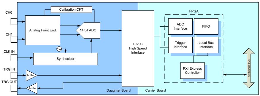
![Based on the provided block diagram, here is the accurate description of the labeled blocks and their connections:\n\n**Daughter Board Section (Blue Background)**\n*   **Inputs:** The diagram begins on the left with inputs labeled `CH0`, `CH1`, `CLK IN`, `TRG IN`, and `TRG OUT`.\n*   **Analog Processing:** `CH0` and `CH1` enter the `Analog Front End`.\n*   **Calibration:** A block labeled `Calibration CKT` connects to both the `Analog Front End` and the `14 bit ADC`.\n*   **ADC Conversion:** The `Analog Front End` outputs to the `14 bit ADC`. A `Synthesizer` (which receives `CLK IN`) provides a clock signal to the `14 bit ADC`.\n*   **Trigger Path:** `TRG IN` passes through a `buffer` and enters the `B to B High Speed Interface`.\n*   **High Speed Interface:** The `14 bit ADC` outputs to the `B to B High Speed Interface`. This interface also sends a signal through a bottom `buffer` to the `TRG OUT` port.\n\n**Carrier Board Section (Light Blue Background)**\n*   **FPGA Section:** A dashed box labeled `FPGA` contains several sub-blocks.\n*   **Connections from Interface:** The `B to B High Speed Interface` connects to the `ADC Interface` and the `Trigger Interface` inside the FPGA.\n*   **Data Path:** The `ADC Interface` connects to a `FIFO` block.\n*   **Trigger/Bus Path:** The `Trigger Interface` connects to a `Local Bus Interface`.\n*   **Controller:** A `PXI Express Controller` connects to the `Local Bus Interface`.\n*   **External Bus:** The `PXI Express Controller` connects to the `PXI Express BUS` (indicated by a vertical double-headed arrow on the far right).](.pxie-9852-50-17047-1000-200-en/dd3b0c5c4ed47638bfac6d69d3b47e890c45d7cb4bd35fa52087831f5901cecb.jpg)

# 3.2 Analog Input Channel

# 3.2.1 Analog Input Front-End Configuration

![This block diagram depicts a signal processing chain flowing from left to right. The labeled blocks and their connections are as follows:\n\n1.  **Input:** A signal enters from the left.\n2.  **Protection ckt:** The signal passes through a block labeled **'Protection ckt'**.\n3.  **Switch/Calibration:** The signal continues to an unlabeled switch block. A separate block labeled **'Calibration Source'** connects to this switch.\n4.  **AC / DC Couple:** The signal passes through a block with a capacitor symbol labeled **'AC / DC Couple'**.\n5.  **50Ω / Hi-Z:** The signal passes through a block with a resistor symbol labeled **'50Ω / Hi-Z'**.\n6.  **High Impedance Buffer:** The signal passes through a triangle block labeled **'High Impedance Buffer'**.\n7.  **1x / 10x amplifier:** The signal passes through a triangle block with a resistor symbol inside, labeled **'1x / 10x amplifier'**.\n8.  **ADC Driver:** The signal passes through a triangle block labeled **'ADC Driver'**.\n9.  **100MHz LPF:** The signal enters a rectangular block labeled **'100MHz LPF'** at pin 1. Pin 2 connects to ground. Pins 3 and 4 serve as outputs.\n10. **14-bit ADC:** The outputs from the LPF (pins 3 and 4) connect to pins 5 and 6 of a rectangular block labeled **'14-bit ADC'**.\n11. **Output:** The final signal exits from pins 7, 8, and 9 of the ADC block, represented by a line labeled **'14'** with a diagonal slash indicating a bus.](.pxie-9852-50-17047-1000-200-en/e71fad98b239ee866d53d523562871b4e33327bde932b0e9ac84604096d00f0c.jpg)

Figure 3-1: Analog Input Architecture of the PXle-9852

# Input Configuration

The input channel terminates with equivalent 50Ω or 1 MΩ input impedance (selected by software). The 14-bit ADC provides not only accurate DC performance but also high signal-to-noise ratio, and high spurious-free dynamic range in AC performance. The ADC transfers data to system memory via the high speed PCI Express Gen2 X 4 interface.

For auto-calibration, internal calibration provides stable and accurate reference voltage to the AI.

# 3.2.2 Input Range and Data Format

Data format of the PXIe-9852 is 2's complement. The ADC data of PXIe-9852 is on the 14 MSB of the 16-bit A/D data. The 2 LSB of the 16-bit A/D data should be truncated by software. A/D data structure is as follows.

<table><tr><td>D15</td><td>D14</td><td>D13</td><td>D12</td><td>....</td><td>D3</td><td>D2</td><td>D1</td><td>D0</td></tr><tr><td colspan="9">D15 ~ D2 bits represent the data from ADC (2&#x27;s complement)D1, D0 bits are always 0.</td></tr></table>

Table 3-1: Input Range and Data Format

<table><tr><td>Description</td><td>Full scale range</td><td>Least significant bit</td><td>FSR-1LSB</td><td>-FSR</td></tr><tr><td rowspan="3">Bipolar Analog Input</td><td>±10V</td><td>1.22mV</td><td>9.99878V</td><td>-10.000V</td></tr><tr><td>±2V</td><td>0.244mV</td><td>1.99976V</td><td>-2V</td></tr><tr><td>±0.2V</td><td>24.4uV</td><td>0.199976V</td><td>-0.2V</td></tr><tr><td>Digital Code</td><td>N/A</td><td>N/A</td><td>7FFC</td><td>8000</td></tr></table>

Table 3-2: Input Range FSR and -FSR Values

<table><tr><td>Description</td><td></td><td>Midscale +1LSB</td><td>Midscale</td><td>Midscale -1LSB</td></tr><tr><td rowspan="3">Bipolar Analog Input</td><td>±10V</td><td>1.22mV</td><td>0V</td><td>-1.22mV</td></tr><tr><td>±2V</td><td>0.244mV</td><td>0V</td><td>-0.244mV</td></tr><tr><td>±0.2V</td><td>24.4V</td><td>0V</td><td>-24.4μV</td></tr><tr><td>Digital Code</td><td></td><td>0004</td><td>0000</td><td>FFFC</td></tr></table>

Table 3-3: Input Range Midscale Values

# 3.2.3 DMA Data Transfer

The PXIe-9852, a PCIe Gen 2 X 4 device, is equipped with a 200MS/s high sampling rate ADC, generating a 800 MByte/second rate.

To provide efficient data transfer, a PCI bus-mastering DMA is essential for continuous data streaming, as it helps to achieve full potential PCI Express bus bandwidth. The bus-mastering controller releases the burden on the host CPU since data is directly transferred to the host memory without intervention. Once analog input operation begins, the DMA returns control of the program. During DMA transfer, the hardware temporarily stores acquired data in the onboard AD Data FIFO, and then transfers the data to a user-defined DMA buffer in the computer.

Using a high-level programming library for high speed DMA data acquisition, the sampling period and the number of conversions needs simply to be assigned into specified counters. After the AD trigger condition is met, the data will be transferred to the system memory by the bus-mastering DMA.

In a multi-user or multi-tasking OS, such as Microsoft Windows, Linux, or other, it is difficult to allocate a large continuous memory block. Therefore, the bus controller provides DMA transfer with scatter-gather function to link non-contiguous memory blocks into a linked list so users can transfer large amounts of data without being limited by memory limitations. In non-scatter-gather mode, the maximum DMA data transfer size is 2M double words (8 M bytes); in scatter-gather mode, there is no limitation on DMA data transfer size except the physical storage capacity of the system.

Users can also link descriptor nodes circularly to achieve a multi-buffered DMA. Figure 3-2 illustrates a linked list comprising three DMA descriptors. Each descriptor contains a PCI address, PCI dual address, a transfer size, and the pointer to the next descriptor. PCI address and PCI dual address support 64-bit addresses which can be mapped into more than 4 GB of address space.

![Based on the provided image, here is the accurate and concise description of the flowchart:\n\n**Labeled Blocks:**\n\n*   **Bottom Block:** 'Local Memory (FIFO)'\n*   **Middle Block (Lower):** 'PX I Express Bus'\n*   **Left Column Block:**\n    *   'First PXI Address'\n    *   'First Dual Address'\n    *   'Transfer Size'\n    *   'Next Descriptor'\n*   **Middle Column Block:**\n    *   'PX I Address'\n    *   'Dual Address'\n    *   'Transfer Size'\n    *   'Next Descriptor'\n*   **Right Column Block:**\n    *   'PX I Address'\n    *   'Dual Address'\n    *   'Transfer Size'\n    *   'Next Descriptor'\n\n**Connections:**\n\n*   An arrow points upward from 'Local Memory (FIFO)' to 'PX I Express Bus'.\n*   An arrow points upward from 'PX I Express Bus' to the bottom of the Middle Column Block.\n*   An arrow points from the Left Column Block (specifically from the 'Next Descriptor' row) to the Middle Column Block (specifically to the 'Next Descriptor' row).\n*   An arrow points from the Middle Column Block (specifically from the 'PX I Address' row) to the Right Column Block (specifically to the 'PX I Address' row).](.pxie-9852-50-17047-1000-200-en/19687e66c9699e908f1b4673ae0faf36f671516d80d65f8bc0f497fe4a93709a.jpg)

Figure 3-2: Linked List of PCI Address DMA Descriptors

# 3.3 Trigger Source and Trigger Modes

This section details PXIe-9852 triggering operations.

![The flowchart depicts a trigger routing system with the following labeled blocks and connections:\n\n**1. Trigger Source Stage**\nA trapezoidal block labeled **'Trigger source MUX'** receives the following inputs via arrows:\n*   **'Software trigger'**\n*   **'Digital Trigger In'**\n*   **'Analog trigger ch0'**\n*   **'Analog trigger ch1'**\n*   A signal from a **'TRG IN'** source symbol (circle with ground).\n*   Three signals originating from a bidirectional arrow labeled **'PXI Trigger Bus'**:\n    *   **'PXI_STAR'**\n    *   **'PXIe_DSTARB'**\n    *   **'PXI_TriggerBus(0:7)'**\n\n**2. Decision Stage**\nAn arrow connects the **'Trigger source MUX'** to a rectangular block labeled **'Trigger Decision'**.\n\n**3. Trigger Output Stage**\nAn arrow connects the **'Trigger Decision'** block to a trapezoidal block labeled **'Trigger Output MUX'**. This block has three outputs:\n*   An arrow labeled **'To Internal FPGA Circuits'** pointing upward and right.\n*   An arrow pointing to a **'TRG OUT'** source symbol (circle with ground).\n*   An arrow labeled **'SSI_TRIG1'** pointing to a bidirectional arrow labeled **'PXI Trigger Bus'**.](.pxie-9852-50-17047-1000-200-en/8919db1aedd7fa3282236fb08eb16428acf566706dc8f18bdd81dfdf951a3d24.jpg)

Figure 3-3: Trigger Architecture of the PXle-9852

The PXIe-9852 requires a trigger to implement acquisition of data. Configuration of triggers requires identification of trigger source. The PXIe-9852 supports internal software trigger, external digital trigger, and analog trigger.

# 3.3.1 Software Trigger

The software trigger, generated by software command, is asserted immediately following execution of specified function calls to begin the operation.

# 3.3.2 External Digital Trigger

An external digital trigger is generated when a TTL rising edge or falling edge is detected at the SMA connector TRG IN on the front panel. As shown, trigger polarity can be selected by software. Note that the signal level of the external digital trigger signal should be TTL compatible, and the minimum pulse width 20 ns.

![The image displays two diagrams side-by-side illustrating signal trigger events.\n\nAt the top of both diagrams is the text '**Pulse Width ) 20ns**,' situated above a horizontal double-headed arrow indicating the duration of the pulse.\n\nThe left diagram shows a square wave pulse with a vertical arrow pointing upward on the rising edge. Below the diagram is the text '**Rising Edge Trigger Event**'.\n\nThe right diagram shows a similar square wave pulse but with a vertical arrow pointing downward on the falling edge. Below the diagram is the text '**Falling Edge Trigger Event**'.](.pxie-9852-50-17047-1000-200-en/12f3f15a19ef032d3bcf3280f1f206ae4599b621feacdd47fbe502c5dca09788.jpg)
Figure 3-4: External Digital Trigger

# 3.3.3 PXI STAR Trigger

When PXI STAR is selected as the trigger source, the PXIe-9852 accepts a TTL-compatible digital signal as a trigger signal.

Triggering occurs when a rising edge or falling edge is detected at PXI STAR, with trigger polarity configurable by software. The minimum pulse width requirement of this digital trigger signal is 20 ns.

# 3.3.4 PXIe\_DSTARB Trigger

The PXIe\_DSTARB signal, a differential signal transmitted via the PXI Express Chassis backplane, distributes high-speed, high-quality trigger signals. When PXIe\_DSTARB is selected as the trigger source, the PXIe-9852 accepts a fast-switching LVDS digital signal as a trigger signal. Triggering occurs when a rising edge or falling edge is detected at PXIe\_DSTARB, with trigger polarity configurable by software, with minimum pulse width requirement of 20 ns.

# 3.3.5 PXI Trigger Bus

The PXIe-9852 utilizes PXI Trigger Bus Numbers 0 through 7 to act as a System Synchronization Interface (SSI). With the interconnected bus provided by PXI Trigger Bus, multiple modules are easily synched. When configured as input, the PXIe-9852 serves as a slave module and can accept trigger signals from one of buses 0 through 7. When configured as output, the PXIe-9852 serves as a master module and can output trigger signals to the PXI Trigger Bus Numbers 0 through 7.

# 3.3.6 Analog Trigger

An analog trigger is generated when AI input signal level is detected at the SMA connector CH0, CH1 (selected by software). The trigger level is also selected by software.

# 3.3.7 Trigger Export

When acquisition is initiated, a pulse synchronized with the Time-base clock asserts and is output through trigger output, at a pulse width programmable from 50ns to 10 $\mu$ s via software.

# 3.4 Trigger Modes

Trigger modes applied to trigger sources initiate different data acquisition timings when a trigger event occurs. The following trigger mode descriptions are applied to analog input function.

# 3.4.1 Post Trigger Mode

Post-trigger acquisition is applicable when data is to be collected after the trigger event, as shown. When the operation starts, PXIe-9852 waits for a trigger event. Once the trigger signal is received, acquisition begins. Data is generated from ADC and transferred to system memory continuously. The acquisition stops once the total data amount reaches a predefined value.

![This diagram illustrates a timing sequence with three horizontal tracks:\n\n1.  **Timeline:** A horizontal line with an arrow pointing right labeled 'Time'. Three downward arrows point to specific moments on this line, labeled 'Operation start', 'Trigger Event Occurs Acquisition start', and 'Acquisition stop'.\n2.  **Trigger:** A signal line labeled 'Trigger' displays a rectangular pulse that aligns vertically with the 'Trigger Event Occurs' point on the timeline.\n3.  **Data:** A signal line labeled 'Data' contains a rectangular block labeled 'N samples' that begins shortly after the trigger pulse and extends to the right.](.pxie-9852-50-17047-1000-200-en/fe9b73bdeef0f62e965a5dec47a8f07038631b703a651c8ebd6498032068acce.jpg)

Figure 3-5: Post-Trigger Acquisition

# 3.4.2 Delayed Trigger Mode

Delayed-trigger acquisition is utilized to postpone data collection after the trigger event, as shown. When PXIe-9852 receives a trigger event, a time delay is implemented before commencing acquisition. The delay is specified by a 16-bit counter value such that a maximum thereof is the period of TIMEBASE X ( $2^{16}$ ), and the minimum is the Timebase period.

![This image is a timing diagram illustrating a sequence of events over a horizontal 'Time' axis. It consists of three distinct rows:\n\n**1. Top Timeline:**\nA horizontal arrow labeled 'Time' points to the right. Four downward-pointing arrows mark specific moments in chronological order:\n*   'Operation start'\n*   'Trigger Event Occurs'\n*   'Acquisition start'\n*   'Acquisition stop'\n\nBetween the 'Trigger Event Occurs' marker and the 'Acquisition start' marker, there is a horizontal double-headed arrow labeled 'Delay Time'.\n\n**2. Middle Row (Trigger):**\nLabeled 'Trigger', this row shows a signal line that is flat until a single positive pulse (a rectangular wave) occurs. This pulse aligns vertically with the 'Trigger Event Occurs' marker.\n\n**3. Bottom Row (Data):**\nLabeled 'Data', this row shows a signal line that remains flat until a rectangular block appears. This block is labeled 'N samples' and spans horizontally between the vertical markers for 'Acquisition start' and 'Acquisition stop'.](.pxie-9852-50-17047-1000-200-en/093f13a47394b1c4ba42bcde51a1419c5893ce923f0fcf7f2f290992f5c03f7f.jpg)

Figure 3-6: Delayed Trigger Mode Acquisition

# 3.4.3 Pre-Trigger Mode

Collects data before the trigger event, starting once specified function calls are executed to begin the pre-trigger operation, and stopping when the trigger event occurs. If the trigger event occurs after the specified amount of data has been acquired, the system stores only data preceding the trigger event by a specified amount, as follows.

![This diagram illustrates a timing sequence for data acquisition, featuring a timeline at the top, a signal trace below it, and a data buffer at the bottom.\n\n**Timeline (Top)**\nA horizontal arrow points to the right, labeled **Time**. Three downward arrows mark specific events:\n1.  **Left Arrow:** Points to the text '**Operation start Acquisition start**'.\n2.  **Middle Arrow:** Points to the text '**Trigger signals occuring before the specified amount of data has been acquired are ignored**'. Below this text, vertical dotted lines extend down to the timeline.\n3.  **Right Arrow:** Points to the text '**Trigger Event Occurs Acquisition stop Data transfer to system begins**'.\n\n**Trigger Signal (Middle)**\nLabeled **Trigger**, this line shows a signal that is normally low. It features two positive pulses (squares):\n1.  The first pulse aligns vertically with the middle timeline event ('Trigger signals occuring...').\n2.  The second pulse aligns vertically with the right timeline event ('Trigger Event Occurs...').\n\n**Data Block (Bottom)**\nLabeled **Data**, this is a long horizontal bar divided into two sections:\n1.  **Left Section:** A hatched/shaded area. Below this section is a horizontal bracket with the text '**X samples have been acquired before trigger occurs, where X(N**'. This section aligns vertically with the start of the timeline and the first pulse on the Trigger line.\n2.  **Right Section:** A white rectangle labeled '**N samples**'. This section begins after the first pulse and ends at the vertical alignment of the second pulse (the actual trigger event).](.pxie-9852-50-17047-1000-200-en/45a2f1188958580af01fc849eaf6749b6823b66dc66726c33e262e738bb57996.jpg)

Figure 3-7: Pre-Trigger Mode Acquisition

# 3.4.4 Middle Trigger Mode

Collects data before and after the trigger event, with the amount to be collected set individually (M and N samples), as follows

![This is a timing diagram illustrating the sequence of operations for data acquisition. It consists of three rows aligned vertically:\n\n**1. Top Row (Timeline):**\n*   A horizontal arrow pointing right, labeled **'Time'**.\n*   Three downward-pointing arrows indicate specific events along the timeline:\n    *   Left: **'Operation start Acquisition start'**\n    *   Center: **'Trigger event occurs'**\n    *   Right: **'Acquisition stop Data transfer to system begins'**\n\n**2. Middle Row (Trigger Signal):**\n*   Labeled **'Trigger'** on the left.\n*   Shows a signal line that is low, then rises into a single square pulse, and returns low.\n*   The pulse aligns vertically with the **'Trigger event occurs'** arrow above it.\n\n**3. Bottom Row (Data Buffer):**\n*   Labeled **'Data'** on the left.\n*   Shows a long rectangular bar representing a data buffer, divided into three segments:\n    *   Left segment: Filled with diagonal hatching lines.\n    *   Middle segment: Labeled **'M samples'**.\n    *   Right segment: Labeled **'N samples'**.\n*   The start of the **'M samples'** segment aligns vertically with the **'Trigger event occurs'** arrow and the rising edge of the trigger pulse.\n*   The end of the **'M samples'** segment (and start of 'N samples') aligns vertically with the **'Acquisition stop Data transfer to system begins'** arrow.](.pxie-9852-50-17047-1000-200-en/76561f22480590d8156124f6621976eadcf9d62d6e2df6fe064550b2c4ca634e.jpg)

Figure 3-8: Middle Trigger Mode Acquisition

# 3.4.5 Acquisition with Re-Triggering

A digitizer acquires a trace of N samples/channel for a single acquisition. Re-Trigger mode can also be set to automatically acquire R traces, containing N\*R samples/channel of data, without additional software intervention.

The Re-Trigger setting can be used for Post-Trigger and Delayed-Trigger modes, with different limitations on the spacing between trigger events in each mode. Trigger events arriving too close to the previous instance will be ignored by the digitizer.

▶ In Post-Trigger mode, the minimum spacing between trigger events is N+8
▶ In Delayed-Trigger mode, the minimum spacing between trigger events is $(N+D)+8$ , where D is the number of the delayed setting

![This image is a timing diagram illustrating the relationship between time, trigger events, and data acquisition. It consists of three horizontal rows aligned vertically:\n\n**1. Top Row (Time Axis):**\n*   A horizontal line with an arrow pointing to the right is labeled **'Time'**.\n*   Three vertical arrows point downward onto this line, marking specific moments:\n    *   The first arrow is labeled **'Operation start'**.\n    *   The second arrow is labeled **'1st Trigger Event Occurs'**.\n    *   The third arrow is labeled **'2nd Trigger Event Occurs'**.\n\n**2. Middle Row (Trigger Signal):**\n*   Labeled **'Trigger'** on the far left.\n*   The trace shows a signal line that is normally low but features two positive rectangular pulses (high states).\n*   The first pulse aligns vertically with the **'1st Trigger Event Occurs'** label.\n*   The second pulse aligns vertically with the **'2nd Trigger Event Occurs'** label.\n\n**3. Bottom Row (Data Signal):**\n*   Labeled **'Data'** on the far left.\n*   The trace shows a signal line containing two distinct rectangular blocks.\n*   Both blocks are labeled **'N samples'**.\n*   The first block aligns with the first trigger pulse.\n*   The second block aligns with the second trigger pulse.](.pxie-9852-50-17047-1000-200-en/bba72441e0cc6804b1bff1a2da31ae094b332049300181b8296110c60c40f5fc.jpg)

Figure 3-9: Re-Trigger Mode Acquisition

# 3.4.6 Data Average Mode (Post-Trigger and Delayed-Trigger only)

In normal post-trigger mode acquisition, N samples/channel data are generated for a single trigger event. In Re-trigger mode (See "Acquisition with Re-Triggering" on page 23.), a total of N \* R samples/channel data is generated for R trigger events, that is, R traces (A trace contains N samples/channel). In Data Average Mode, only N samples/channel data are generated for R trigger events. The single trace data (N samples/channel) is the average of the R traces sample by sample.

The output data format is 16-bit or 32-bit signed integer, software selectable. When higher measurement accuracy is desired, data average mode with 32 bit data output can improve the resolution. According to oversampling practice, the retrigger times R required to get n bits of additional resolution is $R = 4^{n}$ . Please note that in order for data average mode to work properly, components of signal of interest, such as period and magnitude, should be consistent during conversion.

# 3.5 Timebase

![This block diagram illustrates a clock signal routing and conditioning system. Here are the labeled blocks and connections:\n\n**Blocks and Labels:**\n*   **CLK IN**: A clock source symbol connected to ground.\n*   **External Sampling CLK**: A signal path label.\n*   **External Reference CLK**: A signal path label.\n*   **PXIe 10MHz / Xtal 10MHz**: An input signal label.\n*   **Synthesizer**: A rectangular processing block.\n*   **PXIe 100MHz**: An input signal label.\n*   **CLK Buffer**: A triangular buffer block.\n*   **To ADC**: An output arrow label.\n\n**Connections:**\n1.  **CLK IN** connects to a switch.\n2.  This first switch has two outputs:\n    *   The top output is labeled **External Sampling CLK** and connects directly to the top input of the **CLK Buffer**.\n    *   The bottom output is labeled **External Reference CLK** and connects to the top input of a second switch.\n3.  The second switch selects between two inputs:\n    *   Top input: Connected to **External Reference CLK**.\n    *   Bottom input: Connected to **PXIe 10MHz / Xtal 10MHz**.\n    *   The output of this switch connects to the left side of the **Synthesizer**.\n4.  **PXIe 100MHz** connects to the bottom-left side of the **Synthesizer**.\n5.  The output of the **Synthesizer** connects to the bottom input of the **CLK Buffer**.\n6.  The output of the **CLK Buffer** points to the right, labeled **To ADC**.](.pxie-9852-50-17047-1000-200-en/ba8254d10d33bb712afd4bcc5c006ade306fbbb8841011d6f820d6959f443380.jpg)

Figure 3-10: PXle-9852 Clock Architecture

# 3.5.1 Internal Reference Clock

The PXIe-9852 internal 10MHz Crystal oscillator acts as reference clock, generating, after synthesis, precisely 200MHz clock for ADC.

# 3.5.2 External Reference Clock

The PXIe-9852 can choose an external clock source for use as a reference clock. When an external clock reference is selected, the synthesizer input will switch to the clock source at SMA connector CLK IN, and generate precisely 200MHz clock for ADC. The frequency of clock source is restricted to 10MHz.

# 3.5.3 External Sampling Clock

The PXIe-9852 can further choose an external clock source as ADC sampling clock. When an external sampling clock is selected, the ADC sampling frequency switches to the clock source at SMA Connector CLK IN, and clock source frequency is available from 40MHz to 200MHz.

# 3.5.4 PXI\_CLK10 Clock

The PXIe-9852 can receive the timebase from the PXI\_CLK10 Clock, the signal of which originates at the PXI Express chassis backplane, matched in propagation delay within 1 ns.

# 3.5.5 PXI\_CLK100 Clock

The PXIe-9852 can receive the timebase from the PXI\_CLK100 Clock, the signal of which originates at the PXI Express chassis backplane, matched in propagation delay within 200 ps.

# 3.6 ADC Timing Control

# 3.6.1 Timebase Architecture

![Based on the provided image, here is the accurate description of the flowchart:\n\n**Blocks and Labels:**\n*   **Onboard 200 MHz Oscillator** (Text input on the far left)\n*   **ADC** (Square block)\n*   **ADC Output 200 MHz** (Label on the connecting line)\n*   **X2 Multiplier PLL** (Square block)\n*   **400 MHz** (Label on the top output line)\n*   **For ADC Data Bus** (Text output)\n*   **200 MHz** (Label on the bottom output line)\n*   **For ADC state machine** (Text output)\n*   **FPGA** (Label below the dashed box enclosing the right side components)\n\n**Connections:**\n1.  An arrow points from **Onboard 200 MHz Oscillator** into the **ADC** block.\n2.  An arrow exits the **ADC** block labeled **ADC Output 200 MHz**.\n3.  This arrow enters a dashed box labeled **FPGA** and splits into two parallel paths.\n4.  The top path enters the **X2 Multiplier PLL** block. An arrow exits this block labeled **400 MHz**, pointing to **For ADC Data Bus**.\n5.  The bottom path bypasses the multiplier block and is labeled **200 MHz**, pointing to **For ADC state machine**.](.pxie-9852-50-17047-1000-200-en/b99aa7b7befbad66f1e6f5c831d7797f19c078403724771767e2749821fbc4ff.jpg)

Figure 3-11: PXle-9852 Timebase Architecture

# 3.6.2 Basic Acquisition Timing

The PXIe-9852 commences acquisition upon receipt of a trigger event originating with software command, external digital trigger, or the PXIe Trigger Bus. The Timebase is a clock provided to the ADC and acquisition engine for essential timing. The Timebase is from an onboard synthesizer. To achieve different sampling rates, a scan interval counter is used.

Using the post-trigger mode as an example, as shown, when a trigger is accepted by the digitizer, the acquisition engine commences acquisition of data from ADC, and stores the sampled data to the onboard FIFO. When FIFO is not empty, data will be transferred to system memory immediately through the DMA engine. The sampled data is generated continuously at the rising edge of Timebase according to the scan interval counter setting. When sampled data reaches a specified value, in this example 256, acquisition ends.

![The image is a timing diagram illustrating signal acquisition. It consists of stacked rows representing different signals and a sequence of data blocks.\n\n**Labeled Blocks and Rows:**\n*   **Analog signal**: A sine wave with black dots indicating sampling points.\n*   **TIMEBASE**: A square wave clock signal.\n*   **Trigger**: A signal line showing a pulse.\n*   **Acquisition In Progress**: A signal line that transitions from low to high.\n*   **DATA**: A horizontal sequence of hexagonal blocks labeled **D1**, **D2**, **D3**, **D4**, followed by ellipses (circles), and ending with **D253**, **D254**, **D255**, **D256**.\n\n**Text Annotations and Connections:**\n*   **Acquisition initiates following this clock edge**: An arrow points to the rising edge of the 'Acquisition In Progress' signal.\n*   **Trigger mode = post-trigger, DataCnt = 256, ScanIntrv = 1**: Text at the bottom describing the mode and parameters.\n\n**Relationships/Connections:**\n*   The black dots on the **Analog signal** are vertically aligned with the rising edges of the **TIMEBASE**, indicating that sampling occurs at these clock edges.\n*   The **DATA** sequence corresponds to the samples acquired during the 'Acquisition In Progress' phase.\n*   The **Trigger** pulse precedes the start of the 'Acquisition In Progress' signal.](.pxie-9852-50-17047-1000-200-en/a78a9ff069fbfd767e73a5575d44e4fa2bafb3e7e7a1b8f8af839c912d1153a1.jpg)

Figure 3-12: Basic Digitizer Acquisition Timing

To achieve sampling rates other than 200MS/s, a number for scan interval counter needs only be specified. For example, if the scan interval counter is set as 2, the equivalent sampling rate is 200MS/s / 2 = 100MS/s. If as 3, the equivalent sampling rate is 200MS/s / 3 = 66.66MS/s, and vice versa. The scan interval counter is 16 bits in width, therefore the lowest sampling rate is 3.051KS/s (200MS/s / 65535).

![The diagram illustrates a timing sequence with four distinct signal levels:\n\n*   **Trigger**: A signal line that transitions from low to high.\n*   **TIMEBASE**: A continuous square wave clock signal running beneath the trigger.\n*   **DATA**: A bracketed group of three rows indicating data streams based on specific 'ScanIntrv' values:\n    *   **ScanIntrv = 1**: A dense sequence of contiguous hexagonal blocks labeled 'D1', 'D2', 'D3', 'D4', 'D5', 'D6', 'D7', 'D8', 'D9', 'D10'.\n    *   **ScanIntrv = 2**: Hexagonal blocks labeled 'D1', 'D2', 'D3', 'D4', 'D5', 'D6' spaced out with gaps between them.\n    *   **ScanIntrv = 3**: Hexagonal blocks labeled 'D1', 'D2', 'D3', 'D4' spaced further apart with larger gaps.\n*   **Acquisition In Progress**: A signal line at the bottom that rises to a high state. An arrow points to the rising edge accompanied by the text 'Acquisition is initiated following this clock edge'.](.pxie-9852-50-17047-1000-200-en/3278e7aba6d55c814831798353150fbb1242c2056dddb884c6203bffc1c11518.jpg)

Figure 3-13: Varying Sampling Rates by Adjusting Scan Interval Counter

<table><tr><td>Counter Name</td><td>Length</td><td>Valid Value</td><td>Description</td></tr><tr><td>ScanIntrv</td><td>16-bit</td><td>1-65535</td><td>Timebase divider to achieve equivalent sampling rate of the digitizer, where Sampling rate = Timebase / ScanIntrv</td></tr><tr><td>DataCnt</td><td>28-bit</td><td>1-268435452</td><td>Specifies the amount of data to be acquired:► 1 - 268435452 for pre-trig or mid-trig mode operation► 1 - 268435452 for Data Average mode for 1 channel► 1 - 134217724 for Data Average mode for 2 channel</td></tr><tr><td>trigDelayTicks</td><td>16-bit</td><td>1 -65535</td><td>Indicates time between a trigger event and commencement of acquisition. The unit of a delay count is the period of the Timebase.</td></tr></table>

<table><tr><td>Counter Name</td><td>Length</td><td>Valid Value</td><td>Description</td></tr><tr><td>ReTrgCnt</td><td>31-bit</td><td>1-2147483647</td><td>Enables re-trigger to accept multiple triggers.► 1 - 2147483647 for normal operation► 1 - 65535 for Data Average modeSee Acquisition with Re-Triggering</td></tr></table>

Table 3-4: Counter Parameters and Description

# 3.7 Synchronizing Multiple Modules

The SSI (System Synchronization Interface) of the PXIe-9852 is achieved by a trigger signal, pre\_data\_ready signal(s) and a reference clock, all transmitted through PXI\_BUS ports to enable multiple module synchronization. When synchronizing multiple devices, a PXIe-9852 can be configured as a master or a slave, wherein the system accommodates multiple slave devices but only a single master device. For better synchronization between multiple devices, all connected PXIe-9852s should refer to the same time base. The time base can be PXI\_CLK 10, PXIe\_CLK 100, or an external clock through the front panel.

When operating in post-trig or delay-trig mode, the only trigger signal transmitted through PXI\_BUS is SSI\_TRIG1, used to initiate acquisition of all devices. A master device should set one PXI\_BUS pin in output direction. The trigger signal will be sent out through this pin to other slave devices on PXI\_BUS. All slave devices should set the trigger signal from the corresponding PXI\_BUS pin so that all devices on PXI\_BUS are triggered simultaneously.

When any device on PXI\_BUS is required to operate in pre-trig or mid-trig mode, the master device must be set correspondingly. The trigger modes of other slave devices are not limited. A slave device in pre-trig/mid-trig mode transmits a pre\_data\_ready signal to inform the master device that it is ready to accept trigger signals (for more details of pre-trig and mid-trig status, please see "Pre-

Trigger Mode" on page 22. and "Middle Trigger Mode" on page 23.). This slave device should set one PXI\_BUS pin, not used to transmit and receive SSI\_TRIG1, to output to transmit its pre\_data\_ready signal to master device. If any other slave device is in pre-trig/mid-trig mode, it should set another PXI\_BUS pin to send its pre\_data\_ready signal. In this scenario, a single line on PXI\_BUS is used to transmit trigger signals from master to slave, while other specified lines are used to transmit pre\_data\_ready signals from slave devices in pre-trig/mid-trig mode to a master device. From the master device, one pin is assigned as output to transmit trigger signal. The trigger signal won't be sent out until all slaves' pre\_data\_ready is received by the master device.

# Appendix A Calibration

This chapter introduces the calibration process to minimize analog input measurement errors.

# A.1 Calibration Constant

The PXIe-9852 is factory calibrated before shipment, with associated calibration constants written to the onboard EEPROM. At system boot, the PXIe-9852 driver loads these calibration constants, such that analog input path errors are minimized. ADLINK provides a software API for calibrating the PXIe-9852.

The onboard EEPROM provides two banks for calibration constant storage. Bank 0, the default bank, records the factory calibrated constants, providing written protection preventing erroneous auto-calibration. Bank 1 is user-defined space, provided for storage of self-calibration constants. Upon execution of auto-calibration, the calibration constants are recorded to Bank 1.

When PXle-9852 boots, the driver accesses the calibration constants and is automatically set to hardware. In the absence of user assignment, the driver loads constants stored in bank 0. If constants from Bank 1 are to be loaded, the preferred bank can be designated as boot bank by software. Following re-assignment of the bank, the driver will load the desired constants on system reboot. This setting is recorded to EEPROM and is retained until reconfiguration.

# A.2 Auto-Calibration

Because errors in measurement and outputs will vary with time and temperature, re-calibration is recommended when the module is installed. Auto-calibration can measure and minimize errors without external signal connections, reference voltages, or measurement devices.

The PXIe-9852 has an on-board calibration reference to ensure the accuracy of auto-calibration. The reference voltage is measured on the production line and recorded in the on-board EEPROM.

Before initializing auto-calibration, it is recommended to warm up the PXIe-9852 for at least 20 minutes and remove connected cables.

![A white document icon featuring a folded top-left corner and faint gray horizontal lines, overlaid with a large red checkmark.](.pxie-9852-50-17047-1000-200-en/0f267cf9bdbc9888695c5bca1accf83840e46fd2b1a1bf331f409b3ed9f5ac34.jpg)
NOTE:

It is not necessary to manually factor delay into applications, as the PXIe-9852 driver automatically adds the compensation time.

# Important Safety Instructions

For user safety, please read and follow all instructions, WARNINGS, CAUTIONS, and NOTES marked in this manual and on the associated equipment before handling/operating the equipment.

▶ Read these safety instructions carefully.
- Keep this user’s manual for future reference.
▶ Read the specifications section of this manual for detailed information on the operating environment of this equipment.
▶ When installing/mounting or uninstalling/removing equipment:

▷ Turn off power and unplug any power cords/cables.

▶ To avoid electrical shock and/or damage to equipment:

▷ Keep equipment away from water or liquid sources;
▷ Keep equipment away from high heat or high humidity;
▷ Keep equipment properly ventilated (do not block or cover ventilation openings);

▶ Make sure to use recommended voltage and power source settings;

▶ Always install and operate equipment near an easily accessible electrical socket-outlet;

▷ Secure the power cord (do not place any object on/over the power cord);

▶ Only install/attach and operate equipment on stable surfaces and/or recommended mountings; and,

▷ If the equipment will not be used for long periods of time, turn off and unplug the equipment from its power source.

▶ Never attempt to fix the equipment. Equipment should only be serviced by qualified personnel.
▶ A Lithium-type battery may be provided for uninterrupted, backup or emergency power.

![The image displays a standard warning sign. It consists of a red equilateral triangle with a thick white border. Centered inside the red triangle is a black exclamation point. Below the triangle is a white rectangular label containing the word 'WARNING' printed in black capital letters.](.pxie-9852-50-17047-1000-200-en/6cba554f98932ed1cdaae4deda617fa70a48171289400bb1e31e41d723a30e40.jpg)

Risk of explosion if battery is replaced with an incorrect type; please dispose of used batteries appropriately.

▶ Equipment must be serviced by authorized technicians when:

▷ The power cord or plug is damaged;
▷ Liquid has penetrated the equipment;
▷ It has been exposed to high humidity/moisture;
$\triangleright$ It is not functioning or does not function according to the user's manual;
▷ It has been dropped and/or damaged; and/or,
▷ It has an obvious sign of breakage.

# Getting Service

Contact us should you require any service or assistance.

# ADLINK Technology, Inc.

Address: 9F, No.166 Jian Yi Road, Zhonghe District
New Taipei City 235, Taiwan
新北市中和區建一路 166 號 9 樓

Tel: +886-2-8226-5877

Fax: +886-2-8226-5717

Email: service@adlinktech.com

# Ampro ADLINK Technology, Inc.

Address: 5215 Hellyer Avenue, #110, San Jose, CA 95138, USA

Tel: +1-408-360-0200

Toll Free: +1-800-966-5200 (USA only)

Fax: +1-408-360-0222

Email: info@adlinktech.com

# ADLINK Technology (China) Co., Ltd.

Address: 上海市浦东新区张江高科技园区芳春路 300 号 (201203)
300 Fang Chun Rd., Zhangjiang Hi-Tech Park,
Pudong New Area, Shanghai, 201203 China

Tel: +86-21-5132-8988

Fax: +86-21-5132-3588

Email: market@adlinktech.com

# ADLINK Technology Beijing

Address: 北京市海淀区上地东路 1 号盈创动力大厦 E 座 801 室(100085)
Rm. 801, Power Creative E, No. 1,
Shang Di East Rd., Beijing, 100085 China

Tel: +86-10-5885-8666

Fax: +86-10-5885-8626

Email: market@adlinktech.com

# ADLINK Technology Shenzhen

Address: 深圳市南山区科技园南区高新南七道 数字技术园

A1 栋 2 楼 C 区 (518057)

2F, C Block, Bldg. A1, Cyber-Tech Zone, Gao Xin Ave. Sec. 7, High-Tech Industrial Park S., Shenzhen, 518054 China

Tel: +86-755-2643-4858

Fax: +86-755-2664-6353

Email: market@adlinktech.com

# LiPPERT ADLINK Technology GmbH

Address: Hans-Thoma-Strasse 11, D-68163, Mannheim, Germany

Tel: +49-621-43214-0

Fax: +49-621 43214-30

Email: emea@adlinktech.com

# ADLINK Technology, Inc. (French Liaison Office)

Address: 15 rue Emile Baudot, 91300 Massy CEDEX, France

Tel: +33 (0) 1 60 12 35 66

Fax: +33 (0) 1 60 12 35 66

Email: france@adlinktech.com

# ADLINK Technology Japan Corporation

Address: 〒101-0045 東京都千代田区神田鍛冶町 3-7-4
神田 374 ビル 4F
KANDA374 Bldg. 4F, 3-7-4 Kanda Kajicho,
Chiyoda-ku, Tokyo 101-0045, Japan

Tel: +81-3-4455-3722

Fax: +81-3-5209-6013

Email: japan@adlinktech.com

# ADLINK Technology, Inc. (Korean Liaison Office)

Address: 서울시 서초구 서초동 1675-12 모인터빌딩 8 층 8F Mointer B/D,1675-12, Seocho-Dong, Seocho-Gu, Seoul 137-070, Korea

Tel: +82-2-2057-0565

Fax: +82-2-2057-0563

Email: korea@adlinktech.com

# ADLINK Technology Singapore Pte. Ltd.

Address: 84 Genting Lane #07-02A, Cityneon Design Centre, Singapore 349584

Tel: +65-6844-2261

Fax: +65-6844-2263

Email: singapore@adlinktech.com

# ADLINK Technology Singapore Pte. Ltd. (Indian Liaison Office)

Address: 1st Floor, #50-56 (Between 16th/17th Cross) Margosa Plaza, Margosa Main Road, Malleswaram, Bangalore-560055, India

Tel: +91-80-65605817, +91-80-42246107

Fax: +91-80-23464606

Email: india@adlinktech.com

# ADLINK Technology, Inc. (Israeli Liaison Office)

Address: 6 Hasadna St., Kfar Saba 44424, Israel

Tel: +972-9-7446541

Fax: +972-9-7446542

Email: israel@adlinktech.com