# PXIS-3320
# PXIS-3320/1000W
15-Slot 6U PXI/CompactPCI Chassis with 500W/1000W Hot-swappable Power Supply
User's Manual
Manual Rev. 2.00
Revision Date: October 27, 2006
Part No: 50-17024-1000

Recycled Paper
Copyright 2006 ADLINK TECHNOLOGY INC.
All Rights Reserved.
# Disclaimer
The information in this document is subject to change without prior notice in order to improve reliability, design, and function and does not represent a commitment on the part of the manufacturer.
In no event will the manufacturer be liable for direct, indirect, special, incidental, or consequential damages arising out of the use or inability to use the product or documentation, even if advised of the possibility of such damages.
This document contains proprietary information protected by copyright. All rights are reserved. No part of this manual may be reproduced by any mechanical, electronic, or other means in any form without prior written permission of the manufacturer.
# Trademark Information
PXI is registered trademarks of PXI Systems Alliance. Other product names mentioned herein are used for identification purposes only and may be trademarks and/or registered trademarks of their respective companies.
# Getting service from ADLINK
Customer satisfaction is our top priority. Contact us should you require any service or assistance.
# ADLINK TECHNOLOGY INC.
Web Site: http://www.adlinktech.com
Sales & Service: Service@adlinktech.com
TEL: +886-2-82265877
FAX: +886-2-82265717
Address: 9F, No. 166, Jian Yi Road, Chungho City,
Taipei, 235 Taiwan
E-mail or fax this completed service form for prompt and satisfactory service.
| Company Information |
| Company/Organization | |
| Contact Person | |
| E-mail Address | |
| Address | |
| Country | |
| TEL | FAX: |
| Web Site | |
| Product Information |
| Product Model | |
| Environment | OS:M/B: CPU:Chipset: BIOS: |
Please give a detailed description of the problem(s):
# Table of Contents
# List of Tables...... iii
# List of Figures ...... v
# 1 Introduction ...... 1
1.1 Features.... 2
1.2 Unpacking Checklist 3
# 2 Chassis Overview.... 5
2.1 Front View.... 5
2.2 Right View.... 7
2.3 Top View 7
2.4 Rear View 8
2.5 Backplane overview 9
System Controller Slot 9
Star Trigger Slot 10
Peripheral Slots 10
Local Bus 10
Trigger Bus 10
10 MHz Reference Clock 11
# 3 Installation 13
3.1 Calculating Power Consumption.... 13
3.2 Installing the Chassis and Starting Up.... 14
3.3 Monitoring the System 15
3.4 Alarms.... 15
3.5 Grounding the Chassis 16
3.6 Changing the Power Supply Modules.... 16
3.7 Changing the Fans 17
# 4 Troubleshooting and Preventive
# Maintenance 19
4.1 Troubleshooting for Power Failure of PXIS-3320 19
4.2 Cleaning.... 20
Cleaning the Chassis Interior 20
Cleaning the Chassis Exterior 20
# A Specifications.... 21
A.1 General 21
A.2 Power Supply.... 21
A.3 System Monitoring 22
System LEDs 22
Buzzer/Alarm 22
A.4 Cooling System.... 22
A.5 Physical.... 23
A.6 Operating Environment 23
A.7 Backplane 23
A.8 Shock and Vibration.... 23
A.9 Safety and EMC/EMI Compliance 23
# B Backplane Drawing and Pin Assignments 25
B.1 Backplane Layout 25
B.2 Backplane CBX-6015 Connectors Pin Assignments 27
PXI Connectors Pin Assignments 27
B.3 Bus Segments and Interrupt Routings 33
B.4 Bus Segments and Interrupt Routings 34
B.5 Miscellaneous Connectors Pin Assignments 35
CN1, CN7, CN8, CN9: ATX-like DC Power input connectors 35
PCI VIO Selection Screw Terminals 35
J6 INH#: DC power inhibit signal 36
J8 RST#: System reset signal 36
J9 FAL#: Power supply fail input 36
J5: Connector for LED power status 36
CN5: SMB (System Management Bus) connector ..... 37
JP1: 10 MHz Reference Clock 37
J2: POWER SENSE 37
# Important Safety Instructions.... 39
# Warranty Policy 41
# List of Tables
Table 3-1: LED indications 15
Table 4-1: Troubleshooting Power Failures ...... 19
# List of Figures
Figure 2-1: PXIS-3320 front view....5
Figure 2-2: PXIS-3320/1000W front view....6
Figure 2-3: PXIS-3320 and PXIS/1000W right view....7
Figure 2-4: PXIS-3320 and PXIS/1000W top view....7
Figure 2-5: PXIS-3320 and PXIS-3320/1000W rear view...... 8
Figure 2-6: Backplane functions....9
Figure B-1: CBX-6015 front view 25
Figure B-2: CBX-6015 rear view.... 26
# 1 Introduction
The ADLINK PXIS-3320 is a 19" 6U PXI chassis featuring one system slot and 14 PXI peripheral slots. The chassis is compliant with PXI and CompactPCI specifications and accommodates both 6U PXI and CompactPCI modules. An internal 10 MHz reference clock is available on all of the 14 PXI peripheral slots, as well as star trigger, PXI trigger bus, and PXI local bus. These functions are dedicated for users to facilitate synchronization among multiple peripheral modules.
The PXIS-3320 series is equipped with industrial-grade, PICMG 2.11-compliant CompactPCI power modules to provide reliable power and easy maintenance. The standard PXIS-3320 is equipped with two power modules to provide up to 500 W of power. Designed to support high-power configurations, the PXIS-3320/1000W model provides sufficient and reliable power supply to power-intensive peripherals such as high-speed digitizers, digital pin driver/receiver, and communication modules. The system power supply, temperature, and cooling fan statuses are monitored by the alarm module onboard the chassis. When a component failure is detected, corresponding LED and buzzer alarms are activated for rapid maintenance and/or replacement.
To guarantee operating stability, two decks of hot-swappable fan trays are available to create a superb 482 CFM airflow that effectively exhausts all heat generated inside the chassis. Defective fans may be easily removed from the front panel of the chassis, thus effectively reducing MTTR (Mean-Time-To-Repair).
It is recommended that you use the cPCI-6840 and cPCI-6860A controllers for the PXIS-3320 chassis. These high-performance controllers are ideal for the development of applications within the PXIS-3320. You may also deploy ADLINK's PCI-8570 or PXI-8570/6U PCI-to-PXI extension module to remotely control the PXIS-3320 via a host computer.
# 1.1 Features
▶ Supports both 6U PXI and CompactPCI modules
▶ PXI specifications Rev. 2.2-compliant
▶ Supports one system slot and 14 PXI/CompactPCI peripheral slots
▶ Two hot-swappable 250 W CompactPCI power supply with universal AC input (PXIS-3320)
▶ Filtered, forced-air cooling architecture
▶ Magnetic circuit breaker protection for AC input
▶ Temperature, voltage, and fan monitoring LEDs
▶ Optional 1000 W power supply (PXIS-3320/1000W)
# 1.2 Unpacking Checklist
Before unpacking, check the shipping carton for any damage. If the shipping carton and/or contents are damaged, inform your dealer immediately. Retain the shipping carton and packing materials for inspection. Obtain authorization from your dealer before returning any product to ADLINK.
Check if the following items are included in the package.
# PXIS-3320
▶ 6U PXI/CompactPCI chassis with 15 slots and two cPS-H325/AC power supply modules
▶ Power cord
▶ User's manual
# PXIS-3320/1000W
▶ 6U PXI/CompactPCI chassis with 15 slots and four cPS-H325/AC power supply modules
▶ Power cord
▶ User's manual
# NOTE
The PXIS-3320 OEM version package may vary depending on customer requests. The assigned controller and/or peripheral modules may be pre-installed and shipped with the chassis. Inquire with your dealer for additional information on these options.
# 2 Chassis Overview
This section illustrates the mechanical dimensions of the PXIS-3320 and PXIS-3320/1000W chassis, identifies the basic, and describes the backplane functions and features.
# 2.1 Front View
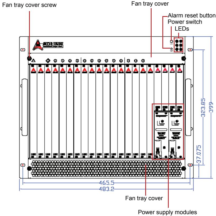
Figure 2-1: PXIS-3320 front view
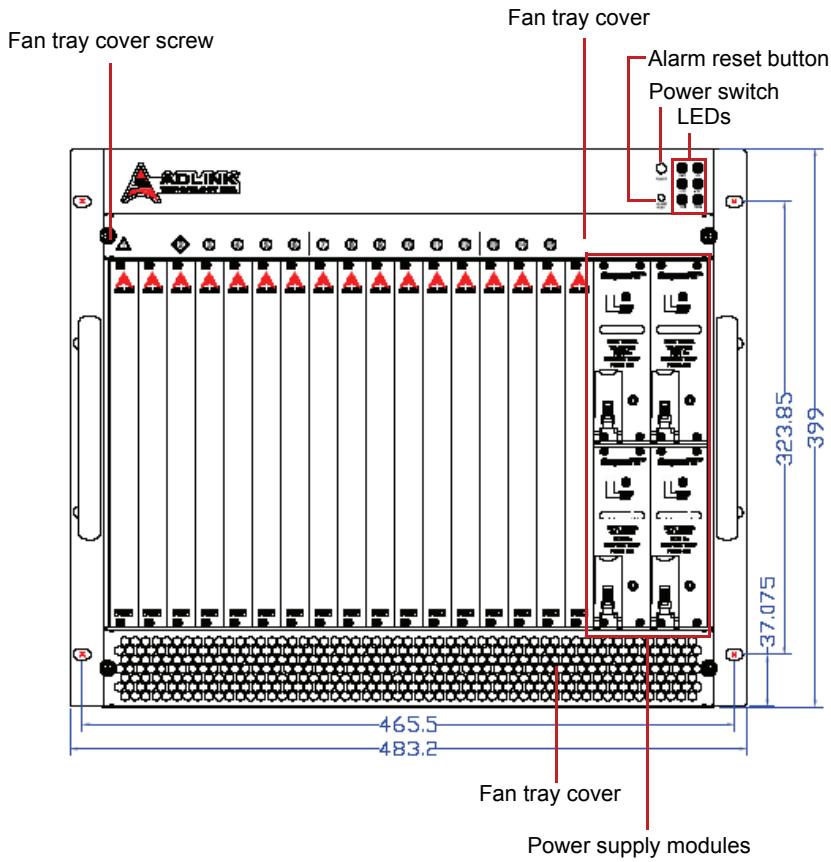
Figure 2-2: PXIS-3320/1000W front view
# 2.2 Right View
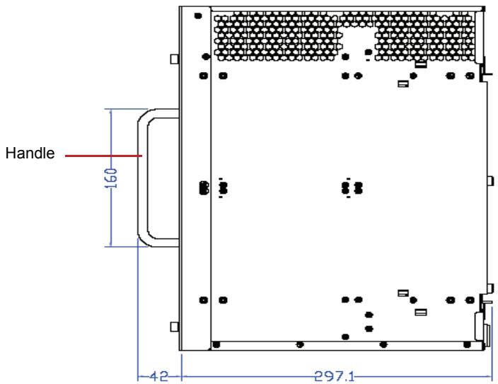
Figure 2-3: PXIS-3320 and PXIS/1000W right view
# 2.3 Top View
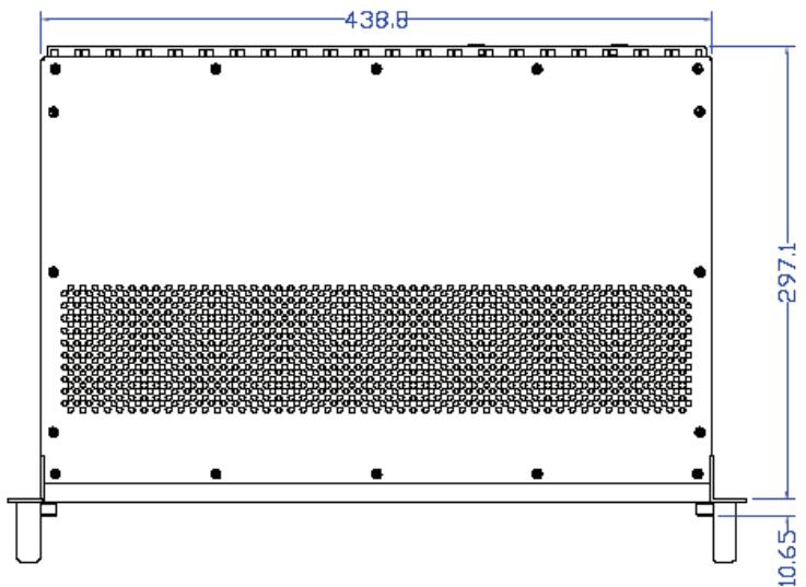
Figure 2-4: PXIS-3320 and PXIS/1000W top view
# 2.4 Rear View
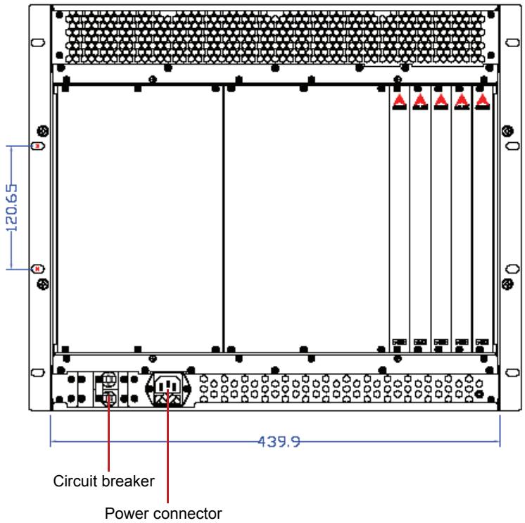
Figure 2-5: PXIS-3320 and PXIS-3320/1000W rear view
# 2.5 Backplane overview
The PXIS-3320 chassis comes with a 6U, 15-slot PXI backplane that supports one PXI system controller and 14 PXI/CompactPCI peripheral modules. This section illustrates the functions of the backplane.
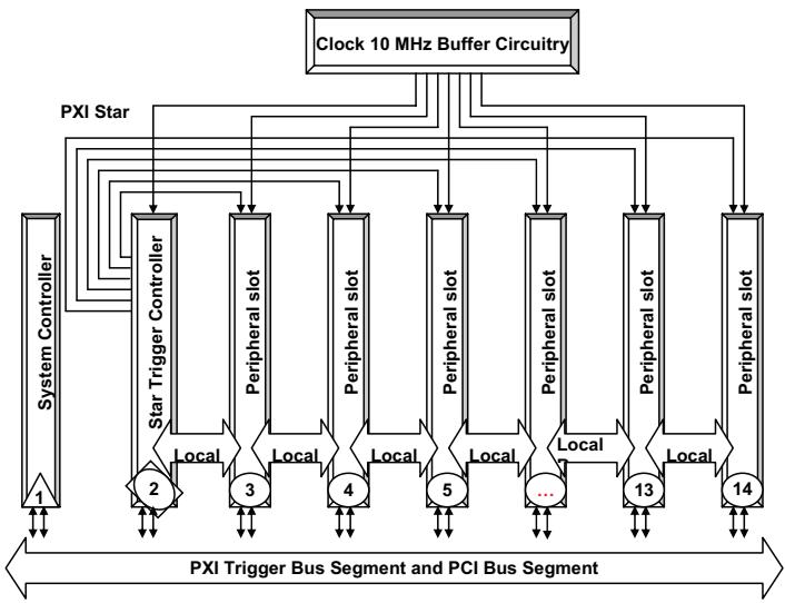
Figure 2-6: Backplane functions
# System Controller Slot
As defined by PXI specifications, the system controller slot occupies Slot 1 of the chassis. The system slot occupies two units of slot space and accommodates either a 1-slot or 2-slot 6U PXI/cPCI system controller. It is recommended that you use ADLINK cPCI-6840 and cPCI-6860A system controller for the PXIS-3320 chassis.
# Star Trigger Slot
Slot 2 is designated as the Star Trigger (ST) slot. This slot features a dedicated trigger line between itself and slots 3 to 15. The star trigger delivers trigger signals with ultra-low skew (<1ns) to peripheral modules. To use the star trigger functionality, you must install a special star trigger controller in Slot 2.
# Peripheral Slots
The PXIS-3320 chassis backplane accommodates up to fourteen 6U PXI/CompctPCI peripheral modules.
# Local Bus
The PXI backplane's local bus is a daisy-chained bus that connects each peripheral slot with the slots on its left and right. Each local bus is 14 lines wide and can pass analog and digital signals between modules or provide a high-speed, sideband communication path that does not affect the PCI bandwidth.
Following PXI specifications, the local bus connects all adjacent slots except Slots 1 and 2.
# Trigger Bus
The backplane's trigger bus is an 8-line bus that connects all slots in the same PCI segment. Users can use triggers to synchronize the operation of several PXI peripheral modules, or use one module to control accurate timing sequences of operations performed on other modules in the system. Modules can pass trigger signals or clock signals to other modules through the trigger bus, allowing precise timed responses to asynchronous external events that the system is monitoring or controlling.
# 10 MHz Reference Clock
The backplane supplies every peripheral slot with a 10 MHz system clock signal (PXI\_CLK10). An independent clock buffer (having source impedance matched to the backplane and a skew of <1ns between slots) drives the clock signals to each peripheral slot.
You can use this common reference clock signal to synchronize multiple modules in a measurement or control system or drive PXI\_CLK10 from an external source through the PXI\_CLK10\_IN pin on the P2 connector of the star trigger slot.
# 3 Installation
The chapter describes the procedures on how to install the system controller to the PXIS-3320 chassis. It also provides information on how to power up and monitor the system.
# 3.1 Calculating Power Consumption
Before installing any modules into the PXIS-3320 chassis, calculate the total system power requirement and check the power saving requirements for each DC power source including the +5 V, +3.3 V, +12 V, and -12 V supply rail. Refer to Appendix A for the maximum usable power.
# 3.2 Installing the Chassis and Starting Up
Follow the steps to power on the chassis.
1. For rackmount or bench-top installation, provide a sufficient space under the chassis for ventilation and make sure that the chassis is installed on a flat and stable surface.
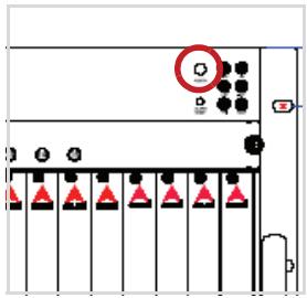
2. Put the power switch in the standby (OFF) position. The power switch protrudes from the bezel when the system is in standby power mode. Refer to the illustration below. The front-panel power switch turns the system ON or OFF.
3. Plug the AC power cord to a properly grounded wall socket or power strip.
4. Make sure that the CPU, memory modules, and storage device are properly installed on the system controller module.
5. Push down (loose) the ejector/injector handles of the system controller module.
6. Align the system controller module's top and bottom edges to the card guides.
7. Carefully slide the system controller module into the chassis, then push the ejector/injector handle up to secure the module in place. Secure the module with screws from the chassis front panel.
8. Install additional 6U PXI/CompactPCI peripheral modules, if needed.
9. Press the power switch. The amber LED and green LEDs on the upper right corner of the front panel light up. The chassis fans also start to rotate.
# NOTE
If the chassis fails to turn on, refer to Chapter 4: Troubleshooting and Preventive Maintenance for details.
# 3.3 Monitoring the System
Light Emitting Diodes (LEDs) on the front panel tell you the power status, chassis temperature, and fan operations. Refer to Table 3-1 for details.
<table>| LED | Function | Color | Status | Indication |
| Power | DC rail voltages (+3.3 V, +5 V, +12 V, -12 V) | Green | ON | Power is supplied to the system |
| OFF | No power is supplied to the system |
| Temperature | Internal temperature status | Red | ON | Internal temperature is less than 50°C |
| Flashing | internal temperature is more than 50°C |
| Fan | Fan speeds and operation | Amber | ON | Fan speed is normal |
| Flashing | Fan speed is abnormal; fan is defective |
Table 3-1: LED indications
# 3.4 Alarms
The chassis comes with an alarm buzzer and an alarm reset button. The alarm buzzer beeps to alert you of any power, temperature, or fan failure. The alarm reset button resets the alarm monitor system and stops the buzzer.
# 3.5 Grounding the Chassis
The backplane's mounting holes may be grounded in two ways. First, the mounting holes labeled as GND with circle soldering mask can be connected to the signal ground plane of the backplane. Second, the mounting holes labeled as FGND with square soldering mask can be connected to the power ground plane (the earth), and is isolated from the signal ground.
A proper signal and power wiring helps reduce the effects of ground loop and increases the accuracy of measurement.
By default, the PXIS-3320 backplane is mounted on the chassis through the FGND mounting holes. The signal ground (GND), therefore, is isolated to the power ground (FGND). For applications that require the short of signal ground and power ground, an external wiring is needed to connect the GND and FGND soldering pots.
# 3.6 Changing the Power Supply Modules
The PXIS-3320 chassis comes with two 3U CompactPCI power supply modules, while the PXIS-3320/1000W chassis comes with four 3U CompactPCI power supply modules. The power supply modules are current-sharing and are hot-swappable.
To replace the power modules:
1. Release the handle of the defective power module.
2. Push down the handle to eject the power module from the chassis.
3. Carefully pull the power module out from the chassis, then set aside.
4. Align the top and bottom edges of power supply modules to the card guides, then install the power supply module into the chassis.
5. Use the handle to firmly connect the power module into the chassis backplane.
# 3.7 Changing the Fans
The PXIS-3320 chassis has ten 80 mm x 80 mm x 25 mm fans. These fans are installed in two decks of fan trays. Five fans are located at the bottom of the chassis for air intake, while the other five fans are installed on top of the chassis for air ventilation. The fan trays are hot-swappable.
When a fan fails to operate, the alarm buzzer beeps and the fan LED flashes to alert you. Reset the alarm by pressing the alarm reset button, then replace the defective fan.
To replace a defective fan:
1. Remove the fan tray cover by loosening the thumb screw.
2. Check the LED in front of each fan tray. The LED blinks when the fan is defective.
3. Remove two screws that secure the fan tray to the chassis, then carefully pull the tray out of the chassis.
4. Install a new fan into the tray, then secure it with two screws you earlier removed.
5. Replace the fan tray cover.
# 4 Troubleshooting and Preventive Maintenance
# 4.1 Troubleshooting for Power Failure of PXIS-3320
When the PXI-3320 chassis fails to turn on, refer to Table 4-1 for basic power troubleshooting. The table lists the most common cause for power failure and the recommends process to correct the problem.
| Possible Causes | What to Do |
| The power cord is not connected to the power outlet. | Make sure that the power cord is connected to a properly grounded and live electrical outlet. Try connecting another electrical equipment to this outlet to make sure that it has power. |
| Power switch is not at ON position. | Set the power switch to the ON position. |
| The circuit breaker is not at ON position. | Make sure to turn off the power switch before setting the circuit breaker to ON position. After turning the circuit breaker on, turn the power switch on. |
| Power supply has failed. | Check the LED indicators on the CompactPCI power supply modules. If the POWER LED is off or the FAULT LED lights up orange when you press the power switch, the power supply module may be damaged. Contact an ADLINK representative for more information. |
Table 4-1: Troubleshooting Power Failures
# 4.2 Cleaning
It is recommended that you clean the interior and exterior of the PXIS-3320 chassis regularly. To clean individual CompactPCI or PXI modules, refer to the documentation that came with the module.
# NOTE
Always turn the chassis off and disconnect the power cord from the electrical socket before cleaning the chassis.
# Cleaning the Chassis Interior
Use a dry, low-velocity stream of air to clean the interior of the chassis. Clean around components with a soft-bristle brush. If you must use liquid for minor interior cleaning, use a 75% isopropyl alcohol solution, then rinse the area with de-ionized water.
# Cleaning the Chassis Exterior
Use a dry lint-free cloth or a soft-bristle brush to clean the exterior surfaces of the chassis. To remove dirt, moisten a cloth with a mild soap solution to wipe the exterior surfaces of the chassis. To remove any soap residue, wipe the surface with a cloth moistened with clean water. Do not use abrasive compounds to clean any part of the chassis.
# A Specifications
# A.1 General
Complies with PXI specifications and accepts modules compliant with CompactPCI, PICMG 2.0 specifications.
# A.2 Power Supply
▶ PICMG standards: PICMG 2.11-compliant
▶ Input voltage: 100 to 240 VAC
▶ Input frequency: 47 to 63 Hz
▶ Output: 250 W (each)
| VDC | Typical | Maximum |
| +5 V | 25.0 A | 33.0 A |
| +3.3 V | 18.0 A | 33.0 A |
| +12 V | 5.0 A | 5.5 A |
| -12 V | 0.5 A | 1 A |
# A.3 System Monitoring
System LEDs
| LED | Function/Setting | Status | Indication |
| Power | Voltage monitoring of +3.3 V, +5 V, +12 V, -12 V | ON | Power is supplied |
| Temperature | Temperature monitoring. 50°C (default setting) | ON | Temperature is normal |
| FLASHING | Temperature exceeds normal settings |
| Fan | Fan speed monitoring | ON | Normal fan speed |
| FLASHING | Fan is not working or has malfunctioned |
Buzzer/Alarm
| Alarm/ Buzzer | Function |
| Alarm buzzer | Beeps when any alarm occurs |
| Alarm reset button | Resets the alarm monitor system |
# A.4 Cooling System
Front-access hot-swappable fan trays for air intake and ventilation
▶ Type: 12 VDC brush-less, dual-ball bearing
▶ Five fans for air intake and five fans for ventilation
▶ Rated fan speed: 4000 to 5000 RPM
▶ Rated fan power: 2.64W
▶ Airflow for intake: 241 CFM
▶ Airflow for ventilation: 241 CFM
# A.5 Physical
▶ Number of slots: 15 (one system slot, 14 peripheral slots)
▶ Dimensions: 484 mm x 295 mm x 398 mm (L x W x H) without handles
▶ Weight: 23 kg
# A.6 Operating Environment
Ambient temperature range
| Model | Temperature |
| PXIS-3320 | 0 to 50°C |
| PXIS-3320/1000W | 0 to 50°C |
Relative humidity: 10 to 90%, non-condensing
# A.7 Backplane
▶ Backplane bare-board material: UL 94V-0 rated
▶ Backplane connectors: Conforms to IEC-917 and IEC 1076-4-101, UL 94V-0 rated
# A.8 Shock and Vibration
▶ Shock: 15 G peak-to-peak, 11 ms duration, non-operation
▶ Random Vibration
▶ Operating: 5 to 500 Hz, 0.5 GRMS each axis
▷ Nonoperating: 5 to 500 Hz, 1.88 GRMS each axis
# A.9 Safety and EMC/EMI Compliance
EMC/EMI: CE, FCC Class A
# B Backplane Drawing and Pin Assignments
# B.1 Backplane Layout
The following figures show the front and rear view of the PXIS-3320 backplane.
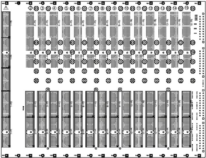
Figure B-1: CBX-6015 front view
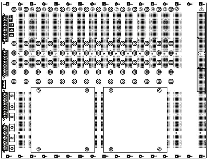
Figure B-2: CBX-6015 rear view
# B.2 Backplane CBX-6015 Connectors Pin Assignments
# PXI Connectors Pin Assignments
System Slot (Slot #1) P1 Pin Assignment
| Pin | Z | A | B | C | D | E | F |
| 25 | GND | +5V | REQ64# | ENUM# | +3.3V | +5V | GND |
| 24 | GND | AD[1] | +5V | V(I/O) | AD[0] | ACK64# | GND |
| 23 | GND | +3.3V | AD[4] | AD[3] | +5V | AD[2] | GND |
| 22 | GND | AD[7] | GND | +3.3V | AD[6] | AD[5] | GND |
| 21 | GND | +3.3V | AD[9] | AD[8] | GND | C/BE[0]# | GND |
| 20 | GND | AD[12] | GND | V(I/O) | AD[11] | AD[10] | GND |
| 19 | GND | +3.3V | AD[15] | AD[14] | GND | AD[13] | GND |
| 18 | GND | SERR# | GND | +3.3V | PAR | C/BE[1]# | GND |
| 17 | GND | +3.3V | IPMB_SCL | IPMB_SDA | GND | PERR# | GND |
| 16 | GND | DEVSEL# | GND | V(I/O) | STOP# | LOCK# | GND |
| 15 | GND | +3.3V | FRAME# | IRDY# | GND | TRDY# | GND |
| 12-14 | Key |
| 11 | GND | AD[18] | AD[17] | AD[16] | GND | C/BE[2]# | GND |
| 10 | GND | AD[21] | GND | +3.3V | AD[20] | AD[19] | GND |
| 9 | GND | C/BE[3]# | GND | AD[23] | GND | AD[22] | GND |
| 8 | GND | AD[26] | GND | V(I/O) | AD[25] | AD[24] | GND |
| 7 | GND | AD[30] | AD[29] | AD[28] | GND | AD[27] | GND |
| 6 | GND | REQ# (1) | GND | +3.3V | CLK (1) | AD[31] | GND |
| 5 | GND | BRSVP1A5 | BRSVP1B5 | PCIRST# | GND | GNT# (1) | GND |
| 4 | GND | IPMB_PWR | GND | V(I/O) | INTP | INTS | GND |
| 3 | GND | INTA# (1) | INTB# (1) | INTC# (1) | +5V | INTD# (1) | GND |
| 2 | GND | TCK | +5V | TMS | TDO | TDI | GND |
| 1 | GND | +5V | -12V | TRST# | +12V | +5V | GND |
| Pin | Z | A | B | C | D | E | F |
System Slot (Slot #1) P2 Pin Assignment
| Pin | Z | A | B | C | D | E | F |
| 22 | GND | PXI_BRSVA22 | PXI_BRSVB22 | PXI_BRSVC22 | PXI_BRSVD22 | PXI_BRSVE22 | GND |
| 21 | GND | CLK6 | GND | NC | NC | NC | GND |
| 20 | GND | CLK5 | GND | NC | GND | NC | GND |
| 19 | GND | GND | GND | SMBDATA | SMBCLK | SMBALERT- | GND |
| 18 | GND | PXI_TRIG3 | PXI_TRIG4 | PXI_TRIG5 | GND | PXI_TRIG6 | GND |
| 17 | GND | PXI_TRIG2 | GND | PRST# | REQ6# | GNT6# | GND |
| 16 | GND | PXI_TRIG1 | PXI_TRIG0 | DEG# | GND | PXI_TRIG7 | GND |
| 15 | GND | PXI_BRSVA15 | GND | FAL# | REQ5# | GNT5# | GND |
| 14 | GND | AD[35] | AD[34] | AD[33] | GND | AD[32] | GND |
| 13 | GND | AD[38] | GND | V(I/O) | AD[37] | AD[36] | GND |
| 12 | GND | AD[42] | AD[41] | AD[40] | GND | AD[39] | GND |
| 11 | GND | AD[45] | GND | V(I/O) | AD[44] | AD[43] | GND |
| 10 | GND | AD[49] | AD[48] | AD[47] | GND | AD[46] | GND |
| 9 | GND | AD[52] | GND | V(I/O) | AD[51] | AD[50] | GND |
| 8 | GND | AD[56] | AD[55] | AD[54] | GND | AD[53] | GND |
| 7 | GND | AD[59] | GND | V(I/O) | AD[58] | AD[57] | GND |
| 6 | GND | AD[63] | AD[62] | AD[61] | GND | AD[60] | GND |
| 5 | GND | C/BE[5]\# | GND | V(I/O) | C/BE[4]\# | PAR64 | GND |
| 4 | GND | V(I/O) | PXI_BRSVB4 | C/BE[7]\# | GND | C/BE[6]\# | GND |
| 3 | GND | CLK4 | GND | GNT3# | REQ4# | GNT4# | GND |
| 2 | GND | CLK2 | CLK3 | GND (SYS\#) | GNT2# | REQ3# | GND |
| 1 | GND | CLK1 | GND | REQ1# | GNT1# | REQ2# | GND |
| Pin | Z | A | B | C | D | E | F |
Star Trigger Slot (Slot #2) P1 Pin Assignment
| Pin | Z | A | B | C | D | E | F |
| 25 | GND | +5V | REQ64# | ENUM# | +3.3V | +5V | GND |
| 24 | GND | AD[1] | +5V | V(I/O) | AD[0] | ACK64# | GND |
| 23 | GND | +3.3V | AD[4] | AD[3] | +5V | AD[2] | GND |
| 22 | GND | AD[7] | GND | +3.3V | AD[6] | AD[5] | GND |
| 21 | GND | +3.3V | AD[9] | AD[8] | M66EN | C/BE[0]# | GND |
| 20 | GND | AD[12] | GND | V(I/O) | AD[11] | AD[10] | GND |
| 19 | GND | +3.3V | AD[15] | AD[14] | GND | AD[13] | GND |
| 18 | GND | SERR# | GND | +3.3V | PAR | C/BE[1]# | GND |
| 17 | GND | +3.3V | IPMB_SCL | IPMB_SDA | GND | PERR# | GND |
| 16 | GND | DEVSEL# | GND | V(I/O) | STOP# | LOCK# | GND |
| 15 | GND | +3.3V | FRAME# | IRDY# | GND | TRDY# | GND |
| 12-14 | Key | | | | | | |
| 11 | GND | AD[18] | AD[17] | AD[16] | GND | C/BE[2]# | GND |
| 10 | GND | AD[21] | GND | +3.3V | AD[20] | AD[19] | GND |
| 9 | GND | C/BE[3]# | IDSEL (1) | AD[23] | GND | AD[22] | GND |
| 8 | GND | AD[26] | GND | V(I/O) | AD[25] | AD[24] | GND |
| 7 | GND | AD[30] | AD[29] | AD[28] | GND | AD[27] | GND |
| 6 | GND | REQ# (1) | GND | +3.3V | CLK (1) | AD[31] | GND |
| 5 | GND | BRSVP1A5 | BRSVP1B5 | PCIRST# | GND | GNT# (1) | GND |
| 4 | GND | IPMB_PWR | GND | V(I/O) | INTP | INTS | GND |
| 3 | GND | INTA# (1) | INTB# (1) | INTC# (1) | +5V | INTD# (1) | GND |
| 2 | GND | TCK | +5V | TMS | TDO | TDI | GND |
| 1 | GND | +5V | -12V | TRST# | +12V | +5V | GND |
| Pin | Z | A | B | C | D | E | F |
Star Trigger Slot (Slot #2) P2 Pin Assignment
| Pin | Z | A | B | C | D | E | F |
| 22 | GND | PXI_BRSVA22 | PXI_BRSVB22 | PXI_BRSVC22 | PXI_BRSVD22 | PXI_BRSVE22 | GND |
| 21 | GND | PXI_LBR0 | GND | PXI_LBR1 | PXI_LBR2 | PXI_LBR3 | GND |
| 20 | GND | PXI_LBR4 | PXI_LBR5 | PXI_STAR0 (2) | GND | PXI_STAR1 (2) | GND |
| 19 | GND | PXI_STAR2 (2) | GND | PXI_STAR3 (2) | PXI_STAR4 | PXI_STAR5 | GND |
| 18 | GND | PXI_TRIG3 | PXI_TRIG4 | PXI_TRIG5 | GND | PXI_TRIG6 | GND |
| 17 | GND | PXI_TRIG2 | GND | N/C | PXI_CLK10_IN | PXI_CLK10 | GND |
| 16 | GND | PXI_TRIG1 | PXI_TRIG0 | N/C | GND | PXI_TRIG7 | GND |
| 15 | GND | PXI_BRSVA15 | GND | N/C | PXI_STAR6 | PXI_LBR6 | GND |
| 14 | GND | AD[35] | AD[34] | AD[33] | GND | AD[32] | GND |
| 13 | GND | AD[38] | GND | V(I/O) | AD[37] | AD[36] | GND |
| 12 | GND | AD[42] | AD[41] | AD[40] | GND | AD[39] | GND |
| 11 | GND | AD[45] | GND | V(I/O) | AD[44] | AD[43] | GND |
| 10 | GND | AD[49] | AD[48] | AD[47] | GND | AD[46] | GND |
| 9 | GND | AD[52] | GND | V(I/O) | AD[51] | AD[50] | GND |
| 8 | GND | AD[56] | AD[55] | AD[54] | GND | AD[53] | GND |
| 7 | GND | AD[59] | GND | V(I/O) | AD[58] | AD[57] | GND |
| 6 | GND | AD[63] | AD[62] | AD[61] | GND | AD[60] | GND |
| 5 | GND | C/BE[5]\# | GND | V(I/O) | C/BE[4]\# | PAR64 | GND |
| 4 | GND | V(I/O) | PXI_BRSVB4 | C/BE[7]\# | GND | C/BE[6]\# | GND |
| 3 | GND | PXI_LBR7 | GND | PXI_LBR8 | PXI_LBR9 | PXI_LBR10 | GND |
| 2 | GND | PXI_LBR11 | PXI_LBR12 | N.C (SYS#) | PXI_STAR7 | PXI_STAR8 | GND |
| 1 | GND | PXI_STAR9 | GND | PXI_STAR10 | PXI_STAR11 | PXI_STAR12 | GND |
| Pin | Z | A | B | C | D | E | F |
General Peripheral Slot (Slot #3\~#15) P1 Pin Assignment
| Pin | Z | A | B | C | D | E | F |
| 25 | GND | +5V | REQ64# | ENUM# | +3.3V | +5V | GND |
| 24 | GND | AD[1] | +5V | V(I/O) | AD[0] | ACK64# | GND |
| 23 | GND | +3.3V | AD[4] | AD[3] | +5V | AD[2] | GND |
| 22 | GND | AD[7] | GND | +3.3V | AD[6] | AD[5] | GND |
| 21 | GND | +3.3V | AD[9] | AD[8] | M66EN | C/BE[0]# | GND |
| 20 | GND | AD[12] | GND | V(I/O) | AD[11] | AD[10] | GND |
| 19 | GND | +3.3V | AD[15] | AD[14] | GND | AD[13] | GND |
| 18 | GND | SERR# | GND | +3.3V | PAR | C/BE[1]# | GND |
| 17 | GND | +3.3V | IPMB_SCL | IPMB_SDA | GND | PERR# | GND |
| 16 | GND | DEVSEL# | GND | V(I/O) | STOP# | LOCK# | GND |
| 15 | GND | +3.3V | FRAME# | IRDY# | GND | TRDY# | GND |
| 12-14 | Key | | | | | | |
| 11 | GND | AD[18] | AD[17] | AD[16] | GND | C/BE[2]# | GND |
| 10 | GND | AD[21] | GND | +3.3V | AD[20] | AD[19] | GND |
| 9 | GND | C/BE[3]# | IDSEL (1) | AD[23] | GND | AD[22] | GND |
| 8 | GND | AD[26] | GND | V(I/O) | AD[25] | AD[24] | GND |
| 7 | GND | AD[30] | AD[29] | AD[28] | GND | AD[27] | GND |
| 6 | GND | REQ# (1) | GND | +3.3V | CLK (1) | AD[31] | GND |
| 5 | GND | BRSVP1A5 | BRSVP1B5 | PCIRST# | GND | GNT# (1) | GND |
| 4 | GND | IPMB_PWR | GND | V(I/O) | INTP | INTS | GND |
| 3 | GND | INTA# (1) | INTB# (1) | INTC# (1) | +5V | INTD# (1) | GND |
| 2 | GND | TCK | +5V | TMS | TDO | TDI | GND |
| 1 | GND | +5V | -12V | TRST# | +12V | +5V | GND |
| Pin | Z | A | B | C | D | E | F |
General Peripheral Slot (Slot #3\~#15) P2 Pin Assignment
| Pin | Z | A | B | C | D | E | F |
| 22 | GND | PXI_BRSVA22 | PXI_BRSVB22 | PXI_BRSVC22 | PXI_BRSVD22 | PXI_BRSVE22 | GND |
| 21 | GND | PXI_LBR0 | GND | PXI_LBR1 | PXI_LBR2 | PXI_LBR3 | GND |
| 20 | GND | PXI_LBR4 | PXI_LBR5 | PXI_LBL0 | GND | PXI_LBL1 | GND |
| 19 | GND | PXI_LBL2 | GND | PXI_LBL3 | PXI_LBL4 | PXI_LBL5 | GND |
| 18 | GND | PXI_TRIG3 | PXI_TRIG4 | PXI_TRIG5 | GND | PXI_TRIG6 | GND |
| 17 | GND | PXI_TRIG2 | GND | N/C | PXI_STAR (2) | PXI_CLK10 | GND |
| 16 | GND | PXI_TRIG1 | PXI_TRIG0 | N/C | GND | PXI_TRIG7 | GND |
| 15 | GND | PXI_BRSVA15 | GND | N/C | PXI_LBL6 | PXI_LBR6 | GND |
| 14 | GND | AD[35] | AD[34] | AD[33] | GND | AD[32] | GND |
| 13 | GND | AD[38] | GND | V(I/O) | AD[37] | AD[36] | GND |
| 12 | GND | AD[42] | AD[41] | AD[40] | GND | AD[39] | GND |
| 11 | GND | AD[45] | GND | V(I/O) | AD[44] | AD[43] | GND |
| 10 | GND | AD[49] | AD[48] | AD[47] | GND | AD[46] | GND |
| 9 | GND | AD[52] | GND | V(I/O) | AD[51] | AD[50] | GND |
| 8 | GND | AD[56] | AD[55] | AD[54] | GND | AD[53] | GND |
| 7 | GND | AD[59] | GND | V(I/O) | AD[58] | AD[57] | GND |
| 6 | GND | AD[63] | AD[62] | AD[61] | GND | AD[60] | GND |
| 5 | GND | C/BE[5]\# | GND | V(I/O) | C/BE[4]\# | PAR64 | GND |
| 4 | GND | V(I/O) | PXI_BRSVB4 | C/BE[7]\# | GND | C/BE[6]\# | GND |
| 3 | GND | PXI_LBR7 | GND | PXI_LBR8 | PXI_LBR9 | PXI_LBR10 | GND |
| 2 | GND | PXI_LBR11 | PXI_LBR12 | N/C (SYS#) | PXI_LBL7 | PXI_LBL8 | GND |
| 1 | GND | PXI_LBL9 | GND | PXI_LBL10 | PXI_LBL11 | PXI_LBL12 | GND |
| Pin | Z | A | B | C | D | E | F |
B.3 Bus Segments and Interrupt Routings
| Bus | Slot # | IDSEL | REQ#/GNT# | PCICLK | PXI P1Pin A3 | PXI P1Pin B3 | PXI P1Pin C3 | PXI P1Pin E3 |
| BUS #1 | Slot 1 (SYS) | - | - | - | INTA# | INTB# | INTC# | INTD# |
| Slot 2 | AD30 | 1 | 5 | INTC# | INTD# | INTA# | INTB# |
| Slot 3 | AD29 | 2 | 1 | INTB# | INTC# | INTD# | INTA# |
| Slot 4 | AD28 | 3 | 3 | INTA# | INTB# | INTC# | INTD# |
| Slot 5 | AD27 | 4 | 4 | INTD# | INTA# | INTB# | INTC# |
| Slot 6 | AD26 | 5 | 0 | INTC# | INTD# | INTA# | INTB# |
| B1 | Bridge1 | AD31 | 0 | 2 | INTD# | INTA# | INTB# | INTC# |
| BUS #2 | Slot 7 | S1_AD30 | S1_1 | S1_1 | INTB# | INTC# | INTD# | INTA# |
| Slot 8 | S1_AD29 | S1_2 | S1_2 | INTA# | INTB# | INTC# | INTD# |
| Slot 9 | S1_AD28 | S1_3 | S1_3 | INTD# | INTA# | INTB# | INTC# |
| Slot 10 | S1_AD27 | S1_4 | S1_4 | INTC# | INTD# | INTA# | INTB# |
| Slot 11 | S1_AD26 | S1_5 | S1_5 | INTB# | INTC# | INTD# | INTA# |
| Slot 12 | S1_AD25 | S1_6 | S1_6 | INTA# | INTB# | INTC# | INTD# |
| B2 | Bridge2 | S1_AD31 | S1_0 | S1_0 | INTC# | INTD# | INTA# | INTB# |
| BUS #3 | Slot 13 | S2_AD31 | S2_0 | S2_0 | INTB# | INTC# | INTD# | INTA# |
| Slot 14 | S2_AD30 | S2_1 | S2_1 | INTA# | INTB# | INTC# | INTD# |
| Slot 15 | S2_AD29 | S2_2 | S2_2 | INTD# | INTA# | INTB# | INTC# |
# B.4 Bus Segments and Interrupt Routings
| Physical Slot Number | PXI_STAR (P2-D17) |
| Slot 2(Star Trigger Slot) | PXI_STAR0 ~ PXI_STAR12 |
| Slot 3 | PXI_STAR0 |
| Slot 4 | PXI_STAR1 |
| Slot 5 | PXI_STAR2 |
| Slot 6 | PXI_STAR3 |
| Slot 7 | PXI_STAR4 |
| Slot 8 | PXI_STAR5 |
| Slot 9 | PXI_STAR6 |
| Slot 10 | PXI_STAR7 |
| Slot 11 | PXI_STAR8 |
| Slot 12 | PXI_STAR9 |
| Slot 13 | PXI_STAR10 |
| Slot 14 | PXI_STAR11 |
| Slot 15 | PXI_STAR12 |
# B.5 Miscellaneous Connectors Pin Assignments
CN1, CN7, CN8, CN9: ATX-like DC Power input connectors
| Signal Name | Pin # | Pin # | Signal Name |
| V2SENSE | 1 | 11 | V2 (+3.3V) |
| V2 (+3.3V) | 2 | 12 | V4 (-12V) |
| GND | 3 | 13 | GND |
| V1 (+5V) | 4 | 14 | INH# |
| GND | 5 | 15 | GND |
| V1 (+5V) | 6 | 16 | SRTN |
| GND | 7 | 17 | GND |
| FAL#1 | 8* | 18* | V3(+12V)SENSE |
| DEG#1 | 9* | 19 | V1(+5V) SENSE |
# NOTE
Pin #8, #9, and #18 are not standard ATX power definitions.
# PCI VIO Selection Screw Terminals
| Position | Signal Name |
| J1 | +5V |
| J3 | V(I/O) |
| J4 | +3.3V |
| J7 | GND |
| J10 | -12V |
| J11 | +12V |
# NOTE
The V(I/O) must be shorted to either +3.3V or +5V. The default factory setting is to short V(I/O) to +5V.J1 INH#: DC power inhibit signa.
# J6 INH#: DC power inhibit signal
| J6<img src="images/bc2405846589bae02258d54ffba741f45f2cf7e232b2662693260c6177db226b.jpg"/> | Pin # | Signal Name |
| 1 | INH# |
| 2 | GND |
# J8 RST#: System reset signal
| J8<img src="images/5f9cd681daf36a18aa6d71d2459f3ef7dd53575deb477d6fec2da2fefa493240.jpg"/> | Pin # | Signal Name |
| 1 | RST# |
| 2 | GND |
# J9 FAL#: Power supply fail input
| J9<img src="images/61a61064b16a62f737e210dd6921d9ce311a7dcf6630a6ee0ba8b3d5b11b06ca.jpg"/> | Pin # | Signal Name |
| 1 | FAL# |
| 2 | GND |
# J5: Connector for LED power status
| J5 | Name | Pin # | Pin # | Name |
| GND | 8 | 7 | +3.3V |
| GND | 6 | 5 | +5V |
| GND | 4 | 3 | -12V |
| GND | 2 | 1 | +12V |
# CN5: SMB (System Management Bus) connector
| CN2(a) vs. | Pin # | Name |
| 1 | IPMB_CLK |
| 2 | GND |
| 3 | IPMB_DATA |
| 4 | IPMB_PWR |
| 5 | ALERT |
# NOTE
The SMB is connected to the P2 of the system slot.
# JP1: 10 MHz Reference Clock
| Pin # | Description |
| (c2c2e1) | Pin 1-2(Default) | Internal 10MHz system clock PXI_CLK10 |
| (f2e2) | Pin 2-3 | External clock through the PXI_CLK10_IN on star trigger slot |
# J2: POWER SENSE
| J2<img src="images/5d93c4c025d9f25ba28795fbaf181cc9ced207d49153ba74e1e1d8b4fcb8a975.jpg"/> | Pin # | Name |
| 1 | NC |
| 2 | +12V |
| 3 | +3.3V |
| 4 | GND |
| 5 | +5V |
# Important Safety Instructions
Read and follow all instructions marked on the product and in the documentation before operating the system. Retain all safety and operating instructions for future use.
▶ Read these safety instructions carefully.
- Keep this user’s manual for future reference.
The equipment should be operated in an ambient temperature between $0^{\circ}$ C to $50^{\circ}$ C.
The equipment should be operated only from the type of power source indicated on the rating label. Make sure the voltage of the power source is correct when connecting the equipment to the power outlet.
If the user's equipment has a voltage selector switch, make sure that the switch is set to the proper position for the area. The voltage selector switch is set at the factory to the correct voltage.
▶ For pluggable equipment, ensure they are installed near a socket-outlet that is easily accessible.
- Secure the power cord to prevent unnecessary accidents. Do not place anything over the power cord.
▶ If the equipment will not be in use for long periods of time, disconnect the equipment from the power outlet to avoid being damaged by transient overvoltage.
▶ All cautions and warnings on the equipment must be noted.
▶ Keep this equipment away from humidity.
▶ Do not use this equipment near water or a heat source.
▶ Place this equipment on a stable surface when installing to prevent injury.
▶ Never pour any liquid into the product to prevent fire or electrical shock.
▶ Openings in the chassis are provided for ventilation. Do not block or cover these openings. Make sure there is adequate space around the system for ventilation when setting up the work area. Never insert objects of any kind into the ventilation holes.
▶ To avoid electrical shock, always unplug all power and modem cables from wall outlets before removing the system covers.
▶ A Lithium-type battery is provided for the real time clock.
# CAUTION - Risk of explosion if battery is replaced by an incorrect type. Dispose used batteries as instructed.
▶ The equipment must be serviced by authorized technicians when:
The power cord or plug is damaged.
▷ Liquid has penetrated the equipment.
▷ It has been exposed to moisture.
$\triangleright$ It is not functioning or does not function according to the user's manual.
▷ It has been dropped and damaged.
▷ It has an obvious sign of breakage.
▶ Never attempt to fix the equipment. For safety reasons, the equipment should only be serviced by qualified personnel.
# Warranty Policy
Thank you for choosing ADLINK. To understand your rights and enjoy all the after-sales services we offer, please read the following carefully.
1. Before using ADLINK's products please read the user manual and follow the instructions exactly. When sending in damaged products for repair, please attach an RMA application form which can be downloaded from: http://rma.adlinktech.com/policy/home.htm/.
2. All ADLINK products come with a limited two-year guarantee, one year for products bought in China:
The warranty period starts on the day the product is shipped from ADLINK's factory.
▶ Peripherals and third-party products not manufactured by ADLINK will be covered by the original manufacturers' warranty.
For products containing storage devices (hard drives, flash cards, etc.), please back up your data before sending them for repair. ADLINK is not responsible for loss of data.
▶ Please ensure the use of properly licensed software with our systems. ADLINK does not condone the use of pirated software and will not service systems using such software. ADLINK will not be held legally responsible for products shipped with unlicensed software installed by the user.
For general repairs, please do not include peripheral accessories. If peripherals need to be included, be certain to specify which items you sent on the RMA Request & Confirmation Form. ADLINK is not responsible for items not listed on the RMA Request & Confirmation Form.
3. Our repair service is not covered by ADLINK's guarantee in the following situations:
▶ Damage caused by not following instructions in the User's Manual.
▶ Damage caused by carelessness on the user's part during product transportation.
▶ Damage caused by fire, earthquakes, floods, lightening, pollution, other acts of God, and/or incorrect usage of voltage transformers.
▶ Damage caused by unsuitable storage environments (i.e. high temperatures, high humidity, or volatile chemicals).
▶ Damage caused by leakage of battery fluid during or after change of batteries by customer/user.
▶ Damage from improper repair by unauthorized ADLINK technicians.
▶ Products with altered and/or damaged serial numbers are not entitled to our service.
▶ This warranty is not transferable or extendible.
▶ Other categories not protected under our warranty.
4. Customers are responsible for shipping costs to transport damaged products to ADLINK.
If you have any further questions, please email our FAE staff: service@adlinktech.com.