# SP2-EHL Series

# User’s Manual

Open-Frame Panel PC

![Exploded view of a computer monitor showing internal circuit board and fan components (no text or symbols)](.sp2-ehl-50m-p1400-1010-11/38670e3f1e9a51344ba0746e355eb0dab26681aa81b886f473196abc5cd236ca.jpg)

Manual Rev.: Rev. 1.1

Revision Date: March 05, 2025

Part Number: 50M-31131-1010

# Revision History

<table><tr><td>Revision</td><td>Description</td><td>Date</td></tr><tr><td>1.0</td><td>Initial release</td><td>2023-10-16</td></tr><tr><td>1.1</td><td>System layout updated</td><td>2025-03-05</td></tr></table>

# Preface

# Copyright

Copyright 2025 ADLINK Technology, Inc. This document contains proprietary information protected by copyright. All rights are reserved. No part of this manual may be reproduced by any mechanical, electronic, or other means in any form without prior written permission of the manufacturer.

# Disclaimer

The information in this document is subject to change without prior notice in order to improve reliability, design, and function and does not represent a commitment on the part of the manufacturer. In no event will the manufacturer be liable for direct, indirect, special, incidental, or consequential damages arising out of the use or inability to use the product or documentation, even if advised of the possibility of such damages.

# Environmental Responsibility

ADLINK is committed to fulfill its social responsibility to global environmental preservation through compliance with the European Union's Restriction of Hazardous Substances (RoHS) directive and Waste Electrical and Electronic Equipment (WEEE) directive. Environmental protection is a top priority for ADLINK. We have enforced measures to ensure that our products, manufacturing processes, components, and raw materials have as little impact on the environment as possible. When products are at their end of life, our customers are encouraged to dispose of them in accordance with the product disposal and/or recovery programs prescribed by their nation or company.

![Symbol of a trash bin crossed with a diagonal line and a horizontal bar below (no text or labels)](.sp2-ehl-50m-p1400-1010-11/8eac306f6b4bd3c2a34b6e7942dd371c1d4898fb941cec333b9c626e365b3df2.jpg)

Battery Labels (for products with battery)

![Symbol of a trash bin crossed out by two diagonal lines (no text or labels)](.sp2-ehl-50m-p1400-1010-11/368e0b67c8513ada67894954f4f9cfd9b195763d4edc02626c9094b4dccfcca1.jpg)

![Li-ion](.sp2-ehl-50m-p1400-1010-11/063d153b7f6714a97f1ddbb9013e66598716b966083f29cbedd9da593b32cd91.jpg)

![RECYCLE\nRBRC\nLi-ion\n7.800.822.8837](.sp2-ehl-50m-p1400-1010-11/7a859ad3c269f09240fdad5015793927656c4029e119860104e4fc9119db2811.jpg)

![廢電池請回收](.sp2-ehl-50m-p1400-1010-11/cebf0e5d484a6686d7739e7bd9502a9a9ef2b57d8068575182f53a483ef89242.jpg)

# California Proposition 65 Warning

![A yellow triangle with a thick black border containing a centered black exclamation point.](.sp2-ehl-50m-p1400-1010-11/157766f9624dd5ec7f5ea049592300d79d3f4ac16a613fcd8b34f63e21da0ba0.jpg)

WARNING: This product can expose you to chemicals including acrylamide, arsenic, benzene, cadmium, Tris(1,3-dichloro-2-propyl)phosphate (TDCPP), 1,4-Dioxane, formaldehyde, lead, DEHP, styrene, DINP, BBP, PVC, and vinyl materials, which are known to the State of California to cause cancer, and acrylamide, benzene, cadmium, lead, mercury, phthalates, toluene, DEHP, DIDP, DnHP,

DBP, BBP, PVC, and vinyl materials, which are known to the State of California to cause birth defects or other reproductive harm. For more information go to www.P65Warnings.ca.gov.

# Trademarks

Product names mentioned herein are used for identification purposes only and may be trademarks and/or registered trademarks of their respective companies.

# Conventions

Take note of the following conventions used throughout this manual to make sure that users perform certain tasks and instructions properly.

![The image displays a white document icon with a folded top-left corner. Faint horizontal lines run across the page, resembling text or a form. A large, bold red checkmark is overlaid on the left side of the document.](.sp2-ehl-50m-p1400-1010-11/c4df150eb313f1f307b422acbab15c5acf910395258af27a02bac77bb14e8954.jpg)
NOTE:

Additional information, aids, and tips that help users perform tasks.

![The image displays a yellow triangular warning sign with a black border. Inside the triangle is a large black exclamation point centered vertically and horizontally.](.sp2-ehl-50m-p1400-1010-11/ad45b3265b8952f0120b7fdbbff6d35dc8a6973ca23010486bca3cf937a130c3.jpg)
CAUTION:

Information to prevent minor physical injury, component damage, data loss, and/or program corruption when trying to complete a task.

![The image shows a standard warning symbol consisting of a dark red, upright triangle. Inside the triangle is a white exclamation point. Thin black vertical lines appear along the far left and right edges of the image.](.sp2-ehl-50m-p1400-1010-11/65b7a6f66ac69f2c3d4588890d9ec79b5b8306fe50e1b30f386e7bebc702bd62.jpg)
WARNING:

Information to prevent serious physical injury, component damage, data loss, and/or program corruption when trying to complete a specific task.

# Table of Contents

# Preface...

# List of Figures .... .vii

# List of Tables...... ..vii

# 1 Introduction....

1.1 Overview.. .9
1.2 Features.. .9
1.3 Package Contents. .9
1.4 Optional Accessories ... .9

# 2 Specifications .... .11

2.1 Product Specifications... .11
2.2 Functional Block Diagram . ..13

# 3 Mechanical Layout .. .15

3.1 SP2-7WP Dimensions... .15
3.2 Thermal Options . ..18

# 4 Getting Started....... .21

4.1 Adding or Changing Memory.. .21
4.2 Installing a Wi-Fi-Module.. .22
4.3 Mounting. .23

# 5 System Layout ......... .29

5.1 External I/O Connectors.. ..29
5.2 Internal I/O Connectors.. .29

# 6 Connector Pinouts and Jumper Settings .... ..33

6.1 Power Connector ... ..33
6.2 SATA Power Connector.. .33
6.3 SATA Data Connector... ..33
6.4 Resistive Touch Connector .. ..33
6.5 Capacitative Touch Connector. .34
6.6 Mini PCIe Connector.. .34
6.7 M.2 2230, E Key for Wi-Fi/Bluetooth Modules.. .35
6.8 Function Module Board Connector.. .36
6.9 LVDS/eDP Connector .. ..37
6.10 Power/Reset/LED Button .. ..38
6.11 Buzzer Connector . ..38
6.12 Mic In/Line Out Connector . .38

6.13 Speaker Connector .. ..39

6.14 Camera Connector... ..39

6.15 USB 2.0 Connector .. ..39

6.16 Volume & Backlight Control Connector .. ..39

6.17 Key Connector . ...40

6.18 Fan Connector . ..40

6.19 Clear CMOS Jumper.. ..40

6.20 LAN2 Connector . ..41

6.21 COM2 Connector.. ..41

6.22 COM1 Connector.. ..41

6.23 LED Connector .. ..42

6.24 I2 C Connector-1 . ..42

6.25 I2 C Connector-2 . ..42

6.26 RTC Battery Connector... ..42

6.27 DB40 Connector . ..43

6.28 GPIO Connector . ..43

6.29 UPS Connector.. ..45

6.30 M.2 M Key Connector .. ..45

# 7 BIOS Settings..... .47

7.1 BIOS Setup Menu... ..47

7.2 ADLINK Unique Settings.... ...48

# 8 Driver Installation .. .49

8.1 Driver Installation Steps . ..49

# Safety Instructions.... .51

# Getting Services.......... .53

# List of Figures

Figure 1: Functional block diagram.. ..13

Figure 2: SP2-7WP dimensions.. .15

Figure 3: SP2-10WP dimensions.. ..16

Figure 4: SP2-15WP dimensions.. .17

Figure 5: SP2-21WP dimensions.. .17

Figure 6: Active Cooling Heatsink.. .18

Figure 7: Heatsink dimensions . ..19

Figure 8: Cable routing considerations for heatsinks... .20

Figure 9: SP2-7WP cutout dimensions.. .24

Figure 10: SP2-10WP cutout dimensions.. .24

Figure 11: Mounting clip dimensions . .26

Figure 12: External I/O connectors .. .29

Figure 13: Mainboard connectors (Top) . ..30

Figure 14: Mainboard connectors (Bottom) .30

Figure 15: Digital input circuit .. .44

Figure 16: Digital output circuit .. .45

# List of Tables

Table 1: Heatsink components . .18

Table 2: External I/O legend.. .29

Table 3: Mainboard connector legend . .31

Table 4: GPIO connector pin voltage. .44

This page intentionally left blank.

# 1 Introduction

# 1.1 Overview

The SP2-EHL Series open-frame panel PC is based on the ultra- low-power Intel Atom® x6000E series processors (formerly Elkhart Lake) featuring flexible IO options. The SP2-EHL Series features efficient capabilities and compact size that are easy to integrate with kiosk and panel PC applications.

# 1.2 Features

• High power efficiency with Intel Atom® x6000E series processors (formerly Elkhart Lake)
• Extensive I/O and function expansion through wire-to-board connectors and custom function modules
• Comprehensive expansion and customization options for fast and easy integration with all form factors, kiosks, and all-in-one panel PC applications
• Enhanced protection in case of sudden power outage with support for back-up battery (Optional)
• Pre-compliance EMC testing and high ESD tolerance
• High reliability in case of power fluctuation with an optional 9-36V DC voltage range
• Simple cabling with optional 60W Power Over Ethernet module
• Supports up to 3 displays, including integrated panel, DisplayPort, and USB Type-C (Optional)

# 1.3 Package Contents

Before unpacking, check the shipping carton for any damage. If the shipping carton and/or contents are damaged, inform your dealer immediately. Retain the shipping carton and packing materials for inspection. Obtain authorization from your dealer before returning any product to ADLINK. Ensure that the following items are included in the package.

1x SP2-EHL Series Smart Panel

# 1.4 Optional Accessories

Panel-mount clip kit
• VESA kit
• Rear cover
• Active sink
Wi-Fi module
60W (12V/5A) or 84W (12V/7A) power supply
• Power cable (SP2-EHL to power supply)
. Cables for internal IO expansion
• Function Modules
. SP FM
. Titan FM
USB FM

![The image shows an icon of a document or piece of paper with a folded top-left corner. It has faint horizontal lines resembling text and features a large, bold red checkmark drawn over it.](.sp2-ehl-50m-p1400-1010-11/1e4e62a268e47ddd497a3be0530b5583a16f3f6385b0a23951b6028ede4ef1b6.jpg)
NOTE:

The contents of non-standard cPCI-3630 configurations may vary depending on the customer’s requirements.

This page intentionally left blank.

# 2 Specifications

2.1 Product Specifications

<table><tr><td>Model</td><td>SP2-07WP-EHL</td><td>SP2-10WP-EHL</td><td>SP2-15WP-EHL</td><td>SP2-21WP-EHL</td></tr><tr><td>Processor</td><td colspan="4">Intel Atom® x6425E, 2.0(3.0) GHz, 12W, 4C/32EU Intel Atom® x6413E, 1.5(3.0) GHz, 9W, 4C/16EU Intel Atom® x6211E, 1.2(3.0) GHz, 6W, 2C/16EU Intel Atom® J6412, 2.0(2.6) GHz, 10W, 4C/16EU</td></tr><tr><td>Memory</td><td colspan="4">1x SODIMM socket, DDR4 3200MHz (Up to 32GB)</td></tr><tr><td>Storage</td><td colspan="4">1x M.2 SATA M key 2280, support SATA SSD and NVME (PCIe x2) 1x 2.5" SSD/HDD SATA 6 Gbps port</td></tr><tr><td colspan="5">Display and Touch</td></tr><tr><td>Size</td><td>7"</td><td>10.1"</td><td>15.6"</td><td>21.5"</td></tr><tr><td>Resolution</td><td>1024 x 600</td><td>1280 x 800</td><td>1920 x 1080</td><td>1920 x 1080</td></tr><tr><td>Contrast Ratio</td><td>600:1</td><td>800:1</td><td>1000:1</td><td>1000:1</td></tr><tr><td>Brightness (Nits)</td><td>600 cd/m2 (typ.)</td><td>400 cd/m2 (typ.)</td><td>420 cd/m2 (typ.)</td><td>400 cd/m2 (typ.)</td></tr><tr><td>Backlight Life (hrs)</td><td colspan="4">50,000</td></tr><tr><td>Viewing Angle (U/D/R/L)</td><td>85/85/85/85</td><td colspan="3">89/89/89/89</td></tr><tr><td>Touch Points</td><td>5 points</td><td colspan="3">10 points</td></tr><tr><td>Touch Structure</td><td colspan="4">Glass/Glass</td></tr><tr><td>Surface Hardness</td><td colspan="4">7H</td></tr><tr><td>Surface Treatment</td><td>Clear</td><td colspan="3">Anti-Fingerprint coating</td></tr><tr><td colspan="5">External I/O</td></tr><tr><td>Ethernet</td><td colspan="4">2x GbE (Intel® I226), RJ-45, WOL (Default 1Gbps, optional: 2.5Gbps)</td></tr><tr><td>USB Ports</td><td colspan="4">2x USB 3.2, Gen 1 (5 Gbps), OCP, Type A 2x USB 2.0, OCP, Type A 1x USB 3.1 Gen 1, Type C (optional)</td></tr><tr><td>DisplayPort</td><td colspan="4">1x DisplayPort, DP++, supports DP 1.2, resolutions up to 5120x3200@60Hz 24bpp 1x MiniDisplayPort, DP++, supports DP 1.2, resolutions up to 5120x3200@60Hz 24bpp</td></tr><tr><td colspan="5">Internal I/O with Wire to Board Connectors</td></tr><tr><td>USB Port</td><td colspan="4">2x USB 2.0 client, wafer</td></tr><tr><td>COM port</td><td colspan="4">2x RS-232/422/485 programmable, auto flow (wire to connectors) Default: COM 1, COM 2: BOM optional</td></tr><tr><td>I2C</td><td colspan="4">2x for I2C client</td></tr><tr><td>Audio (Optional)</td><td colspan="4">1x for 2x stereo speaker (2 watts) 1x Mic-in and Line-out 1x buzzer</td></tr><tr><td>Keys</td><td colspan="4">1x for 32 GPIO or physical keys (Optional), 1x LCD backlight up/down and volume up/down (BOM optional)</td></tr><tr><td>GPIO</td><td colspan="4">1x 8-pin GPIO</td></tr><tr><td>mPCIe</td><td colspan="4">1x full size mPCIe slot</td></tr><tr><td>M.2 2230 slot</td><td colspan="4">1x M.2 2230 E key for wireless (Wi-Fi/Bluetooth)</td></tr><tr><td colspan="5">Power</td></tr><tr><td>Power Input</td><td colspan="4">AT/ATX (default: AT mode)12V ±5%, (optional: 9-36VDC), both with OVP/UVP protection</td></tr><tr><td>Power Connector</td><td colspan="4">1x 6-pin power connector</td></tr><tr><td>Power/Fail Reset</td><td colspan="4">1x wafer supports system reset, power button and power LED</td></tr><tr><td>Backup Battery</td><td colspan="4">1x wafer for UPS kit to back up data when AC shuts down (optional)</td></tr><tr><td colspan="5">Environmental</td></tr><tr><td>Temperature SP2-EHL-J6412</td><td colspan="4">Operating: 0°C to 60°C Storage: -20°C to 70°C</td></tr><tr><td>Temperature SP2-EHL-x6211E SP2-EHL-x6213E SP2-EHL-x6425E</td><td colspan="3">Operating: -20°C to 60°C Storage: -20°C to 70°C</td><td>Operating: 0°C to 60°C Storage: -20°C to 60°C</td></tr><tr><td>Humidity</td><td colspan="4">Up to 95%</td></tr><tr><td>Vibration</td><td colspan="4">OP 1 Grms, 5-500Hz w/ SSD, (IEC60068-2-64) X, Y, Z axes, 60 min/axis</td></tr><tr><td>Shock</td><td colspan="4">OP 20G peak acceleration, 11 ms (IEC60068-2-64) ±X, ±Y, ±Z, 3 shocks/axis</td></tr><tr><td>IP Rating</td><td colspan="4">IP65 front panel</td></tr><tr><td>ESD</td><td colspan="4">Air: ±15kV, Contact: ±8kV</td></tr><tr><td>EMC Certifications</td><td colspan="4">CE/FCC class BEN 55032:2015 + A11:2020; EN 55035:2017 + A11:2020; BS EN 55032:2015 + A11:2020; BS EN 55035:2017 + A11:2020; AS/NZS CISPR 32:2015 + A1:2020EN 60601-1-2:2015 + A1:2021; IEC 60601-1-2:2014 + A1:2020 BS EN 60601-1-2:2015 + A1:2021IEC/EN 61000-3-2, IEC/EN 61000-3-3</td></tr><tr><td>EMC/Safety Compliance</td><td colspan="4">EN 61000-6-4, EN 61000-6-2, EN 50121-3-2IEC/EN 60601-1IEC/EN 62368-1 2ndFCC Part 15 Subpart BICES-003, Issue 7, October 15, 2020</td></tr><tr><td colspan="5">Software</td></tr><tr><td>Supported</td><td colspan="4">Supported</td></tr><tr><td>Windows® 10 IoT Enterprise x64 bit Ubuntu Linux 22.04 LTS</td><td colspan="4">Windows® 10 IoT Enterprise x64 bit Ubuntu Linux 22.04 LTS</td></tr><tr><td colspan="5">Mechanical</td></tr><tr><td>Size</td><td>7"</td><td>10.1"</td><td>15.6"</td><td>21.5"</td></tr><tr><td>Construction</td><td colspan="4">SGCC</td></tr><tr><td>Dimensions (HxWxD)</td><td>216 x 160 x 54.54 ± 2</td><td>249.66 x 168.3 x 64.4 ±2mm</td><td>383.56 x 232.99 x 65.1 ±2mm</td><td>517.46 x 309.19 x 67.6 ±2mm</td></tr><tr><td>Weight</td><td>1.09 ±0.2kg</td><td>1.5 ±0.2kg</td><td>2.63 ±0.2kg</td><td>4.86 ±0.2kg</td></tr><tr><td>Mounting (Optional)</td><td colspan="4">Panel Mounting VESA mounting (requires optional rear cover)</td></tr><tr><td colspan="5">Power</td></tr><tr><td>Power Supply Options</td><td colspan="4">60W (12V/5A)84W (12V/7A)DC Input Options:12V DC (default) or 9-36V DC (optional) input are supported.</td></tr></table>

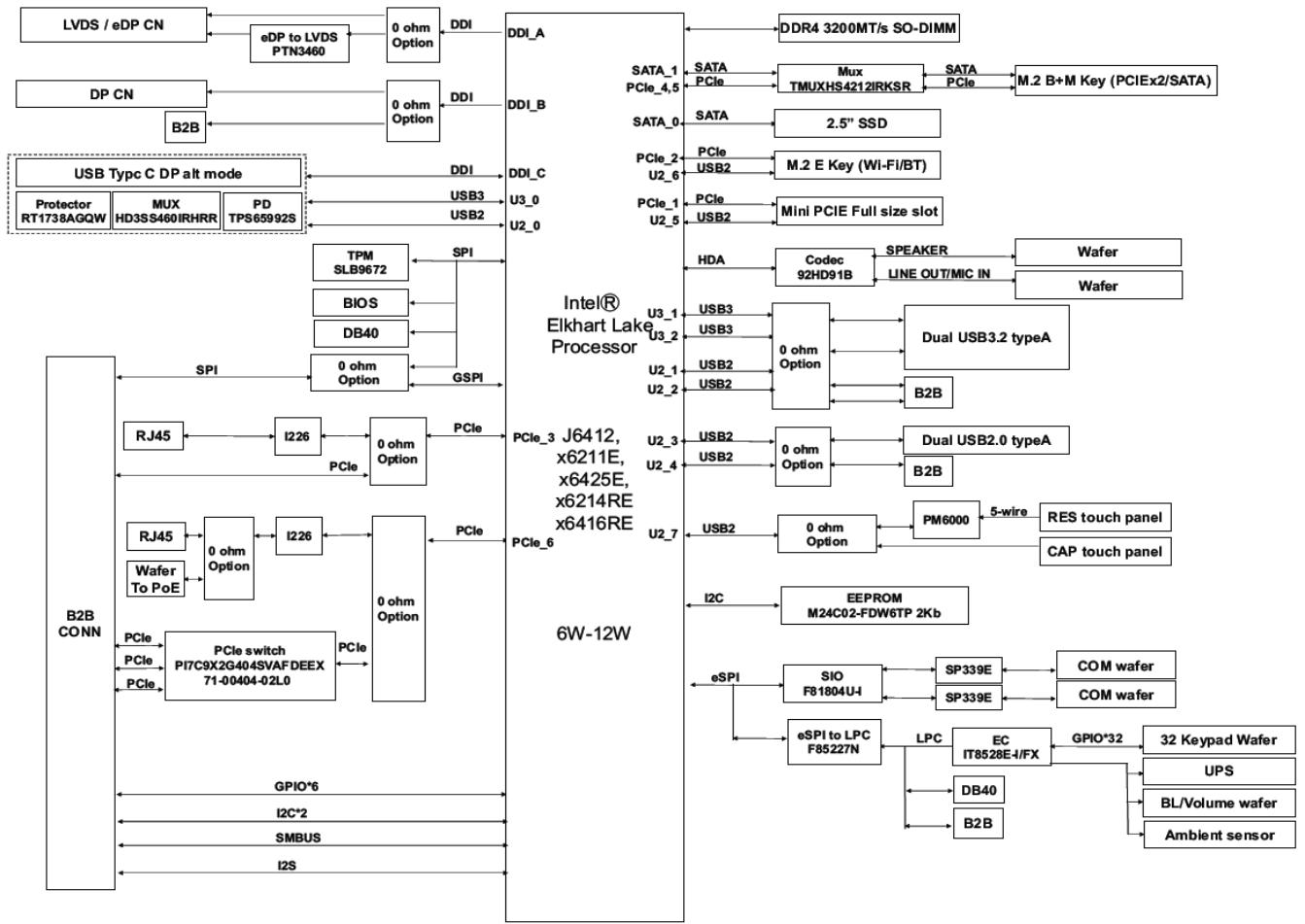
# 2.2 Functional Block Diagram

![This block diagram depicts the connectivity of an **Intel® Elkhart Lake Processor (6W-12W)** system. The processor acts as the central hub connecting various input/output interfaces, peripherals, and expansion slots.\n\n**Left Side (Inputs & Connectivity):**\n*   **Display Connections:**\n    *   **LVDS / eDP CN** connects to **eDP to LVDS PTN3460**, which connects to a **0 ohm Option**. This path connects via **DDI** to **DDI_A** on the processor.\n    *   **DP CN** connects to **B2B**, which connects to a **0 ohm Option**. This path connects via **DDI** to **DDI_B** on the processor.\n    *   **USB TypC DP alt mode** (containing **Protector RT1738AGQW**, **MUX HD3SS460IRHRR**, **PD TPS65992S**) connects via **DDI** to **DDI_C**, via **USB3** to **U3_0**, and via **USB2** to **U2_0**.\n*   **System Control:**\n    *   **TPM SLB9672** connects via **SPI** to **BIOS**, **DB40**, and a **0 ohm Option** (labeled **GSPI**).\n    *   **B2B CONN** connects via **SPI** to the TPM/BIOS block.\n    *   **B2B CONN** outputs **GPIO*6**, **I2C*2**, **SMBUS**, and **I2S**.\n*   **Network/PCIe:**\n    *   **B2B CONN** connects via **PCIe** to a **PCIe switch P17C9X2G404SVAFDEEX 71-00404-02L0**.\n    *   The PCIe switch connects via **PCIe** to a vertical **0 ohm Option** block, which connects to **PCIe_6** on the processor.\n    *   One **RJ45** connects to **I226**, which connects to a **0 ohm Option**, connecting via **PCIe** to **PCIe_3**.\n    *   Another **RJ45** and **Wafer To PoE** connect to a **0 ohm Option**, which connects to **I226**, then a **0 ohm Option**, then the vertical **0 ohm Option** block (connecting to **PCIe_6**).\n\n**Right Side (Outputs & Peripherals):**\n*   **Memory & Storage:**\n    *   **DDR4 3200MT/s SO-DIMM** connects to the processor.\n    *   **SATA_1 PCIe_4_5** connects to **Mux TMUXHS4212IRKSR**, which connects via **SATA PCIe** to **M.2 B+M Key (PCIEx2/SATA)**.\n    *   **SATA_0** connects to **2.5' SSD**.\n    *   **PCIe_2 U2_6** connects to **M.2 E Key (Wi-Fi/BT)**.\n    *   **PCIe_1 U2_5** connects to **Mini PCIE Full size slot**.\n*   **Audio:**\n    *   **HDA** connects to **Codec 92HD91B**.\n    *   The Codec connects to **SPEAKER** (outputting to **Wafer**) and **LINE OUT/MIC IN** (outputting to **Wafer**).\n*   **USB:**\n    *   **U3_1 U3_2** connect via **USB3** to a **0 ohm Option**, connecting to **Dual USB3.2 typeA**.\n    *   **U2_1 U2_2** connect via **USB2** to **B2B**.\n    *   **U2_3 U2_4** connect via **USB2** to a **0 ohm Option**, connecting to **Dual USB2.0 typeA**, which connects to **B2B**.\n    *   **U2_7** connects via **USB2** to a **0 ohm Option**, connecting to **PM6000**, which connects via **5-wire** to **RES touch panel** and **CAP touch panel**.\n*   **Super I/O & Embedded Controller:**\n    *   **I2C** connects to **EEPROM M24C02-FDW6TP 2Kb**.\n    *   **eSPI** connects to **SIO F81804U**, which connects via **SP339E** (x2) to **COM wafer** (x2).\n    *   **eSPI** connects to **eSPI to LPC F85227N**, which connects via **LPC** to **EC IT8528E-I/FX**.\n    *   The EC connects via **GPIO*32** to **32 Keypad Wafer**, **UPS**, **BL/Volume wafer**, and **Ambient sensor**.\n    *   **eSPI to LPC** also connects to **DB40** and **B2B**.](.sp2-ehl-50m-p1400-1010-11/799b4a871f6950b6b1211da4c173e558c3758e5cddb9d43d54a38b8a98d8fd57.jpg)

Figure 1: Functional block diagram

This page intentionally left blank.

# 3 Mechanical Layout

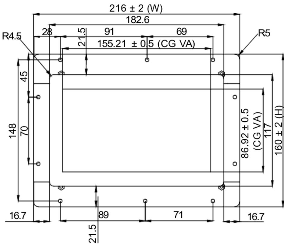
# 3.1 SP2-7WP Dimensions

![The image displays a simple icon of a white document or piece of paper with a folded top-right corner. Faint grey horizontal lines run across the page, simulating text. A large, red checkmark is prominently displayed over the document.](.sp2-ehl-50m-p1400-1010-11/150f8bbe3a072ce65b62906b58c27d7be8e1fc6ebb332426d261bfd343d01972.jpg)
NOTE:

All dimensions are in millimeters, unless noted.

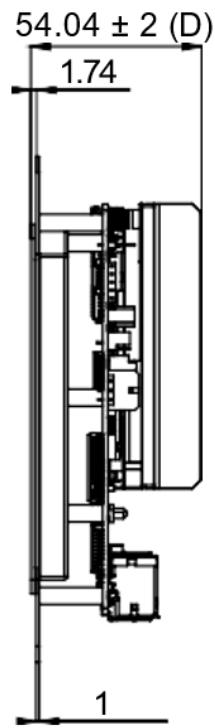
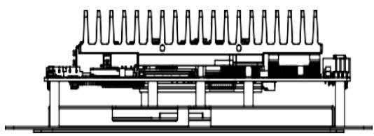
# 3.1.1 SP2-7WP Dimensions
![Technical line drawing of a mechanical assembly with multiple cylindrical components and a central housing (no text or symbols)](.sp2-ehl-50m-p1400-1010-11/de1b19711fe8a4ef09ced40a482aff22ce3ff2bad11131feb375be979b96a719.jpg)

![216 ± 2 (W)\n182.6\nR4.5\n28\n5\n91\n69\n21.5\n155.21 ± 0.5 (CG VA)\n45\n70\n148\n16.7\n89\n71\n21.5\nR5\n86.92 ± 0.5\n(CG VA)\n117\n160 ± 2 (H)\n16.7](.sp2-ehl-50m-p1400-1010-11/89d971dbbe4e6a28d7a1b52cd68c2b2280701047eecae873b7619c2c93f073cd.jpg)

![54.04 ± 2 (D)\n1.74\n1](.sp2-ehl-50m-p1400-1010-11/45fcb8f08436c0873bf10909c0aff548bb9c394ada253a68861b66a1c803a777.jpg)

Figure 2: SP2-7WP dimensions

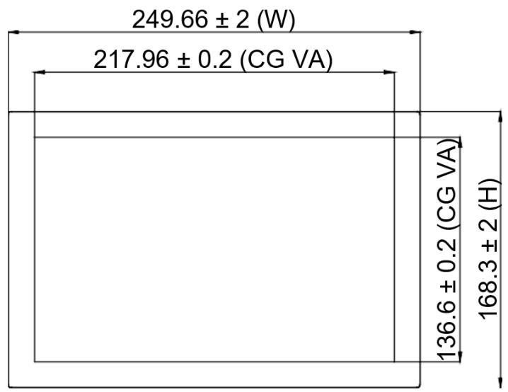
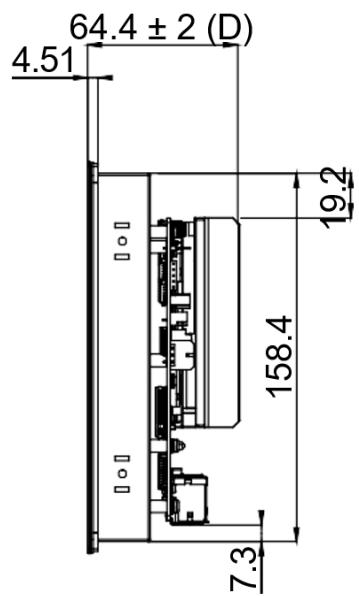
# 3.1.2 SP2-10WP Dimensions
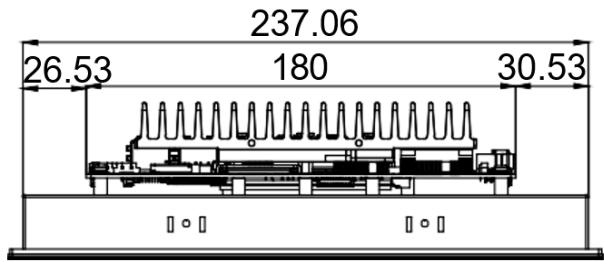
![237.06\n26.53 180 30.53](.sp2-ehl-50m-p1400-1010-11/6cca7d5da2f508f82df694c047e2fc5c5760d5192a937e85e32f338463373ca7.jpg)

![| Dimension | Value |\n| :--- | :--- |\n| Power (W) | 249.66 ± 2 |\n| CG VA (cm) | 217.96 ± 0.2 |\n| Height (H) | 168.3 ± 2 |\n| Width (cm) | 136.6 ± 0.2 |](.sp2-ehl-50m-p1400-1010-11/9f1ece8fc9a26a843c7335a534ef91189c7d0e720f14af5ca7b39e3c2b69bf95.jpg)

![64.4 ± 2 (D)\n4.51\n19.2\n158.4\n7.3](.sp2-ehl-50m-p1400-1010-11/a97f5a402df227cc74f66daadc88b875c0a1e7573024724d6fb9fda063a38ede.jpg)

Figure 3: SP2-10WP dimensions

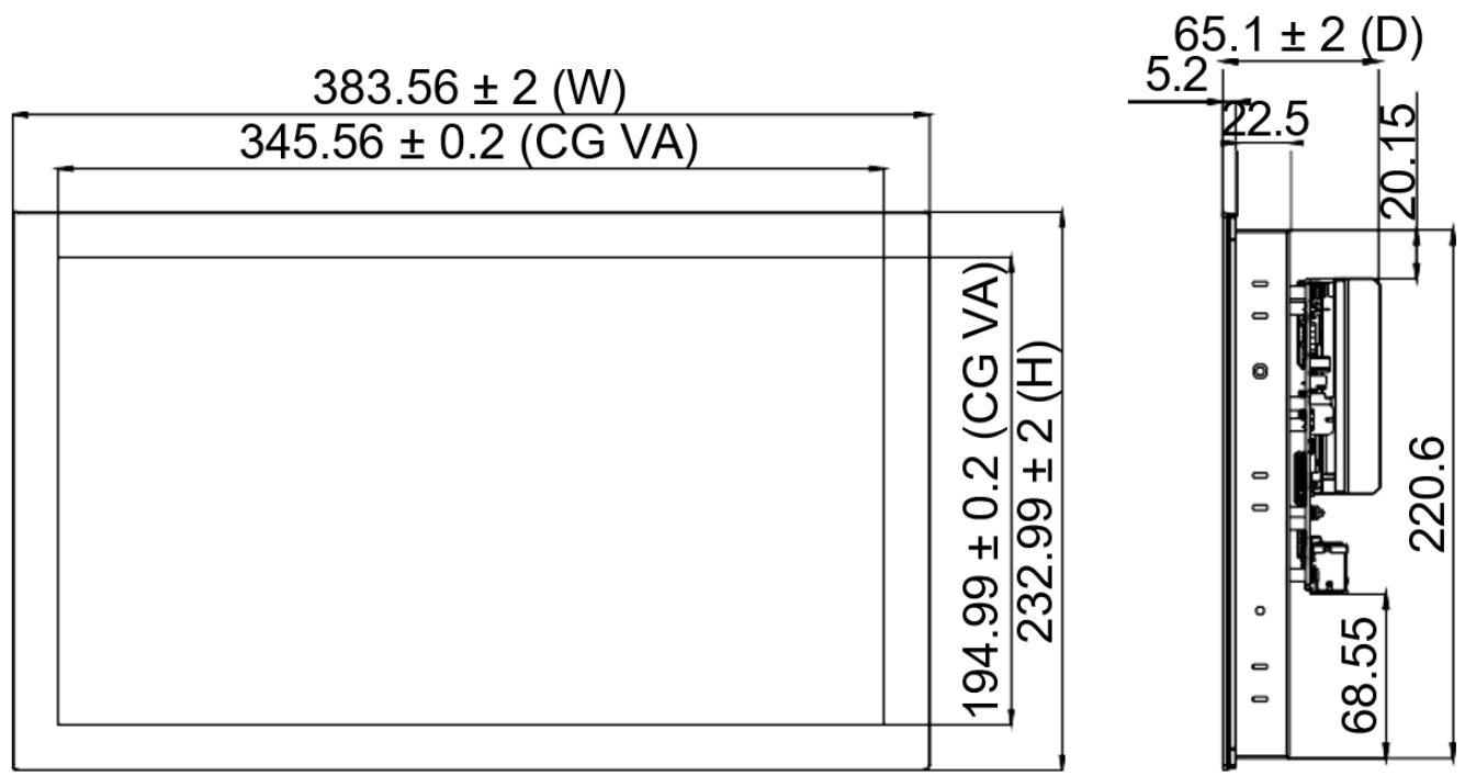
# 3.1.3 SP2-15WP Dimensions
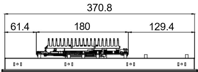
![| Dimension | Value |\n| --------- | ----- |\n| Total Length | 370.8 |\n| Segment Length | 61.4 |\n| Segment Height | 180 |\n| Segment Width | 129.4 |](.sp2-ehl-50m-p1400-1010-11/43f9fec7257f6d6ec6b55b0ceae85d205124da1d748d9578126dc7f0a217a4d1.jpg)

![| Dimension | Value     |\n| --------- | --------- |\n| Width     | 383.56 ± 2 (W) |\n| Height    | 345.56 ± 0.2 (CG VA) |\n| Height    | 194.99 ± 0.2 (CG VA) |\n| Height    | 232.99 ± 2 (H) |\n| Top Diameter | 65.1 ± 2 (D) |\n| Bottom Diameter | 68.55 |\n| Top Diameter (D) | 5.2 |\n| Bottom Diameter (D) | 22.5 |\n| Top Diameter (H) | 20.15 |\n| Bottom Diameter (H) | 220.6 |](.sp2-ehl-50m-p1400-1010-11/450cc903c69b5b8f3527b945f31699e2c82e76ef527b29cff8a4aa7439ea0325.jpg)

Figure 4: SP2-15WP dimensions

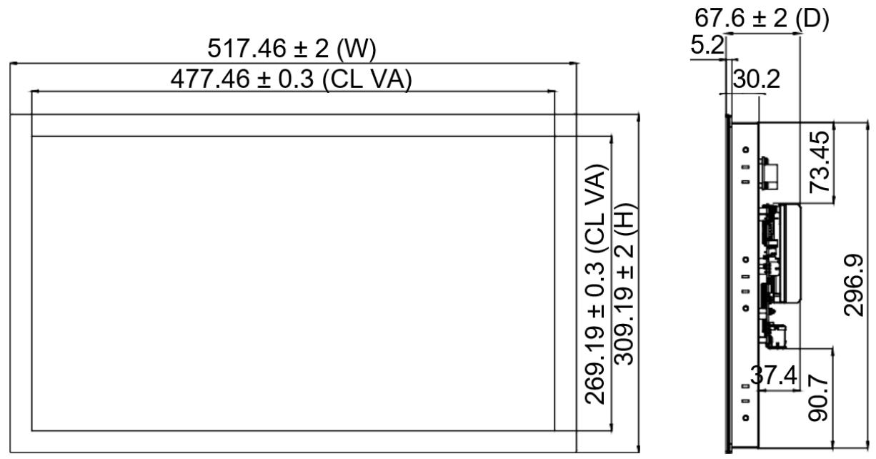
# 3.1.4 SP2-21WP Dimensions
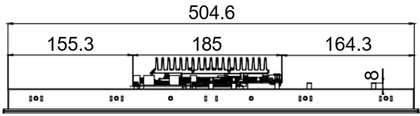
![| Dimension | Value |\n| --------- | ----- |\n| Total Length | 504.6 |\n| Top Height | 155.3 |\n| Bottom Height | 185 |\n| Bottom Width | ∞ |](.sp2-ehl-50m-p1400-1010-11/5982cc91cf73d9ebb575a9bbe31a2289fd4183c5a52491d99619737a2f10ed6a.jpg)

![| Dimension | Value       |\n| --------- | ----------- |\n| Width     | 517.46 ± 2 (W) |\n| Height    | 477.46 ± 0.3 (CL VA) |\n| Width     | 269.19 ± 0.3 (CL VA) |\n| Height    | 309.19 ± 2 (H) |\n| Width     | 67.6 ± 2 (D) |\n| Height    | 5.2         |\n| Width     | 30.2        |\n| Height    | 73.45       |\n| Width     | 296.9       |\n| Height    | 37.4        |\n| Width     | 90.7        |\n| Height    | 90.7        |](.sp2-ehl-50m-p1400-1010-11/7c107af60f6ad35583d479066aa00efafc4b6ecbb32cc368360cf4635c8aaeb0.jpg)

Figure 5: SP2-21WP dimensions

# 3.2 Thermal Options

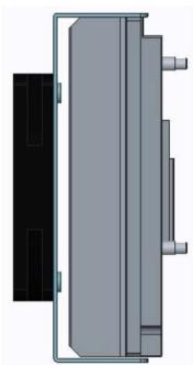
# 3.2.1 Active Cooling Heatsink
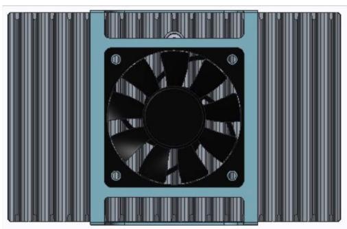
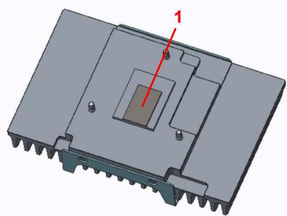
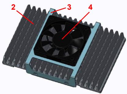
![Illustration of a black CPU fan with visible blades and mounting holes, mounted on a grid-patterned side panel (no text or symbols)](.sp2-ehl-50m-p1400-1010-11/e6f9562589b249df497c09210d08a9ddab1efbe91a2b3b6efa630c71e9286f1b.jpg)

![Pure technical diagram of a mechanical component without any text, numbers, or symbols](.sp2-ehl-50m-p1400-1010-11/ad8a6ddc29cc8faeda7d88add4c63e398facb39065de2f60c246df8ccc1a06bd.jpg)

![3D mechanical component diagram showing a layered structure with a highlighted section and red annotation line (no text or symbols)](.sp2-ehl-50m-p1400-1010-11/f3fe8a2cc0ce4075d25c71e64776dceab2aae0e78c4a03a03f696cb5ba7d9336.jpg)

![2\n3\n4](.sp2-ehl-50m-p1400-1010-11/28c5d87bba069a6e167fc9694dc0138986e9e6a10034ffd0b0c10bb084d0d6b9.jpg)

Figure 6: Active Cooling Heatsink

Table 1: Heatsink components

<table><tr><td>No.</td><td>Description</td><td>Part Number</td><td>Material</td><td>Dimensions</td><td>Remarks</td></tr><tr><td>1</td><td>TIM</td><td>N/A</td><td>PCM4988</td><td>25x15x0.2mm</td><td></td></tr><tr><td>2</td><td>Heat Sink</td><td>32-20614-4000-A0</td><td>AL6063</td><td>143x90x27.6mm</td><td></td></tr><tr><td>3</td><td>Fan Bracket</td><td>34-35121-0000-A0</td><td>SGCC</td><td>92.4x72x25mm</td><td></td></tr><tr><td>4</td><td>Fan</td><td>32-00086-3000-A0</td><td>Plastic</td><td>60x10mm</td><td>Axial Fan</td></tr></table>

# 3.2.2

# Heatsink Dimensions

![The image displays a white document icon featuring horizontal black lines representing text. A large, bold red checkmark is superimposed over the right side of the page.](.sp2-ehl-50m-p1400-1010-11/5d4314cb2cd5c7dae5022f252f1051a45578f294e50f782f216c1930e0d4ad7f.jpg)
NOTE:

All dimensions are in millimeters, unless noted.

![A yellow triangular warning sign with a black border containing a black exclamation point.](.sp2-ehl-50m-p1400-1010-11/14327b5f6f2176aa785090f82af12d4d1ffa41ee87e7ef49d516a4e9dd5fba69.jpg)
CAUTION:

Due to radiant heat from the passive heatsink, make sure the heatsink is positioned at least 10cm from the nearest wall.

![(143,07)\n28,15±0.15\n(27,6)\n90\n48,75±0.15\n28,75\n43,39\n56,29±0.15\nφ9\nφ4](.sp2-ehl-50m-p1400-1010-11/0703ae388fff97480825c3a91a2c99868a9ed3a5558c23fde362b2a27e9d8f7d.jpg)

Figure 7: Heatsink dimensions

# 3.2.3 Cable Routing Considerations for Heatsinks

Cable routing should avoid high temperature areas as shown below.

![Top-down schematic of a computer motherboard with red X-shaped annotations and circuit patterns (no readable text or symbols)](.sp2-ehl-50m-p1400-1010-11/4d86d5c2ad6c1343530ce6bfc89667f7c958fead60115e54f9df9ca65fde2986.jpg)

Figure 8: Cable routing considerations for heatsinks

![The image displays a white document icon with a folded top-right corner. Faint grey horizontal lines are visible on the paper, suggesting text. A large, bold red checkmark is superimposed over the center of the document.](.sp2-ehl-50m-p1400-1010-11/7d6b220ed7b4d3bec2e350b23f15d613d75f218883359d90b5ca525be108326a.jpg)
NOTE:

Heat sink design optimized for open-frame installations, such as a kiosk.

For panel PCs, a different design may be required. Consult your ADLINK sales representative for guidance.

# 4 Getting Started

Follow the instructions in this chapter to add or change memory; Wi-Fi modules, mounting brackets, and mounting clips.

# 4.1 Adding or Changing Memory

Follow these steps to add or change memory modules.

1. Remove the 3 screws that attach the heatsink to the mainboard, and then remove the heatsink.

![Technical diagram of an electronic device rear panel with connectors and ports, no visible text or symbols](.sp2-ehl-50m-p1400-1010-11/165d8299f9329f03d1f8cbe3ee867efbb4844dc177a7dc581c44a13b4d940f39.jpg)

2. Install or swap the memory module in the SODIMM socket as necessary.

![Top-down schematic of an electronic circuit board with UDE connectors and a highlighted component (no text or symbols)](.sp2-ehl-50m-p1400-1010-11/e731caba8048eb6662f94c083f23c17de8fb80436a1fdedebed73a4ee13a6c9b.jpg)

3. Reattach the heat sink to the mainboard with the previously removed screws.

# 4.2 Installing a Wi-Fi-Module

Follow these steps to add or change a Wi-Fi modules.

![A white document icon featuring a folded top corner and faint grey horizontal lines is overlaid with a large, bold red checkmark.](.sp2-ehl-50m-p1400-1010-11/bc471cc74c901b477270f0867897b2a39bc207c14fff5f785bd119248ff410f4.jpg)
NOTE:

In the default configuration, only one PCI slot is available. Choose either a Wi-Fi module or a 4G/5G module.

1. Remove the 3 screws that attach the heatsink to the mainboard, and then remove the heatsink.

![Technical diagram of an electronic device rear panel with connectors and ports (no text or labels)](.sp2-ehl-50m-p1400-1010-11/5e7e309f3f600c93b7f528e8f199cfbdc1a444d1189287707a03a8267763e9fe.jpg)

2. Install the Wi-Fi module.

![Top-down schematic of a computer motherboard layout with CPU socket, RAM slots, and UDE connectors (no text or labels)](.sp2-ehl-50m-p1400-1010-11/cc3dd041f735c3598572b85cf455ffb85bee23f6fb39da78aa6c60fedab13e06.jpg)

3. Reattach the heat sink to the mainboard with the previously removed screws.

![The image displays a white document icon with a folded top-right corner and faint grey horizontal lines, overlaid with a large red checkmark.](.sp2-ehl-50m-p1400-1010-11/9d42a6778e63ba12d678a065a1cabf4093668d6187612206b8ba4f4df5daa9e8.jpg)
NOTE:

Wi-Fi antennas must be installed on the SP2-EHL Series housing in order for Wi-Fi to function properly.

# 4.3 Mounting

This section includes details for panel and VESA mounting options.

![The image shows a standard warning symbol consisting of a red equilateral triangle pointing upward. Inside the red triangle is a large white exclamation point. The background is white, and the entire graphic is framed by a thin black border.](.sp2-ehl-50m-p1400-1010-11/5855d7e755f3b821b08becc3b9ee0c9b8ac1702ba2a003a3373ef98342ed4964.jpg)
WARNING:

Risk of physical injuries and / or property damage:

When mounting the device, use the screws to mount the VESA bracket to the rear of the device. Tighten all four screws firmly to support the weight of the device. Make sure that the suspension system is capable of carrying the device.

![A yellow triangular warning sign with a thick black border, containing a large black exclamation point in the center.](.sp2-ehl-50m-p1400-1010-11/ae9f5f82598d3157370c4cd9211c9b854de36201043cdc9dc5e94fce38f967b9.jpg)
CAUTION:

Risk of burns to the user caused by hot surfaces:

Turn off power and allow the device to cool down prior to per- forming any mounting or demounting operations. Do not touch the enclosure for over 10 seconds when the device is in operation or is still hot from previous use.

![A white document icon featuring horizontal black lines is overlaid with a large red checkmark.](.sp2-ehl-50m-p1400-1010-11/72b1bcf1fd71f401ecf3fd98d44cf9f87d2694bef79552078b16f2acafbaadff.jpg)
NOTE:

All dimensions are in millimeters, unless noted.

# 4.3.1 Panel Mounting

The SP2-EHL Series can be panel mounted with 14 mounting clips (optional items sold separately). Make sure there is adequate space behind the panel for ventilation, and that the panel material and thickness can support the weight of the device.

Step 1: Cut the panel opening using the appropriate cutout dimensions.

![181 ± 0.5\nDVU PVU\n131 ± 0.5](.sp2-ehl-50m-p1400-1010-11/2b007a30fc227848aa8713809d28993fe186aa56dfb9b75abc82946025f1b031.jpg)

Figure 9: SP2-7WP cutout dimensions

![238.06 ± 0.5\nDVU PVU\n159.4 ± 0.5](.sp2-ehl-50m-p1400-1010-11/f904f76bebb151dd0207466857d5ff6ec8b5c6db7037e4d72c844b8d5fdd5c95.jpg)

Figure 10: SP2-10WP cutout dimensions

Step 2: Attach I/O cables to the device before installing into the panel if rear access will be limited after installation.

Step 3: Place the device into the panel cutout.

![Diagram showing two rectangular panels with a red arrow indicating direction, no text or symbols present](.sp2-ehl-50m-p1400-1010-11/f9441ec95aced5ad422ce83db93707f503f5b955b4b9dcff248e2e99b62bac9a.jpg)

Step 4: Insert the mounting clips into the slots on the sides of the device as shown. Hand-tighten the mounting clips with a Phillips- head screwdriver to secure it to the panel. Do not overtighten the clips to avoid damaging the device enclosure.

![1.2\n1.2\n1.2\nPOWER\nBAN\nBLUT\n+\n-\nDIN-10\nVOUT\n10A\nCLIP](.sp2-ehl-50m-p1400-1010-11/c5b91c4cdb37425aeaafd5d4eae8b2fd6ca9c98418de4175933ee60b69545053.jpg)

![The image displays a technical engineering drawing of a mechanical bracket assembly with a screw, presented through multiple orthographic and isometric views.\n\n**Top Section:**\n*   **Left:** A front view showing a horizontal dimension of **14.2** with tolerances **+0.3** and **-0.1**, and a vertical dimension of **5.7**.\n*   **Center:** A top view showing the bracket and screw head.\n*   **Right:** An isometric 3D view showing the screw inserted into a U-shaped bracket.\n\n**Bottom Section:**\n*   **Left:** A side view showing a total height of **16.7 ± 0.3** and a top width of **12**.\n*   **Center:** A detailed side view with the text label **CROSS_P_NI_M4** pointing to the screw head and **TAP M4** pointing to the threaded hole. It features a total height dimension of **26.5** (tolerances **+0.1** and **-0.5**), a vertical spacing of **12**, and a width of **1.2**.\n*   **Right:** A side view showing vertical dimensions of **5** and **3**, and a horizontal dimension of **1.3**.](.sp2-ehl-50m-p1400-1010-11/b72de3e41bfcf2b02da6b7fbedb82d1e9f01b9d9b5f1eda363b3f8cae7d0b7a4.jpg)
Figure 11: Mounting clip dimensions

![This image shows an icon of a white document with horizontal black lines. The top right corner of the document is folded down. A large, thick red checkmark is superimposed over the center of the document.](.sp2-ehl-50m-p1400-1010-11/cd58a42f546f518d93d27fc2c0e6cb8a6368ac13f1a1fb7699dd82722b4b8718.jpg)
NOTE:

Optional mounting clips sold separately. Contact your ADLINK reseller for details.

# 4.3.2 VESA Mounting

The SP2-EHL Series can be VESA mounted with a rear cover and VESA bracket. (Optional items sold separately.)

![The image displays a white document icon with horizontal black lines, overlaid with a large red checkmark.](.sp2-ehl-50m-p1400-1010-11/5859d02e3d1a6fc2422861e895e6ed8a03e635e0e22a941194ecac48f57e0aca.jpg)
NOTE:

1. All I/O ports must face down.
2. Optional VESA bracket and M3 screws sold separately. Contact your ADLINK reseller for details.
3. Mounting bracket provides 100 mm x 100 mm VESA mounting and requires 4x M4 screws.

Step 1: Attach the rear cover to the panel PC with the screws supplied in the kit.

![Rear Cover](.sp2-ehl-50m-p1400-1010-11/4364ee1825e3f967a719715e061d644dfc2578864a143832444f164c9330845f.jpg)

Step 2: Attach the VESA bracket to the rear cover with 4x M3 screws.

![VESA Bracket](.sp2-ehl-50m-p1400-1010-11/9dc88560f615df94f8634e88c109869bef37a1b846fd8065fccad5debdd61687.jpg)

This page intentionally left blank.

# 5 System Layout

# 5.1 External I/O Connectors

The SP2-EHL Series provides the following external I/O connectors.

![A\nB\nC\nD\nE](.sp2-ehl-50m-p1400-1010-11/5c5243dc5618454ecacac68462b9f2dc037e70ba0cc0af42c10001a32c917cb2.jpg)

Figure 12: External I/O connectors

Table 2: External I/O legend

<table><tr><td>A</td><td>1x USB 3.1 Gen 1, Type-C</td></tr><tr><td>B</td><td>2x USB 3.2 Gen1 (5Gbps) Type-A</td></tr><tr><td>C</td><td>2x USB 2.0 Type-A</td></tr><tr><td>D</td><td>1x DisplayPort</td></tr><tr><td>E</td><td>2x RJ45 GbE LAN</td></tr></table>

# 5.2 Internal I/O Connectors

![The image displays a standard warning symbol featuring a maroon triangle pointing upward with a white exclamation mark centered inside it.](.sp2-ehl-50m-p1400-1010-11/971acd52b6f8051d02657e48e74f2bff1ee07431dcea42cbbd0141d8dd3e8f40.jpg)
WARNING:

Installation of add-on devices must be carried out by ADLINK service personnel only. Users must not disassemble the device themselves.

L'installation de périphériques complémentaires doit être effec- tuée uniquement par le personnel de service ADLINK. Les util- isateurs ne doivent pas démonter l'appareil eux-mêmes.

# 5.2.1 Mainboard Connector Locations

![E F G H I J K\nD C B A L M N O P Q R S T U](.sp2-ehl-50m-p1400-1010-11/2acf816344cccd754334490c7bbd94c28755561b03909213c9624eef403ee2f8.jpg)

Figure 13: Mainboard connectors (Top)

![AA\nAB\nAC\nZ\nY\nX\nW\nV\nAD\nAE](.sp2-ehl-50m-p1400-1010-11/dfa1e891f6261a8a040572d25e8831ef3f0fbfcca431c935c11ff938dce9bcca.jpg)

Figure 14: Mainboard connectors (Bottom)

Table 3: Mainboard connector legend

<table><tr><td>A</td><td>Power connector</td><td>Q</td><td>Volume &amp; Backlight Control Connector</td></tr><tr><td>B</td><td>SATA Power Connector</td><td>R</td><td>Key Connector</td></tr><tr><td>C</td><td>SATA Data Connector</td><td>S</td><td>Fan Connector</td></tr><tr><td>D</td><td>Resistive Touch Connector</td><td>T</td><td>Clear CMOS Jumper</td></tr><tr><td>E</td><td>Capacitive Touch Connector</td><td>U</td><td>PoE Module (Optional)</td></tr><tr><td>F</td><td>Mini PCIe connector</td><td>V</td><td>COM2 Connector</td></tr><tr><td>G</td><td>M.2 2230, E Key for Wi-Fi/Bluetooth Modules</td><td>W</td><td>COM1 Connector</td></tr><tr><td>H</td><td>Function Module</td><td>X</td><td>LED Connector</td></tr><tr><td>I</td><td>LVDS/eDP Connector</td><td>Y</td><td> $I^{2}C$  Connector-1</td></tr><tr><td>J</td><td>SO-DIMM Slot</td><td>Z</td><td> $I^{2}C$  Connector-2</td></tr><tr><td>K</td><td>Power/Reset/LED Button</td><td>AA</td><td>RTC Battery Connector</td></tr><tr><td>L</td><td>Buzzer Connector</td><td>AB</td><td>DB40 Connector</td></tr><tr><td>M</td><td>Mic-in/Line-out</td><td>AC</td><td>GPIO Connector</td></tr><tr><td>N</td><td>Speaker</td><td>AD</td><td>UPS Connector</td></tr><tr><td>O</td><td>USB 2.0 Connector</td><td>AE</td><td>M.2 M Key Connector</td></tr><tr><td>P</td><td>USB 2.0 Connector</td><td></td><td></td></tr></table>

This page intentionally left blank.

# 6 Connector Pinouts and Jumper Settings

# 6.1 Power Connector

The 6-pin power connector connects an AC/DC power supply adapter, DC-to-DC power, module and battery. Supports AT and ATX power modes, with AT mode controlled by the BIOS.

<table><tr><td>Pin</td><td>Signal</td></tr><tr><td>1</td><td>GND</td></tr><tr><td>2</td><td>GND</td></tr><tr><td>3</td><td>GND</td></tr><tr><td>4</td><td>PWR_CONN_IN</td></tr><tr><td>5</td><td>PWR_CONN_IN</td></tr><tr><td></td><td>PWR_CONN_IN</td></tr></table>

![Pure electrical circuit lines without any symbols](.sp2-ehl-50m-p1400-1010-11/28e6f05a3259bbe687650b75588aa9a20007d43608b9c875332c9443453915bc.jpg)

# 6.2 SATA Power Connector

The SATA power connector provides a power connection for an internal $_ { 2 . 5 " }$ HDD.

<table><tr><td>Pin</td><td>Signal</td></tr><tr><td>1</td><td>NC</td></tr><tr><td>2</td><td>GND</td></tr><tr><td>3</td><td>P+5V_S0</td></tr><tr><td>4</td><td>GND</td></tr><tr><td>5</td><td>P+3V3_S0</td></tr></table>

![Pure electrical circuit lines without any symbols](.sp2-ehl-50m-p1400-1010-11/84ae7894b875275ffbb646e2c79676aeff59bb5e48f3670b8495a59cf43364a7.jpg)

# 6.3 SATA Data Connector

<table><tr><td>Pin</td><td>Signal</td></tr><tr><td>1</td><td>GND</td></tr><tr><td>2</td><td>SATA_TX1_P</td></tr><tr><td>3</td><td>SATA_TX1_N</td></tr><tr><td>4</td><td>GND</td></tr><tr><td>5</td><td>SATA_RX1_N</td></tr><tr><td>6</td><td>SATA_RX1_P</td></tr><tr><td>7</td><td>GND</td></tr></table>

![Pure architectural floor plan lines without any text, numbers, or symbols](.sp2-ehl-50m-p1400-1010-11/1d785be7323cda93ded039f73773e5796c7c0be3cbd3f82fe7ebfc70a599e6fb.jpg)

# 6.4 Resistive Touch Connector

The internal USB 2.0 connector supports a resistive digitizer.

<table><tr><td>Pin</td><td>Signal</td></tr><tr><td>1</td><td>X-</td></tr><tr><td>2</td><td>Y-</td></tr><tr><td>3</td><td>SENSE</td></tr><tr><td>4</td><td>X+</td></tr><tr><td>5</td><td>Y+</td></tr></table>

![Pure electrical circuit lines without any symbols](.sp2-ehl-50m-p1400-1010-11/fe8dd68d56ec81d923a9b399410bd269efafd118038c61a7e993e9cc29e96bf1.jpg)

# 6.5 Capacitative Touch Connector

<table><tr><td>Pin</td><td>Signal</td></tr><tr><td>1</td><td>GND</td></tr><tr><td>2</td><td>TSC_D+</td></tr><tr><td>3</td><td>TSC_D-</td></tr><tr><td>4</td><td>P5V_U2TOU</td></tr></table>

![Pure electrical circuit lines without any symbols](.sp2-ehl-50m-p1400-1010-11/6a7bd5f7bd9968115ea3aa6c15392076fc7a4d3dbc8c8c80545ed9b6146d47ee.jpg)

# 6.6 Mini PCIe Connector

The mini PCIe connector supports standard PCIe signals such as PCIe Gen4 and USB2.0.

<table><tr><td>Pin</td><td>Signal</td><td>Pin</td><td>Signal</td></tr><tr><td>1</td><td>PCIE_WAKE-L</td><td>2</td><td>P_+3V3_S0_mPCIe</td></tr><tr><td>3</td><td>TP point</td><td>4</td><td>GND</td></tr><tr><td>5</td><td>TP point</td><td>6</td><td>P_+1V5_S0_mPCIe</td></tr><tr><td>7</td><td>PCH_CLK_REQ3-L</td><td>8</td><td>X</td></tr><tr><td>9</td><td>GND</td><td>10</td><td>X</td></tr><tr><td>11</td><td>MPCIE_CLK3_N</td><td>12</td><td>X</td></tr><tr><td>13</td><td>MPCIE_CLK3_P</td><td>14</td><td>X</td></tr><tr><td>15</td><td>GND</td><td>16</td><td>X</td></tr><tr><td>17</td><td>X</td><td>18</td><td>GND</td></tr><tr><td>19</td><td>X</td><td>20</td><td>TP point</td></tr><tr><td>21</td><td>GND</td><td>22</td><td>PLTRST-L_MINIPCIE</td></tr><tr><td>23</td><td>MPCIE_RX6_N</td><td>24</td><td>P_+3V3_S0_mPCIe</td></tr><tr><td>25</td><td>MPCIE_RX6_P</td><td>26</td><td>GND</td></tr><tr><td>27</td><td>GND</td><td>28</td><td>P_+1V5_S0_mPCIe</td></tr><tr><td>29</td><td>GND</td><td>30</td><td>PCH_SMB_CLK_MINI</td></tr><tr><td>31</td><td>MPCIE_TX6_N_C</td><td>32</td><td>PCH_SMB_DAT_MINI</td></tr><tr><td>33</td><td>MPCIE_TX6_P_C</td><td>34</td><td>GND</td></tr><tr><td>35</td><td>GND</td><td>36</td><td>USB_MINIPCIE_N</td></tr><tr><td>37</td><td>GND</td><td>38</td><td>USB_MINIPCIE_P</td></tr><tr><td>39</td><td>P_+3V3_S0_mPCIe</td><td>40</td><td>GND</td></tr><tr><td>41</td><td>P_+3V3_S0_mPCIe</td><td>42</td><td>X</td></tr><tr><td>43</td><td>GND</td><td>44</td><td>TP point</td></tr><tr><td>45</td><td>X</td><td>46</td><td>X</td></tr><tr><td>47</td><td>X</td><td>48</td><td>P_+1V5_S0_mPCIe</td></tr><tr><td>49</td><td>X</td><td>50</td><td>GND</td></tr><tr><td>51</td><td>X</td><td>52</td><td>P_+3V3_S0_mPCIe</td></tr></table>

![Technical line drawing of an electronic component with slots and connectors (no text or symbols)](.sp2-ehl-50m-p1400-1010-11/35b7a5bcabac16adae02b7eedc293cac7426774371ef9ded0c47c929215f4a5c.jpg)

# 6.7 M.2 2230, E Key for Wi-Fi/Bluetooth Modules

Connects to power, reset button, and power LED via cable.

<table><tr><td>Pin</td><td>Signal</td><td>Pin</td><td>Signal</td></tr><tr><td>1</td><td>GND</td><td>2</td><td>P_+3V3_NGFF_E</td></tr><tr><td>3</td><td>M2E_USB_P</td><td>4</td><td>P_+3V3_NGFF_E</td></tr><tr><td>5</td><td>M2E_USB_N</td><td>6</td><td>NC</td></tr><tr><td>7</td><td>GND</td><td>8</td><td>NC</td></tr><tr><td>9</td><td>NC</td><td>10</td><td>NC</td></tr><tr><td>11</td><td>NC</td><td>12</td><td>NC</td></tr><tr><td>13</td><td>NC</td><td>14</td><td>NC</td></tr><tr><td>15</td><td>NC</td><td>16</td><td>NC</td></tr><tr><td>17</td><td>NC</td><td>18</td><td>GND</td></tr><tr><td>19</td><td>NC</td><td>20</td><td>NC</td></tr><tr><td>21</td><td>NC</td><td>22</td><td>NC</td></tr><tr><td>23</td><td>NC</td><td>32</td><td>NC</td></tr><tr><td>33</td><td>GND</td><td>34</td><td>NC</td></tr><tr><td>35</td><td>PCIE2_M2E_TX_P</td><td>36</td><td>NC</td></tr><tr><td>37</td><td>PCIE2_M2E_TX_N</td><td>38</td><td>NC</td></tr><tr><td>39</td><td>GND</td><td>40</td><td>NC</td></tr><tr><td>41</td><td>PCIE2_RX_P</td><td>42</td><td>NC</td></tr><tr><td>43</td><td>PCIE2_RX_N</td><td>44</td><td>NC</td></tr><tr><td>45</td><td>GND</td><td>46</td><td>NC</td></tr><tr><td>47</td><td>PCIECLK1_100M_P</td><td>48</td><td>NC</td></tr><tr><td>49</td><td>PCIECLK1_100M_N</td><td>50</td><td>NC</td></tr><tr><td>51</td><td>GND</td><td>52</td><td>M2E_PLTRST_BUF-L</td></tr><tr><td>53</td><td>PCH_CLK_REQ1-L</td><td>54</td><td>NC</td></tr><tr><td>55</td><td>M2_E_PEWAKE_N</td><td>56</td><td>W_DISABLE1</td></tr><tr><td>57</td><td>GND</td><td>58</td><td>PCH_SMB_DAT_A</td></tr><tr><td>59</td><td>NC</td><td>60</td><td>PCH_SMB_CLK_A</td></tr><tr><td>61</td><td>NC</td><td>62</td><td>GP_C02_SMB_ALERT-</td></tr><tr><td>63</td><td>GND</td><td>64</td><td>NC</td></tr><tr><td>65</td><td>NC</td><td>66</td><td>NC</td></tr><tr><td>67</td><td>NC</td><td>68</td><td>NC</td></tr><tr><td>69</td><td>GND</td><td>70</td><td>NC</td></tr><tr><td>71</td><td>NC</td><td>72</td><td>P_+3V3_NGFF_E</td></tr><tr><td>73</td><td>NC</td><td>74</td><td>P_+3V3_NGFF_E</td></tr><tr><td>75</td><td>GND</td><td></td><td></td></tr></table>

![Pure mechanical component diagram without any text, numbers, or symbols](.sp2-ehl-50m-p1400-1010-11/7126795730ed5d2c067205661c9f3dad22d5cfb7f05e84e88c9859e1d04534bb.jpg)

# 6.8 Function Module Board Connector

The function module allows customized expandability of the device. Contact your ADLINK representative for details.

<table><tr><td>Pin</td><td>Signal</td><td>Pin</td><td>Signal</td></tr><tr><td>1</td><td>P_+12V_A</td><td>2</td><td>P_+12V_A</td></tr><tr><td>3</td><td>P_+12V_A</td><td>4</td><td>P_+12V_A</td></tr><tr><td>5</td><td>GND</td><td>6</td><td>GND</td></tr><tr><td>7</td><td>GND</td><td>8</td><td>GND</td></tr><tr><td>9</td><td>P_+5V_A</td><td>10</td><td>P_+5V_A</td></tr><tr><td>11</td><td>P_+5V_A</td><td>12</td><td>P_+5V_A</td></tr><tr><td>13</td><td>GND</td><td>14</td><td>GND</td></tr><tr><td>15</td><td>GND</td><td>16</td><td>GND</td></tr><tr><td>17</td><td>P_+3V3_A</td><td>18</td><td>P_+3V3_A</td></tr><tr><td>19</td><td>P_+3V3_A</td><td>20</td><td>P_+3V3_A</td></tr><tr><td>21</td><td>GND</td><td>22</td><td>GND</td></tr><tr><td>23</td><td>GND</td><td>24</td><td>GND</td></tr><tr><td>25</td><td>PCH_SLP_S3-L</td><td>26</td><td>FM_I2C6_SDA_A</td></tr><tr><td>27</td><td>PCH_PCIE_FM_WAKE-L</td><td>28</td><td>FM_I2C6_SCL_A</td></tr><tr><td>29</td><td>GND</td><td>30</td><td>FM_PRESET-L</td></tr><tr><td>31</td><td>SOC_FM_PCIECLK2_P</td><td>32</td><td>PLTRST-L_FM</td></tr><tr><td>33</td><td>SOC_FM_PCIECLK2_N</td><td>34</td><td>GND</td></tr><tr><td>35</td><td>GND</td><td>36</td><td>GP_C02_SMB_ALERT-</td></tr><tr><td>37</td><td>SOC_FM_PCIE_RX3_P</td><td>38</td><td>PCH_SMB_DAT_A</td></tr><tr><td>39</td><td>SOC_FM_PCIE_RX3_N</td><td>40</td><td>PCH_SMB_CLK_A</td></tr><tr><td>41</td><td>GND</td><td>42</td><td>GND</td></tr><tr><td>43</td><td>SOC_FM_PCIE_TX3_P</td><td>44</td><td>FM_U3_TX1_P</td></tr><tr><td>45</td><td>SOC_FM_PCIE_TX3_N</td><td>46</td><td>FM_U3_TX1_N</td></tr><tr><td>47</td><td>GND</td><td>48</td><td>GND</td></tr><tr><td>49</td><td>SW_PCIE_CLK1_P</td><td>50</td><td>FM_U3_RX1_P</td></tr><tr><td>51</td><td>SW_PCIE_CLK1_N</td><td>52</td><td>FM_U3_RX1_N</td></tr><tr><td>53</td><td>GND</td><td>54</td><td>GND</td></tr><tr><td>55</td><td>FM_PCIE_RX1_P</td><td>56</td><td>FM_U2_P1_P</td></tr><tr><td>57</td><td>FM_PCIE_RX1_N</td><td>58</td><td>FM_U2_P1_N</td></tr><tr><td>59</td><td>GND</td><td>60</td><td>GND</td></tr><tr><td>61</td><td>FM_PCIE_TX1_P</td><td>62</td><td>FM_U3_TX2_P</td></tr><tr><td>63</td><td>FM_PCIE_TX1_N</td><td>64</td><td>FM_U3_TX2_N</td></tr><tr><td>65</td><td>GND</td><td>66</td><td>GND</td></tr><tr><td>67</td><td>SW_PCIE_CLK2_P</td><td>68</td><td>FM_U3_RX2_P</td></tr><tr><td>69</td><td>SW_PCIE_CLK2_N</td><td>70</td><td>FM_U3_RX2_N</td></tr><tr><td>71</td><td>GND</td><td>72</td><td>GND</td></tr><tr><td>73</td><td>FM_PCIE_RX2_P</td><td>74</td><td>FM_U2_P2_P</td></tr><tr><td>75</td><td>FM_PCIE_RX2_N</td><td>76</td><td>FM_U2_P2_N</td></tr><tr><td>77</td><td>GND</td><td>78</td><td>GND</td></tr><tr><td>79</td><td>FM_PCIE_TX2_P</td><td>80</td><td>FM_U2_P3_P</td></tr><tr><td>81</td><td>FM_PCIE_TX2_N</td><td>82</td><td>FM_U2_P3_N</td></tr><tr><td>83</td><td>GND</td><td>84</td><td>GND</td></tr><tr><td>85</td><td>SW_PCIE_CLK3_P</td><td>86</td><td>FM_U2_P4_P</td></tr><tr><td>87</td><td>SW_PCIE_CLK3_N</td><td>88</td><td>FM_U2_P4_N</td></tr><tr><td>89</td><td>GND</td><td>90</td><td>GND</td></tr></table>

![Pure technical line drawing of a mechanical component without any text, numbers, or symbols](.sp2-ehl-50m-p1400-1010-11/bb78b37e0daa13e71c96cdf0b45be0d965e0f9b8a1c2910cef61ea7f1be5d538.jpg)

<table><tr><td>91</td><td>FM_PCIE_RX3_P</td><td>92</td><td>LPC_AD0_R</td></tr><tr><td>93</td><td>FM_PCIE_RX3_N</td><td>94</td><td>LPC_AD1_R</td></tr><tr><td>95</td><td>GND</td><td>96</td><td>LPC_AD2_R</td></tr><tr><td>97</td><td>FM_PCIE_TX3_P</td><td>98</td><td>LPC_AD3_R</td></tr><tr><td>99</td><td>FM_PCIE_TX3_N</td><td>100</td><td>LPC_FRAME-L_R</td></tr><tr><td>101</td><td>GND</td><td>102</td><td>LPC_CLK0</td></tr><tr><td>103</td><td>PCH_CLK_REQ2-L</td><td>104</td><td>LPC_SERIRQ_R</td></tr><tr><td>105</td><td>FM_CLK_REQ123-L</td><td>106</td><td>LPC_DRQn_FM</td></tr><tr><td>107</td><td>GND</td><td>108</td><td>GND</td></tr><tr><td>109</td><td>FM_DDI1_TX0_P</td><td>110</td><td>I2S1_TXD</td></tr><tr><td>111</td><td>FM_DDI1_TX0_N</td><td>112</td><td>I2S1_RXD</td></tr><tr><td>113</td><td>GND</td><td>114</td><td>I2S1_SFRM</td></tr><tr><td>115</td><td>FM_DDI1_TX1_P</td><td>116</td><td>I2S1_SCLK</td></tr><tr><td>117</td><td>FM_DDI1_TX1_N</td><td>118</td><td>I2S_MCLK1</td></tr><tr><td>119</td><td>GND</td><td>120</td><td>GND</td></tr><tr><td>121</td><td>FM_DDI1_TX2_P</td><td>122</td><td>USB_OC2-L_R</td></tr><tr><td>123</td><td>FM_DDI1_TX2_N</td><td>124</td><td>USB_OC3-L_R</td></tr><tr><td>125</td><td>GND</td><td>126</td><td>GND</td></tr><tr><td>127</td><td>FM_DDI1_TX3_P</td><td>128</td><td>FM_GPIO0</td></tr><tr><td>129</td><td>FM_DDI1_TX3_N</td><td>130</td><td>FM_GPIO1</td></tr><tr><td>131</td><td>GND</td><td>132</td><td>FM_GPIO2</td></tr><tr><td>133</td><td>FM_DDI1_I2CCLK_AUX_P_CN</td><td>134</td><td>FM_GPIO3</td></tr><tr><td>135</td><td>FM_DDI1_I2CDAT_AUX_N_CN</td><td>136</td><td>FM_GPIO4</td></tr><tr><td>137</td><td>GND</td><td>138</td><td>FM_GPIO5</td></tr><tr><td>139</td><td>FM_DDI1_DDC_AUX_SEL_CN</td><td>140</td><td>FM_SPI_MISO</td></tr><tr><td>141</td><td>FM_DDI1_HPD</td><td>142</td><td>FM_SPI_MOSI</td></tr><tr><td>143</td><td>GND</td><td>144</td><td>FM_SPI_CS#</td></tr><tr><td>145</td><td>FM_I2C7_SDA_A</td><td>146</td><td>FM_SPI_CLK</td></tr><tr><td>147</td><td>FM_I2C7_SCL_A</td><td>148</td><td>GND</td></tr><tr><td>149</td><td>FM_I2C7_INT</td><td>150</td><td>UART_SOC_RI_N</td></tr></table>

# 6.9 LVDS/eDP Connector

The LVDS/eDP allows internal connection to a display. LVDS/eDP settings are controlled by BOM option.

<table><tr><td>Pin</td><td>Signal</td><td>Pin</td><td>Signal</td></tr><tr><td>1</td><td>BLPWR_12V_5V_CN</td><td>27</td><td>GND</td></tr><tr><td>2</td><td>BLPWR_12V_5V_CN</td><td>28</td><td>LVDS_A2P_1</td></tr><tr><td>3</td><td>BLPWR_12V_5V_CN</td><td>29</td><td>LVDS_A2N_1</td></tr><tr><td>4</td><td>BLPWR_12V_5V_CN</td><td>30</td><td>GND</td></tr><tr><td>5</td><td>CN_LVDS_BKLT_PWM</td><td>31</td><td>LVDS_A1P_1</td></tr><tr><td>6</td><td>CN2_LVDS_BKLT_EN</td><td>32</td><td>LVDS_A1N_1</td></tr><tr><td>7</td><td>GND</td><td>33</td><td>GND</td></tr><tr><td>8</td><td>GND</td><td>34</td><td>LVDS_A0P_1</td></tr><tr><td>9</td><td>GND</td><td>35</td><td>LVDS_A0N_1</td></tr><tr><td>10</td><td>GND</td><td>36</td><td>GND</td></tr><tr><td>11</td><td>Testpoint</td><td>37</td><td>LVDS_B3P_1</td></tr><tr><td>12</td><td>EDP_HPD</td><td>38</td><td>LVDS_B3N_1</td></tr></table>

![Pure electrical component diagram without any text, numbers, or symbols](.sp2-ehl-50m-p1400-1010-11/8d7d6a2f81f6663eee18fb7f68353346d70a960f8358d8bf1c3bafbc7b0bf8d7.jpg)

<table><tr><td>13</td><td>LCD_SEL68_CN</td><td>39</td><td>GND</td></tr><tr><td>14</td><td>G_LVDS_I2C_CLK_CN</td><td>40</td><td>LVDS_BCKP_1</td></tr><tr><td>15</td><td>G_LVDS_I2C_DAT_CN</td><td>41</td><td>LVDS_BCKN_1</td></tr><tr><td>16</td><td>LCD_LVDS_5V</td><td>42</td><td>GND</td></tr><tr><td>17</td><td>LCD_LVDS_5V</td><td>43</td><td>LVDS_B2P_1</td></tr><tr><td>18</td><td>GND</td><td>44</td><td>LVDS_B2N_1</td></tr><tr><td>19</td><td>LCD_LVDS_3V3</td><td>45</td><td>GND</td></tr><tr><td>20</td><td>LCD_LVDS_3V3</td><td>46</td><td>LVDS_B1P_1</td></tr><tr><td>21</td><td>GND</td><td>47</td><td>LVDS_B1N_1</td></tr><tr><td>22</td><td>LVDS_A3P_1</td><td>48</td><td>GND</td></tr><tr><td>23</td><td>LVDS_A3N_1</td><td>49</td><td>LVDS_B0P_1</td></tr><tr><td>24</td><td>GND</td><td>50</td><td>LVDS_B0N_1</td></tr><tr><td>25</td><td>LVDS_ACKP_1</td><td>51</td><td>GND</td></tr><tr><td>26</td><td>LVDS_ACKN_1</td><td></td><td></td></tr></table>

# 6.10 Power/Reset/LED Button

<table><tr><td>Pin</td><td>Signal</td></tr><tr><td>1</td><td>P_+3V3_A</td></tr><tr><td>2</td><td>PWRBTN-L_R</td></tr><tr><td>3</td><td>SYS_RESET-L_R</td></tr><tr><td>4</td><td>SIG_PWRLED-L</td></tr><tr><td>5</td><td>GND</td></tr></table>

![Pure electrical connector diagram without any text, numbers, or symbols](.sp2-ehl-50m-p1400-1010-11/dd5a1d2a425d8af1b120e781e0308ea549e2eb11ff218382af15376dbc117ef3.jpg)

# 6.11 Buzzer Connector

<table><tr><td>Pin</td><td>Signal</td></tr><tr><td>1</td><td>P_+5V_S0</td></tr><tr><td>2</td><td>N40235133</td></tr></table>

Top View
Side View
![A black-and-white line drawing depicts a mechanical component, possibly an automotive solenoid or valve, oriented horizontally. The object features a central rectangular block flanked by two cylindrical sections with horizontal ridges. On the left side, a rectangular connector protrudes with three small vertical pins, while a smaller connector on the right side has two vertical pins. The number '4' is printed in black to the right of the central body.](.sp2-ehl-50m-p1400-1010-11/1210a7a28b2800e985a3809737e805e9bac83a24e9224234b7aa9089c3922ce3.jpg)

![The image displays a small electronic component, likely a DIP switch, centered horizontally. It features a black rectangular body with a 2x2 grid of small, light-colored rectangular sections inside. Metal mounting tabs or legs extend from the left and right sides of the black body. To the right of the component is a tiny, isolated metal pin or screw. The image is framed by thick black vertical bars on the far left and right edges. There is no text visible in the image.](.sp2-ehl-50m-p1400-1010-11/9a6b8ebd17e762792056372b694a10cf66fbcf284d582524eb5632b3a08c5adb.jpg)

# 6.12 Mic In/Line Out Connector

Supports Mic in/line out, connecting to peripherals via cable.

<table><tr><td>Pin</td><td>Signal</td></tr><tr><td>1</td><td>CON_MIC1_IN</td></tr><tr><td>2</td><td>CON_LINE1_OUT_L</td></tr><tr><td>3</td><td>CON_LINE1_OUT_R-</td></tr><tr><td>4</td><td>LINE1_OUT_JD</td></tr><tr><td>5</td><td>AGND_AUDIO</td></tr></table>

![Pure electrical connector diagram without any text, numbers, or symbols](.sp2-ehl-50m-p1400-1010-11/1f3ff40dbded2918b6d87724c50f5e3595d26c053e5ad2cf98fa72856540c1de.jpg)

# 6.13 Speaker Connector

<table><tr><td>Pin</td><td>Signal</td></tr><tr><td>1</td><td>AMP_L+</td></tr><tr><td>2</td><td>AMP_L-</td></tr><tr><td>3</td><td>AMP_R+</td></tr><tr><td>4</td><td>AMP_R-</td></tr></table>

![The image displays a black and white line drawing of an electrical connector. It features a central rectangular housing containing four vertical slots. Rectangular latching clips extend outward from the top left and right sides. Four rectangular pins protrude downwards from the bottom edge. Below the rightmost pin, a small triangle pointing upwards with a dot inside marks the pin 1 position.](.sp2-ehl-50m-p1400-1010-11/43f269b3790e4c124853e42fc33fd6469e34070eeaa503a2e6beca2f5b9b7384.jpg)

# 6.14 Camera Connector

<table><tr><td>Pin</td><td>Signal</td></tr><tr><td>1</td><td>P5V_U2_CAM</td></tr><tr><td>2</td><td>CN_U2_P8_N</td></tr><tr><td>3</td><td>CN_U2_P8_P</td></tr><tr><td>4</td><td>GND</td></tr><tr><td>5</td><td>NC</td></tr><tr><td>6</td><td>NC</td></tr></table>

![The image displays a black and white schematic diagram of a connector. It features a rectangular outline with rounded corners. Inside the rectangle, there are two rows of black oval shapes representing contact holes, arranged in six columns, totaling twelve holes. Extending from the bottom of the rectangle are six rectangular pins. On the left and right sides of the rectangle, there are small rectangular tabs. Below the leftmost pin, there is a small triangle pointing downwards, indicating pin 1.](.sp2-ehl-50m-p1400-1010-11/f2b384cae798195fd245cfbde7df7bc1862be31107027750f4acd0d1d5bbbde2.jpg)

# 6.15 USB 2.0 Connector

<table><tr><td>Pin</td><td>Signal</td></tr><tr><td>1</td><td>P5V_U2_INTUSB</td></tr><tr><td>2</td><td>CN_U2_P9_N</td></tr><tr><td>3</td><td>CN_U2_P9_P</td></tr><tr><td>4</td><td>GND</td></tr><tr><td>5</td><td>NC</td></tr><tr><td>6</td><td>NC</td></tr></table>

![The image displays a black and white line drawing of a rectangular multi-pin connector. It features a housing with rounded corners and two latching tabs on the left and right sides. Inside the connector body, there are two rows of black rectangular shapes representing pins or contacts. A small triangle pointing upwards is located at the bottom left corner, indicating the position of the first pin.](.sp2-ehl-50m-p1400-1010-11/c0a7f1d36842ac2d7f0deff72bed83863103f6df2935bb75aef9b88a1137e3d2.jpg)

# 6.16 Volume & Backlight Control Connector

<table><tr><td>Pin</td><td>Signal</td></tr><tr><td>1</td><td>P_+3V3_S0</td></tr><tr><td>2</td><td>EC_BTN_33</td></tr><tr><td>3</td><td>EC_BTN_34</td></tr><tr><td>4</td><td>EC_BTN_35</td></tr><tr><td>5</td><td>EC_BTN_36</td></tr><tr><td>6</td><td>GND</td></tr></table>

![Pure electrical connector diagram without any text, numbers, or symbols](.sp2-ehl-50m-p1400-1010-11/77233bf7e160d609ff738df1fbec7c5eb2040989cef62954c79ac5904e9ecc6a.jpg)

# 6.17 Key Connector

The key connector supports 32 physical keys and 5 control keys with the following default values:

Directions: ↑, ↓, ←, →
Numbers: 0 to 9
Functions: Enter, ESC, TAB, Backspace, Delete, Clear, PageUp, PageDn
Hot keys: F1 - F10

<table><tr><td>Pin</td><td>Signal</td><td>Function Value</td><td>Pin</td><td>Signal</td><td>Function Value</td></tr><tr><td>1</td><td>GND</td><td></td><td>2</td><td>P_+3V3_S0</td><td></td></tr><tr><td>3</td><td>EC_BTN_17</td><td>Tab</td><td>4</td><td>EC_BTN_1</td><td>↑</td></tr><tr><td>5</td><td>EC_BTN_18</td><td>Backspace</td><td>6</td><td>EC_BTN_2</td><td>↓</td></tr><tr><td>7</td><td>EC_BTN_19</td><td>Delete</td><td>8</td><td>EC_BTN_3</td><td>→</td></tr><tr><td>9</td><td>EC_BTN_20</td><td>Space</td><td>10</td><td>EC_BTN_4</td><td>←</td></tr><tr><td>11</td><td>EC_BTN_21</td><td>Page Up</td><td>12</td><td>EC_BTN_5</td><td>0</td></tr><tr><td>13</td><td>EC_BTN_22</td><td>Page down</td><td>14</td><td>EC_BTN_6</td><td>1</td></tr><tr><td>15</td><td>EC_BTN_23</td><td>F1</td><td>16</td><td>EC_BTN_7</td><td>2</td></tr><tr><td>17</td><td>EC_BTN_24</td><td>F2</td><td>18</td><td>EC_BTN_8</td><td>3</td></tr><tr><td>19</td><td>EC_BTN_25</td><td>F3</td><td>20</td><td>EC_BTN_9</td><td>4</td></tr><tr><td>21</td><td>EC_BTN_26</td><td>F4</td><td>22</td><td>EC_BTN_10</td><td>5</td></tr><tr><td>23</td><td>EC_BTN_27</td><td>F5</td><td>24</td><td>EC_BTN_11</td><td>6</td></tr><tr><td>25</td><td>EC_BTN_28</td><td>F6</td><td>26</td><td>EC_BTN_12</td><td>7</td></tr><tr><td>27</td><td>EC_BTN_29</td><td>F7</td><td>28</td><td>EC_BTN_13</td><td>8</td></tr><tr><td>29</td><td>EC_BTN_30</td><td>F8</td><td>30</td><td>EC_BTN_14</td><td>9</td></tr><tr><td>31</td><td>EC_BTN_31</td><td>F9</td><td>32</td><td>EC_BTN_15</td><td>Enter</td></tr><tr><td>33</td><td>EC_BTN_32</td><td>F10</td><td>34</td><td>EC_BTN_16</td><td>Esc</td></tr><tr><td>35</td><td>EC_BTN_37</td><td></td><td>36</td><td>NC</td><td></td></tr><tr><td>37</td><td>NC</td><td></td><td>38</td><td>P_+3V3_A</td><td></td></tr><tr><td>39</td><td>NC</td><td></td><td>40</td><td>P_+3V3_A</td><td></td></tr></table>

![Pure electrical connector pinout diagram without any text or symbols](.sp2-ehl-50m-p1400-1010-11/e7640237d012d6623ca2f90d9b9ee2e410ffa0cb4dcb5e21278b96cd304c9596.jpg)

# 6.18 Fan Connector

<table><tr><td>Pin</td><td>Signal</td></tr><tr><td>1</td><td>GND</td></tr><tr><td>2</td><td>FAN_PWR_IN (12V)</td></tr><tr><td>3</td><td>SIO_FANIN1_CN</td></tr><tr><td>4</td><td>SIO_PWM_DAC1_CN</td></tr></table>

![The image is a black-and-white line drawing of a D-subminiature connector. It features a long, central rectangular housing containing four black, vertical rectangular slots. Flanking the left and right sides are square mounting flanges. Protruding from the bottom edge are four small rectangular pins, with a small downward-pointing triangle located beneath the third pin from the left to indicate Pin 1.](.sp2-ehl-50m-p1400-1010-11/6dc0002712ee4be08cbd80e7529284505409e8f12456f3e9ea572cc75bbf04d2.jpg)

# 6.19 Clear CMOS Jumper

<table><tr><td colspan="2">Clear CMOS</td></tr><tr><td>1-2</td><td>Clear CMOS</td></tr><tr><td>2-3</td><td>N/A (default)</td></tr></table>

![The image displays a black and white line drawing of a rectangular object with rounded corners, resembling a battery. Inside the rectangle, three circular sections are arranged horizontally, each containing a small square in its center. In the bottom right corner, a small triangle points upward.](.sp2-ehl-50m-p1400-1010-11/d41dfaedce61af8728f015f6f6d1dc6f3fbc4b8146d1acaf6d3c54f1e58fa7b7.jpg)

6.20 LAN2 Connector

<table><tr><td>Pin</td><td>Signal</td><td>Pin</td><td>Signal</td></tr><tr><td>1</td><td>L_GBE2_MDI2_P_PD</td><td>2</td><td>L_GBE2_MDI0_P_PD</td></tr><tr><td>3</td><td>L_GBE2_MDI2_N_PD</td><td>4</td><td>L_GBE2_MDI0_N_PD</td></tr><tr><td>5</td><td>GND</td><td>6</td><td>GND</td></tr><tr><td>7</td><td>L_GBE2_MDI3_P_PD</td><td>8</td><td>L_GBE2_MDI1_P_PD</td></tr><tr><td>9</td><td>L_GBE2_MDI3_N_PD</td><td>10</td><td>L_GBE2_MDI1_N_PD</td></tr><tr><td>11</td><td>GND</td><td>12</td><td>GND</td></tr><tr><td>13</td><td>P_+3V3_I226_B</td><td>14</td><td>P_+3V3_I226_B</td></tr><tr><td>15</td><td>L_GBE2_LED0_1000-L</td><td>16</td><td>L_GBE2_LED1_LINK/ACT-L</td></tr><tr><td>17</td><td>NC</td><td>18</td><td>NC</td></tr><tr><td>19</td><td>GND</td><td>20</td><td>GND</td></tr></table>

![Pure electrical connector diagram without any text, numbers, or symbols](.sp2-ehl-50m-p1400-1010-11/3c2a8a72c549b7dcef329c5d98f6ffbaa35d73a8920f4856f18797aeafa46d49.jpg)

6.21 COM2 Connector

<table><tr><td>Pin</td><td>Signal</td><td>RS232</td><td>RS422</td><td>RS485</td></tr><tr><td>1</td><td>COM2_DCD-L_CN</td><td>DCD#</td><td>TXD422-</td><td>485DATA-</td></tr><tr><td>2</td><td>COM2_RXD_CN</td><td>RXD</td><td>TXD422+</td><td>485DATA+</td></tr><tr><td>3</td><td>COM2_TXD_CN</td><td>TXD</td><td>RXD422+</td><td>NC</td></tr><tr><td>4</td><td>COM2_DTR-L_CN</td><td>DTR#</td><td>RXD422-</td><td>NC</td></tr><tr><td>5</td><td>GND</td><td>GND</td><td>NC</td><td>NC</td></tr><tr><td>6</td><td>COM2_DSR-L_CN</td><td>DSR#</td><td>NC</td><td>NC</td></tr><tr><td>7</td><td>COM2_RTS-L_CN</td><td>RTS#</td><td>NC</td><td>NC</td></tr><tr><td>8</td><td>COM2_CTS-L_CN</td><td>CTS#</td><td>NC</td><td>NC</td></tr><tr><td>9</td><td>COM2_RI-L_CN</td><td>RI#</td><td>NC</td><td>NC</td></tr><tr><td>10</td><td>NC</td><td>NC</td><td>NC</td><td>NC</td></tr></table>

Side View
![This is a black-and-white technical line drawing of a rectangular connector, viewed from the side. The central body features two vertical columns of ten square contact holes, each containing a smaller black square. To the left of these columns, a vertical row of small dots runs along the inner edge. L-shaped mounting brackets extend from the top left and bottom left corners. The number '1' is visible near the top left bracket, and a small triangle pointing to the right is located on the right edge.](.sp2-ehl-50m-p1400-1010-11/e109176e9e2e3765b061beddaf21169f50f4d82aea21e14da953bdc46b2a6bd1.jpg)

Top View
![Pure electrical component diagram without any text, numbers, or symbols](.sp2-ehl-50m-p1400-1010-11/c11931792dd1dc999016c4bf23d3dc27d18db7ca8798fba48b96c3c9073f1949.jpg)

6.22 COM1 Connector

<table><tr><td>Pin</td><td>Signal</td><td>RS232</td><td>RS422</td><td>RS485</td></tr><tr><td>1</td><td>COM1_DCD-L_CN</td><td>DCD#</td><td>TXD422-</td><td>485DATA-</td></tr><tr><td>2</td><td>COM1_RXD_CN</td><td>RXD</td><td>TXD422+</td><td>485DATA+</td></tr><tr><td>3</td><td>COM1_TXD_CN</td><td>TXD</td><td>RXD422+</td><td>NC</td></tr><tr><td>4</td><td>COM1_DTR-L_CN</td><td>DTR#</td><td>RXD422-</td><td>NC</td></tr><tr><td>5</td><td>GND</td><td>GND</td><td>NC</td><td>NC</td></tr><tr><td>6</td><td>COM1_DSR-L_CN</td><td>DSR#</td><td>NC</td><td>NC</td></tr><tr><td>7</td><td>COM1_RTS-L_CN</td><td>RTS#</td><td>NC</td><td>NC</td></tr><tr><td>8</td><td>COM1_CTS-L_CN</td><td>CTS#</td><td>NC</td><td>NC</td></tr><tr><td>9</td><td>COM1_RI-L_CN</td><td>RI#</td><td>NC</td><td>NC</td></tr><tr><td>10</td><td>NC</td><td>NC</td><td>NC</td><td>NC</td></tr></table>

Side View
![The image displays a black and white line drawing of a DB25 connector. It is oriented vertically and features a rectangular housing with a central column of 13 small squares representing the pins on the right face. On the left edge, there are mounting brackets at the top and bottom. A small triangle pointing to the right is visible at the bottom right corner, indicating the position of the first pin. There is no text in the image.](.sp2-ehl-50m-p1400-1010-11/6b6347d2292225e4cac507cc12949756688ef1a35fef3201333f2d7691e7a986.jpg)

Top View
![Pure electrical component diagram without any text, numbers, or symbols](.sp2-ehl-50m-p1400-1010-11/eb60e81e6141181c3324c7cf6015214835254e26f09cab89ae8b5c1b6ef4ba44.jpg)

6.23 LED Connector

<table><tr><td>Pin</td><td>Signal</td><td>Pin</td><td>Signal</td></tr><tr><td>1</td><td>GND</td><td>8</td><td>COM2_SIN_LED_L</td></tr><tr><td>2</td><td>STDBY_PWR</td><td>9</td><td>COM1_SOUT_LED_L</td></tr><tr><td>3</td><td>GP3_LED-L</td><td>10</td><td>COM1_SIN_LED_L</td></tr><tr><td>4</td><td>GP2_LED-L</td><td>11</td><td>CN_SATA_LED-L_R</td></tr><tr><td>5</td><td>GP1_LED-L</td><td>12</td><td>P_+3V3_S0</td></tr><tr><td>6</td><td>P_+3V3_A</td><td>13</td><td>CN_WDT_LED-L</td></tr><tr><td>7</td><td>COM2_SOUT_LED_L</td><td>14</td><td>P_+3V3_A</td></tr></table>

Side View
![The image displays a black-and-white schematic symbol for an electronic connector. The central feature is a tall, vertical rectangle representing the connector body. Inside this rectangle are two vertical columns of small oval shapes, representing the connector pins. There are 12 ovals in each column, arranged in a grid.\n\nAt the four corners of the rectangle (top-left, top-right, bottom-left, and bottom-right), there are small circles, indicating mounting holes. At the top left, just outside the main rectangle, there is a small triangle pointing to the left, which serves as a pin 1 indicator. There is no text in the image.](.sp2-ehl-50m-p1400-1010-11/63adf5cc74224b15c41298d60a1629fa285e4e66ef294cc99f597fc7a720edea.jpg)

Top View
![Pure electrical circuit lines without any symbols](.sp2-ehl-50m-p1400-1010-11/00af74f9c78c4d74241bda13697bae3efd2bf02b3f73cb9e7e336a43464d165f.jpg)

# 6.24 I2C Connector-1

The I²C (Inter-Integrated Circuit) connector is a robust interface that facilitates low-speed, serial communication between various devices within a compact electronic system, enhancing connectivity and data transmission efficiency.

<table><tr><td>Pin</td><td>Signal</td></tr><tr><td>1</td><td>P_+5V_I2C</td></tr><tr><td>2</td><td>P_+3V3_I2C</td></tr><tr><td>3</td><td>PCH_I2C2_SDA_A</td></tr><tr><td>4</td><td>PCH_I2C2_SCL_A</td></tr><tr><td>5</td><td>DIO_I2C1_INT</td></tr><tr><td>6</td><td>GND</td></tr></table>

Side View
![The image displays a black-and-white line drawing of a vertical electrical connector, likely an IDC (Insulation Displacement Connector) header. It features a rectangular body with rounded ends. In the center, there is a vertical column of ten rectangular slots representing the contact pins. On the upper left side, a small triangle points outward, indicating pin 1. Vertical lines run along the sides of the connector housing, and circular mounting features are visible at the top and bottom ends.](.sp2-ehl-50m-p1400-1010-11/f8d45bf4fcbfcd436363dab1db765c50c52b7914aef5f253dbb6ac939fabb784.jpg)

Top View
![This image displays a black-and-white line drawing of a vertical, multi-pin connector or plug housing. The illustration features a central rectangular block flanked by cylindrical sections at the top and bottom. The top and bottom cylinders show horizontal lines indicating threading or ridges. The central block has a series of vertical slots on its left side and a column of small, rectangular shapes on its right side, likely representing electrical contacts or pins. There is no text present in the image.](.sp2-ehl-50m-p1400-1010-11/1acacf8babfe8b820d6fa1c930e24ff61c909b6f5ca24603e3e6ac5d6afc55e6.jpg)

# 6.25 I2C Connector-2

The I²C (Inter-Integrated Circuit) connector is a robust interface that facilitates low-speed, serial communication between various devices within a compact electronic system, enhancing connectivity and data transmission efficiency.

<table><tr><td>Pin</td><td>Signal</td></tr><tr><td>1</td><td>P_+5V_I2C2</td></tr><tr><td>2</td><td>P_+3V3_I2C2</td></tr><tr><td>3</td><td>2ND_SDA</td></tr><tr><td>4</td><td>2ND_SCL</td></tr><tr><td>5</td><td>2ND_INT</td></tr><tr><td>6</td><td>GND</td></tr></table>

Side View
![The image displays a vertical line drawing of a USB Type-A connector. It features a central rectangular cavity with eight horizontal slots arranged in a single column. This cavity is surrounded by a metal housing depicted with vertical lines, featuring trapezoidal extensions at the top and bottom. A small triangle containing a dot is positioned near the upper left corner.](.sp2-ehl-50m-p1400-1010-11/9fde89f02103c0f8cb80b4f8887ba7e54fb47fb03685b267cc984ad686d279da.jpg)

Top View
![This is a black and white technical line drawing of a connector, likely a D-subminiature connector such as a DB10.\n\n*   **Structure:** The connector is oriented vertically with a rectangular main body. At the top and bottom, there are threaded sections, resembling a mounting nut.\n*   **Right Side:** On the right side of the connector body, there is a vertical column of 10 distinct U-shaped pins or contacts protruding outwards.\n*   **Left Side:** On the left side of the body, inside the shell, there are 5 curved lines (likely internal contacts) and two vertical parallel lines running alongside them.](.sp2-ehl-50m-p1400-1010-11/23fa60002124d3375ecea7c496b149dc8419b93bae686def54c995559da3421c.jpg)

# 6.26 RTC Battery Connector

The Real Time Clock battery connector allows connection of a backup battery to sustain the system clock in the event of a power outage. Top View Top View Side View Side View

<table><tr><td>Pin</td><td>Signal</td></tr><tr><td>1</td><td>P_+VCC_RTC_CN_A</td></tr><tr><td>2</td><td>GND</td></tr></table>

![The image is a black-and-white technical line drawing of a mechanical component. It depicts a central square block flanked by cylindrical sections at the top and bottom, which feature horizontal lines suggesting threads. Extending to the left of the central block are three vertical prongs. To the right, a similar protrusion features a vertical slot, indicated by a small arrow pointing toward it.](.sp2-ehl-50m-p1400-1010-11/68d1b61a5ef6d6f9587bee840de685a49d44e61badf0aefbbc441ba9b7032736.jpg)

![The image is a black and white line drawing of a connector component. It features a central rectangular housing with two small vertical slots inside. To the right of the housing is a vertical row of small dots representing pins. A small triangle is positioned to the right of the pins. There is no text in the image.](.sp2-ehl-50m-p1400-1010-11/a02f8bd659913c6cb19d06246d8ad2343289c255402f7f40baea59c52903836f.jpg)

# 6.27 DB40 Connector

This connector is useful during the design and development phase. It offers access to the following critical parts of the module:

Test points for measurement of internal power rails
I2C bus for BIOS POST code readout
SPI BIOS programming interface
Embedded controller programming interface

<table><tr><td>Pin</td><td>Signal</td><td>Pin</td><td>Signal</td></tr><tr><td>1</td><td>RESVD</td><td>21</td><td>GND</td></tr><tr><td>2</td><td>SMC_STATUS</td><td>22</td><td>3.3V_A</td></tr><tr><td>3</td><td>BIOS_MODE</td><td>23</td><td>3.3V_SMC</td></tr><tr><td>4</td><td>SEL_BIOS</td><td>24</td><td>LPC_AD0</td></tr><tr><td>5</td><td>POSTWDT_DIS#</td><td>25</td><td>LPC_AD1</td></tr><tr><td>6</td><td>SUS_S5#</td><td>26</td><td>LPC_AD2</td></tr><tr><td>7</td><td>SUS_S4#</td><td>27</td><td>LPC_AD3</td></tr><tr><td>8</td><td>SUS_S3#</td><td>28</td><td>LPC_FRAME#</td></tr><tr><td>9</td><td>CB_PWROK</td><td>29</td><td>CLK33_LPC</td></tr><tr><td>10</td><td>CB_RESET#</td><td>30</td><td>RST#</td></tr><tr><td>11</td><td>SYS_RESET#</td><td>31</td><td>BIOS_DIS0</td></tr><tr><td>12</td><td>PWRBTN#</td><td>32</td><td>GND</td></tr><tr><td>13</td><td>OCD0B</td><td>33</td><td>3V3_LPC</td></tr><tr><td>14</td><td>OCD0A</td><td>34</td><td>SPI_BIOS_CLK</td></tr><tr><td>15</td><td>CLK</td><td>35</td><td>SPI_BIOS_MOSI</td></tr><tr><td>16</td><td>DATA</td><td>36</td><td>SPI_BIOS_MISO</td></tr><tr><td>17</td><td>RESET_IN#</td><td>37</td><td>SPI_BIOS_CS1#</td></tr><tr><td>18</td><td>FUMD0</td><td>38</td><td>SPI_BIOS_CS0#</td></tr><tr><td>19</td><td>RXD6</td><td>39</td><td>GND</td></tr><tr><td>20</td><td>TXD6</td><td>40</td><td>VCC_SPI_IN</td></tr></table>

![Top View\nSide View](.sp2-ehl-50m-p1400-1010-11/0ab9dd3fc7ac8e4a6a367b46cbf6ef1ca4eaecfa66b584e697e0ca8c54e6f6fe.jpg)

![This is a black-and-white technical line drawing depicting a long, horizontal mechanical assembly. The structure is enclosed within a rectangular frame supported by vertical posts at both ends. The central section consists of layered horizontal beams. Beneath the main beam, a dense, continuous row of small, vertical fasteners—resembling bolts or rivets—is visible. Above the central assembly, two large rectangular blocks are mounted side-by-side.](.sp2-ehl-50m-p1400-1010-11/a0ffbe38e14ffc0663288840f17ed6dacdb2a2a92fd95afb309b066b1b6a2b86.jpg)

# 6.28 GPIO Connector

This device provides 4 channels of non-isolation digital input and 4 channels of non-isolation digital output circuits.

# 4-Channel Digital Input

VIH: 2 to 5.25V
VIL: 0 to 0.8V

# 4-Channel Digital Output

Output type: open drain N-channel
MOSFET driver with internal pull-high of 200Ω resistance
Source/Sink current for all channels: 22mA
• VOH: 2.4 to 5V
• VOL: 0 to 0.55V

<table><tr><td>Pin</td><td>Signal Name</td></tr><tr><td>1</td><td>P_+3V3_S0</td></tr><tr><td>2</td><td>CN_DI0</td></tr><tr><td>3</td><td>CN_DI1</td></tr></table>

![Technical line drawings of two electronic component packages (no text or symbols)](.sp2-ehl-50m-p1400-1010-11/62ba48c2b508877951d89dbb8f55e818e47a3f6a35072adabc853c67cea9af26.jpg)

<table><tr><td>4</td><td>CN_DI2</td></tr><tr><td>5</td><td>CN_DI3</td></tr><tr><td>6</td><td>CN_DO0</td></tr><tr><td>7</td><td>CN_DO1</td></tr><tr><td>8</td><td>CN_DO2</td></tr><tr><td>9</td><td>CN_DO3</td></tr><tr><td>10</td><td>GND</td></tr></table>

Table 4: GPIO connector pin voltage

<table><tr><td>Pin</td><td>Signal</td><td>PCH GPIO</td><td>Default Value</td><td>Input/Output Voltage Range</td></tr><tr><td>1</td><td>P_+3V3_S0</td><td></td><td></td><td></td></tr><tr><td>2</td><td>CN_DI0</td><td>GP_F05</td><td>Input</td><td>VIH: 2VVIL: 0.8V</td></tr><tr><td>3</td><td>CN_DI1</td><td>GP_F11</td><td>Input</td><td>VIH: 2VVIL: 0.8V</td></tr><tr><td>4</td><td>CN_DI2</td><td>GP_F12</td><td>Input</td><td>VIH: 2VVIL: 0.8V</td></tr><tr><td>5</td><td>CN_DI3</td><td>GP_F13</td><td>Input</td><td>VOH: 2VVOL: 0.8V</td></tr><tr><td>6</td><td>CN_DO0</td><td>GP_F14</td><td>Output</td><td>VOH: 2.4VVOL: 0.55V</td></tr><tr><td>7</td><td>CN_DO1</td><td>GP_F15</td><td>Output</td><td>VOH: 2.4VVOL: 0.55V</td></tr><tr><td>8</td><td>CN_DO2</td><td>GP_F16</td><td>Output</td><td>VOH: 2.4VVOL: 0.55V</td></tr><tr><td>9</td><td>CN_DO3</td><td>GP_F17</td><td>Output</td><td>VOH: 2.4VVOL: 0.55V</td></tr><tr><td>10</td><td>GND</td><td></td><td></td><td></td></tr></table>

![+3.3V\n2.2kΩ\nDI_IN\nDIn\n100kΩ\nG\nMOS\nDI_GND\nS](.sp2-ehl-50m-p1400-1010-11/26bd4166c6b33b097fe8015482cdb69f780626c40e18ea696d0d9d7514154881.jpg)

Figure 15: Digital input circuit

![+3.3V\n+5.0V\n2.2kΩ\n200Ω\nDO_OUT\nD\nG\nS\nMOS\nDOn](.sp2-ehl-50m-p1400-1010-11/be17a175bb2712a8745bdfca363f1bd1810c342a133ef0b257a6f05982861b86.jpg)

Figure 16: Digital output circuit

# 6.29 UPS Connector

The Uninterruptible Power Supply connector allows the device to interface with a UPS device for backup power in the event of power failure. Top View Top ViewSide View Side View

<table><tr><td>Pin</td><td>Signal</td></tr><tr><td>1</td><td>CHG_PWR</td></tr><tr><td>2</td><td>GND</td></tr><tr><td>3</td><td>CHG_SMBCLK</td></tr><tr><td>4</td><td>CHG_SMBDAT</td></tr><tr><td>5</td><td>SMB_ALERT-L_R</td></tr></table>

![This is a black-and-white technical line drawing of a connector, oriented vertically. It features a central rectangular housing containing a vertical column of five small, rectangular shapes. Surrounding this central housing are outlines of mounting brackets or screw heads at the top and bottom, along with a vertical strip on the right side representing a metal shield casing. There is no text in the image.](.sp2-ehl-50m-p1400-1010-11/f7c3fee425358dce736e371dfe5542cc3807d77211a0341c22db43c152d5d4ec.jpg)

![This is a black and white line drawing of a connector, likely an electrical pin header or socket. It features a central vertical rectangular housing. At the very top and bottom, there are rectangular locking or mounting tabs. Protruding horizontally from the left side are five individual rectangular pins or terminals arranged in a vertical column. On the right face of the central housing, there is a corresponding row of five oval-shaped holes or contact points.](.sp2-ehl-50m-p1400-1010-11/bf2653787f9418260ffbe341719109d826337c666142ef6fefb897cb919bed13.jpg)

6.30 M.2 M Key Connector

<table><tr><td>Pin</td><td>Signal</td><td>Pin</td><td>Signal</td></tr><tr><td>1</td><td>NGFF_CONFIG3</td><td>2</td><td>P_+3V3_NGFF_M</td></tr><tr><td>3</td><td>GND</td><td>4</td><td>P_+3V3_NGFF_M</td></tr><tr><td>5</td><td>NC</td><td>6</td><td>NC</td></tr><tr><td>7</td><td>NC</td><td>8</td><td>NC</td></tr><tr><td>9</td><td>GND</td><td>10</td><td>NC</td></tr><tr><td>11</td><td>NC</td><td>12</td><td>P_+3V3_NGFF_M</td></tr><tr><td>13</td><td>NC</td><td>14</td><td>P_+3V3_NGFF_M</td></tr><tr><td>15</td><td>GND</td><td>16</td><td>P_+3V3_NGFF_M</td></tr><tr><td>17</td><td>NC</td><td>18</td><td>P_+3V3_NGFF_M</td></tr><tr><td>19</td><td>NC</td><td>20</td><td>NC</td></tr><tr><td>21</td><td>NGFF_CONFIG0</td><td>22</td><td>NC</td></tr><tr><td>23</td><td>NC</td><td>24</td><td>NC</td></tr><tr><td>25</td><td>NC</td><td>26</td><td>NC</td></tr><tr><td>27</td><td>GND</td><td>28</td><td>NC</td></tr><tr><td>29</td><td>PCIE5_RX_N</td><td>30</td><td>NC</td></tr><tr><td>31</td><td>PCIE5_RX_P</td><td>32</td><td>NC</td></tr><tr><td>33</td><td>GND</td><td>34</td><td>NC</td></tr></table>

Side View
![Pure electrical circuit lines without any symbols](.sp2-ehl-50m-p1400-1010-11/36c98cc5d43976c52237477bc1aca329e657f9ffd102fdec595586155f9098ba.jpg)

Top View
![Pure electrical circuit lines without any symbols](.sp2-ehl-50m-p1400-1010-11/0b07c0af4fc4a6cd0d6cb7dc61be9b6cbb13e5445709627bbf1c2d27cddf72a2.jpg)

<table><tr><td>35</td><td>M2_PCIE5_TX_N</td><td>36</td><td>NC</td></tr><tr><td>37</td><td>M2_PCIE5_TX_P</td><td>38</td><td>PCH_DEVSLP0</td></tr><tr><td>39</td><td>GND</td><td>40</td><td>NC</td></tr><tr><td>41</td><td>M2_PCIE_SATA_RX_P_R</td><td>42</td><td>NC</td></tr><tr><td>43</td><td>M2_PCIE_SATA_RX_N_R</td><td>44</td><td>NC</td></tr><tr><td>45</td><td>GND</td><td>46</td><td>NC</td></tr><tr><td>47</td><td>M2_PCIE_SATA_TX_N_R</td><td>48</td><td>NC</td></tr><tr><td>49</td><td>M2_PCIE_SATA_TX_P_R</td><td>50</td><td>M2M_PLTRST_BUF-L</td></tr><tr><td>51</td><td>GND</td><td>52</td><td>PCH_CLK_REQ3-L</td></tr><tr><td>53</td><td>C_PCIECLK3_100M_N</td><td>54</td><td>PCH_PCIE_M2M_WAKE-</td></tr><tr><td>55</td><td>C_PCIECLK3_100M_P</td><td>56</td><td>NC</td></tr><tr><td>57</td><td>GND</td><td>58</td><td>NC</td></tr><tr><td>67</td><td>NC</td><td>68</td><td>NC</td></tr><tr><td>69</td><td>NGFF_CONFIG1</td><td>70</td><td>P_+3V3_NGFF_M</td></tr><tr><td>71</td><td>GND</td><td>72</td><td>P_+3V3_NGFF_M</td></tr><tr><td>73</td><td>GND</td><td>74</td><td>P_+3V3_NGFF_M</td></tr><tr><td>75</td><td>NGFF_CONFIG2</td><td></td><td></td></tr></table>

# 7 BIOS Settings

The Basic Input/Output System (BIOS) is a program that provides a basic level of communication between the processor and peripherals. In addition, the BIOS also contains codes for various advanced features applied to the SP2-EHL Series. The BIOS setup program includes menus for configuring settings and enabling features of the SP2-EHL Series. Most users do not need to use the BIOS setup program, as the SP2-EHL Series ships with default settings that work well for most configurations.

![The image displays a standard warning symbol: a red triangle with a white exclamation point centered inside. Below the triangle, the text reads 'WARNING:'.](.sp2-ehl-50m-p1400-1010-11/847762d76e747acea5b2318a4b18e45cb03292fe9dafe54e8c921b113e8e1e58.jpg)

Changing BIOS settings may lead to unexpected system behavior and the possible inability to boot.

![The image displays an icon of a document with a folded top-right corner and faint horizontal lines. A large, red checkmark is superimposed over the document. Below the icon, the text 'NOTE:' appears in black, uppercase letters.](.sp2-ehl-50m-p1400-1010-11/1f4a7d0b2eae6bd2ce3fb3fbe81d968b0107cd9b3afa2a1d25118ef8cbadffd1.jpg)

BIOS options used in this manual are for reference only, and are subject to change. Users can download the latest BIOS version from the ADLINK website.

# 7.1 BIOS Setup Menu

The BIOS Setup Utility is invoked by pressing &lt;ESC&gt; or &lt;DEL&gt; when the system boots. A system reboot is required when changes are made in the BIOS Setup Utility.

The BIOS Setup Utility includes the following hotkeys.

• &lt;F1&gt;: General help
• &lt;F8&gt;: Load previous BIOS values
• &lt;F9&gt;: Load BIOS default values
• &lt;F10&gt;: Save & Exit the Setup Utility

# 7.1.1 Menu Conventions

The appearance of the setup menus and items listed in this chapter are based on a VT100 terminal connection via serial console with the following menu conventions.

Using brackets
Editable menu options are marketed with square brackets, ‘[‘ and ‘]’.

# 7.2 ADLINK Unique Settings

The SP2-EHL Series follows industry-standard conventions. This section highlights the unique features of the ADLINK BIOS implementation that are unique to ADLINK devices.

# 7.2.1 Advanced > Panel Configuration

<table><tr><td>Feature</td><td>Options</td><td>Description</td></tr><tr><td>eDP/LVDS</td><td>Disabled, Enabled</td><td>Toggle the Embedded DisplayPort (eDP) or Low-Voltage Differential Signaling (LVDS) display panel interface.</td></tr><tr><td>FM Board DDI port</td><td>No Device, Display Port, HDMI, DisplayPort with HDMI/DVI Compatible</td><td>Choose a device driver interface (DDI) for the function module (FM) board.</td></tr><tr><td>Data Format and Color Depth</td><td>Auto, VESA 24-bit, JEIDA 24-bit, JEIDA/ VESA 18-bit</td><td>Choose a display mode and color depth. Auto loads the value from the VBIOS. Auto loads the value from the VBIOS.</td></tr><tr><td>LVDS Output Mode</td><td>Auto, Dual LVDS bus, Single LVDS bus</td><td>Low-Voltage Differential Signaling (LVDS) bus mode. Auto defaults to hardware jumper setting.</td></tr><tr><td>DE Polarity</td><td>Active High, Active Low</td><td>Specify the data enable (DE) signal polarity for LCD signaling.</td></tr><tr><td>Vertical-Sync Polarity</td><td>Active High, Active Low</td><td>Sync Polarization defines the idle and active states of the sync signal. This setting should be set according to your display requirements.</td></tr><tr><td>Horizontal-Sync Polarity</td><td>Active High, Active Low</td><td>Sync Polarization defines the idle and active states of the sync signal. This setting should be set according to your display requirements.</td></tr><tr><td>Spreading Depth</td><td>No Spreading, 0.5%, 1.0%, 1.5%, 2.0%, 2.5%</td><td>Clock spreading can slightly adjust the exact timing of a clock cycle to reduce electromagnetic interference. Specify depth of the spread.</td></tr></table>

# 7.2.2 Advanced > Watchdog Timer

<table><tr><td>Feature</td><td>Options</td><td>Description</td></tr><tr><td>BIOS Post Watchdog</td><td>Disabled Enabled</td><td>The watchdog resets the system after a specified amount of time has passed.</td></tr><tr><td>Minutes</td><td>1 [1-255]</td><td>The number of minutes the watchdog should wait until it resets the system in minutes. Range 1-255 minutes.</td></tr><tr><td>Seconds</td><td>16 [15-255]</td><td>The number of seconds the watchdog should wait until it resets the system in minutes. Range: 15 to 255 seconds.</td></tr></table>

# 7.2.3 Advanced > Miscellaneous

<table><tr><td>Feature</td><td>Options</td><td>Description</td></tr><tr><td>BIOS Lock</td><td>EnabledDisabled</td><td>Toggle the PCH BIOS Lock feature. Enabling this feature is required for System Management Mode (SMM) protection of flash.</td></tr></table>

# 8 Driver Installation

After installing the operating system, all related drivers must be installed for the system to function properly. This section describes the drivers needed for Windows operating systems and the procedures to install them. For other operating system support, contact ADLINK for further information.

Visit the ADLINK web site to download drivers:

https://www.adlinktech.com/Products/Panel\_PCs\_Monitors/Pan- el\_PCs\_Monitors/SP2-EHL\_Series

# 8.1 Driver Installation Steps

Follow the driver installation steps below:

1. Fully install Microsoft Windows before installing any drivers. Most standard I/O device drivers have been included in Microsoft Windows. For Windows 10 IoT Enterprise users, Administrator privilege is required to install the drivers.
2. Install the chipset driver.
3. Install the graphics driver.
4. Install the Ethernet driver.
5. Install the Management Engine driver.
6. Install the Serial I/O driver.
7. Install the DI/O Driver.

# 8.1.1 VGA Noise Issues with Older Versions of Ubuntu OS.

The VGA port may exhibit noise when the system is running an older version of the Ubuntu OS. This is due to a graphics driver compatibility issue with the new Intel Atom® CPU (which is reproducible on the Intel Customer Reference Board). ADLINK recommends installing the latest version of Ubuntu (e.g., 14.04 LTS).

This page intentionally left blank.

# Safety Instructions

For user safety, please read and follow all instructions, Warnings, Cautions, and Notes marked in this manual and on the associated device before handling/operating the device, to avoid injury or damage.

S'il vous plaît prêter attention stricte à tous les avertissements et mises en garde figurant sur l'appareil , pour éviter des blessures ou des dommages.

► Read these safety instructions carefully.
► Keep the User’s Manual for future reference.
► Read the Specifications section of this manual for detailed information on the recommended operating environment.
► When installing/mounting or uninstalling/removing device; or when removal of a chassis cover is required for user servicing (See “Getting Started”):

[> Turn off power and unplug any power cords/cables.

[> Reinstall all chassis covers before restoring power.

► To avoid electrical shock and/or damage to device:

[> Keep device away from water or liquid sources.
[> Keep device away from high heat or humidity.
[> Keep device properly ventilated (do not block or cover ventilation openings).
[> Always use recommended voltage and power source settings.
[> Always install and operate device near an easily accessible electrical outlet.
[> Secure the power cord (do not place any object on/over the power cord) and connect it to a socket-outlet with earthing connection.
[> Only install/attach and operate device on stable surfaces and/or recommended mountings.

► If the device will not be used for long periods of time, turn off and unplug from its power source.
► Never attempt to repair the device, which should only be serviced by qualified technical personnel using suitable tools.
► A Lithium-type battery may be provided for uninterrupted backup or emergency power.

![The image displays a yellow triangular warning sign with a thick black border. Inside the triangle, there is a large, bold, black exclamation point centered vertically.](.sp2-ehl-50m-p1400-1010-11/eff1de769a77b16d3075606e4307530c3478fbc8b77002571603da2762f0ace5.jpg)
CAUTION:

Risk of explosion if battery is replaced with one of an incorrect type; please dispose of used batteries appropriately.

Risque d’explosion si la pile est remplacée par une autre de type incorrect. Veuillez jeter les piles usagées de façon appropriée.

► The device must be serviced by authorized technicians when:

[> The power cord or plug is damaged.
[> Liquid has entered the device interior.
[> The device has been exposed to high humidity and/or moisture.
[> The device is not functioning or does not function according to the User’s Manual.
[> The device has been dropped and/or damaged and/or shows obvious signs of breakage.

► Disconnect the power supply cord before loosening the thumbscrews and always fasten the thumbscrews with a screwdriver before starting the system up.

[> The equipment is not intended to be installed or used in a home, school, or public area accessible to the general population.
[> The knurled thumb screws with slotted heads for each Node module should be tightened with a tool after both initial installation and subsequent use.

► It is recommended that the device be installed only in a server room or computer room where access is:

[> Restricted to qualified service personnel or users familiar with restrictions applied to the location, reasons therefore, and any precautions required.
[> Only afforded by the use of a tool or lock and key, or other means of security, and controlled by the authority responsible for the location.

► Please use an approved power source certified by IEC or UL. If you need an adapter, optional accessories, or further assistance, please contact ADLINK for more information.

![The image shows a yellow triangular warning sign with a thick black border. Inside the triangle is a black symbol depicting a horizontal line at the bottom with three wavy vertical lines rising from it, indicating a hot surface.](.sp2-ehl-50m-p1400-1010-11/e11d99841c05f8c70f71d5b422488c14b0964c5a4ca6c3e0988b80c3547774d9.jpg)

# BURN HAZARD

Touching this surface could result in bodily injury. To reduce risk, allow the surface to cool before touching.

# RISQUE DE BRÛLURES

Ne touchez pas cette surface, cela pourrait entraîner des blessures. Pour éviter tout danger, laissez la surface refroidir avant de la toucher.

► Lisez attentivement ces consignes de sécurité
► Conservez le manuel de l'utilisateur pour pouvoir le consulter ultérieurement
Lisez la section Spécifications de ce manuel pour des informations détaillées sur l'environnement d'exploitation recommandé
Lors de l'installation/montage ou de la désinstallation/retrait de l'appareil ; ou lorsque le retrait d'un boîtier est nécessaire pour l'entretien par l'utilisateur (voir Mise en route) :
► Éteignez l'alimentation et débranchez tous les cordons/câbles d'alimentation.
► Réinstallez tous les panneaux du boîtier avant de remettre l'alimentation sous tension.
► Pour éviter les chocs électriques et/ou d’endommager l’appareil :

► Tenez l'appareil à l'écart de toute source d'eau ou de liquide
► Tenez l'appareil à l'écart d'une forte chaleur ou d'une humidité élevée
► Maintenez l'appareil correctement ventilé (n'obstruer ou ne couvrez pas les ouvertures de ventilation)
► Utilisez toujours les réglages de tension et de source d'alimentation recommandés
► Installez et utilisez toujours l'appareil près d'une prise de courant facilement accessible
Fixez le cordon d'alimentation (ne placez aucun objet sur/au-dessus du cordon d'alimentation) et connectez-le à une prise de courant avec mise à la terre

► N'essayez jamais de réparer l'appareil, qui doit être réparé uniquement par du personnel technique qualifié et utilisant des outils appropriés.

► Lors de l'installation/montage ou de la désinstallation/retrait d'un périphérique, ou lorsque le retrait d'un couvercle de châssis est requis pour l'entretien par l'utilisateur :
► Coupez l’alimentation et débranchez tous les cordons/câbles d’alimentation.

► Réinstallez tous les capots du châssis avant de rétablir l'alimentation. Installez/fixez et utilisez l'appareil uniquement sur des surfaces stables et/ou des supports recommandés.

► Si l'appareil n'est pas utilisé pendant une longue période, éteignez-le et débranchez-le de sa source d'alimentation.

► Une batterie de type lithium peut être fournie pour une alimentation de secours ou de secours ininterrompue.

► L'appareil doit être réparé par des techniciens agréés lorsque :
► Le cordon d'alimentation ou la fiche est endommagé.
► Du liquide est entré dans l’appareil. € L'appareil a été exposé à une humidité élevée et/ou à l'humidité.
► L'appareil ne fonctionne pas ou ne fonctionne pas conformément au manuel de l'utilisateur.

► L'appareil est tombé et/ou a été endommagé et/ou présente des signes évidents de casse.
► Débranchez le cordon d'alimentation avant de desserrer les vis moletées et fixez toujours les vis moletées avec un tournevis avant de démarrer le système.
L'équipement n'est pas destiné à être installé ou utilisé dans une maison, une école ou une zone publique accessible au grand public.
Les vis à molette avec têtes fendue pour chaque module Node doivent être serrées avec un outil après l'installation initiale et lors de l'utilisation suivante.
► Il est recommandé d'installer l'appareil uniquement dans une salle de serveurs ou une salle informatique dont l'accès est :

Réservé au personnel de service qualifié ou aux utilisateurs familiers avec les restrictions appliquées à l'emplacement, les raisons de celles-ci et les précautions requises.
Autorisé uniquement par l'utilisation d'un outil ou d'une serrure et d'une clé, ou d'autres moyens de sécurité, et contrôlé par l'autorité responsable du lieu.

Veuillez utiliser une source d'alimentation approuvée et certifiée par la norme IEC ou UL. Si vous avez besoin d'un adaptateur, d'accessoires en option ou d'une assistance supplémentaire, veuillez contacter ADLINK pour plus d'informations.

# Getting Services

Ask an Expert: https://www.adlinktech.com/en/Askanexpert

# ADLINK Technology, Inc.

<table><tr><td>Address:</td><td>No. 66, Huaya 1st Road, Guishan DistrictTaoyuan City 333, Taiwan</td></tr><tr><td>Tel:</td><td>+886-3-216-5088</td></tr><tr><td>Fax:</td><td>+886-3-328-5723</td></tr><tr><td>Email:</td><td>service@adlinktech.com</td></tr></table>

# Ampro ADLINK Technology, Inc.

<table><tr><td>Address:</td><td>6450 Via Del Oro, San Jose, CA 95119-1208, USA</td></tr><tr><td>Tel:</td><td>+1-408-360-0200</td></tr><tr><td>Toll Free:</td><td>+1-800-966-5200 (USA only)</td></tr><tr><td>Fax:</td><td>+1-408-600-1189</td></tr><tr><td>Email:</td><td>info@adlinktech.com</td></tr></table>

# ADLINK Technology (China) Co., Ltd.

<table><tr><td>Address:</td><td>300 Fang Chun Rd., Zhangjiang Hi-Tech Park, Pudong New Area Shanghai, 201203 China</td></tr><tr><td>Tel:</td><td>+86-21-5132-8988</td></tr><tr><td>Fax:</td><td>+86-21-5132-3588</td></tr><tr><td>Email:</td><td>market@adlinktech.com</td></tr></table>

# ADLINK Technology GmbH

<table><tr><td>Address:</td><td>Hans-Thoma-Strasse 8-10, D-68163, Mannheim, Germany</td></tr><tr><td>Tel:</td><td>+49-621-43214-0</td></tr><tr><td>Fax:</td><td>+49-621 43214-30</td></tr><tr><td>Email:</td><td>emea@adlinktech.com</td></tr></table>

Please visit the Contact page at www.adlinktech.com for information on how to contact the ADLINK regional office nearest you.
[🔗 Link to the original document](.sp2-ehl-50m-p1400-1010-11/sp2-ehl-50m-p1400-1010-11.pdf)