# VPX3010 Series

Performance Rugged Conduction Cooled
3U VPX Intel $^{®}$ Xeon $^{®}$ Processor D-1500
Processor Blade

User's Manual

![Close-up of a green printed circuit board with multiple integrated circuits and gold connectors (no visible text or symbols)](.vpx3010-50-15107-2000-10/c8cd168a2dd4948874da4c6141e527f5d76e88d5dc62a0d611e0a3f4c5eb361a.jpg)

Manual Rev.: 1.0

Revision Date: October 4, 2019

Part No: 50-15107-2000

# Revision History

<table><tr><td>Revision</td><td>Release Date</td><td>Description of Change(s)</td></tr><tr><td>1.0</td><td>2019/10/04</td><td>Initial release</td></tr></table>

# Revision History

<table><tr><td>Revision</td><td>Release Date</td><td>Description of Change(s)</td></tr><tr><td>1.0</td><td>2019/10/04</td><td>Initial release</td></tr></table>

# Preface

# Copyright © 2019 ADLINK Technology, Inc.

This document contains proprietary information protected by copyright. All rights are reserved. No part of this manual may be reproduced by any mechanical, electronic, or other means in any form without prior written permission of the manufacturer.

# Disclaimer

The information in this document is subject to change without prior notice in order to improve reliability, design, and function and does not represent a commitment on the part of the manufacturer.

In no event will the manufacturer be liable for direct, indirect, special, incidental, or consequential damages arising out of the use or inability to use the product or documentation, even if advised of the possibility of such damages.

# Environmental Responsibility

ADLINK is committed to fulfill its social responsibility to global environmental preservation through compliance with the European Union's Restriction of Hazardous Substances (RoHS) directive and Waste Electrical and Electronic Equipment (WEEE) directive. Environmental protection is a top priority for ADLINK. We have enforced measures to ensure that our products, manufacturing processes, components, and raw materials have as little impact on the environment as possible. When products are at their end of life, our customers are encouraged to dispose of them in accordance with the product disposal and/or recovery programs prescribed by their nation or company.

![Symbol of a trash bin crossed with a diagonal line and a horizontal bar below (no text or labels)](.vpx3010-50-15107-2000-10/1aca8b976bbbf28c528d74c4459587d102eb6a03f53608f191dac28fd29ed606.jpg)

Battery Labels (for products with battery)

![Symbol of a trash bin crossed out by two diagonal lines (no text or numbers present)](.vpx3010-50-15107-2000-10/401fd6e2b671c55744d5e00bab9abcb8aac1eafd2dc280d224f3924990f11343.jpg)

![Simple recycling symbol icon with three chasing arrows inside a square frame (no text or labels)](.vpx3010-50-15107-2000-10/018cff90eff0d73726c2d7374ee97d0f2367dc74b49c8e3eb170fd47e1637849.jpg)

Li-ion

![RECYCLE\nRBRC\nLi-ion\n7.800.822.8837](.vpx3010-50-15107-2000-10/94806e196322c60cd2e48c850dcbaecc18c2bbb484f565e94331c3d1486daae1.jpg)

![Abstract geometric pattern with interlocking black and white shapes (no text or symbols)](.vpx3010-50-15107-2000-10/645c59a8bf80e649d91d5df4781b50ce1bac7607e073868b5fed40bce91f11b1.jpg)

廢電池請回收

# California Proposition 65 Warning

![The image displays a standard warning sign. It features a yellow triangle with a thick black border. In the center of the triangle is a large black exclamation point.](.vpx3010-50-15107-2000-10/2e95fc221d5d649f9acca8ca748accd0f7a1415565499c4b0a0f483085e2dd04.jpg)

WARNING: This product can expose you to chemicals including acrylamide, arsenic, benzene, cadmium, Tris(1,3-dichloro-2-propyl)phosphate (TDCPP), 1,4-Dioxane, formaldehyde, lead, DEHP, styrene, DINP, BBP, PVC, and vinyl materials, which are known to the State of California to cause cancer, and acrylamide, benzene, cadmium, lead, mercury, phthalates, toluene, DEHP, DIDP, DnHP, DBP, BBP, PVC, and vinyl materials, which are known to the State of California to cause birth defects or other reproductive harm. For more information go to www.P65Warnings.ca.gov.

# Trademarks

Product names mentioned herein are used for identification purposes only and may be trademarks and/or registered trademarks of their respective companies.

# Conventions

Take note of the following conventions used throughout this manual to make sure that users perform certain tasks and instructions properly.

![The image displays a white document icon featuring horizontal grey lines representing text. The top-right corner of the paper is folded down (dog-eared). Overlaid on the document is a large, thick, red checkmark that runs diagonally from the bottom left to the top right.](.vpx3010-50-15107-2000-10/a1cc723503ca6fa0a864e47733a598724bce72fa6c1799d71a9285592553a0fc.jpg)
NOTE:

Additional information, aids, and tips that help users perform tasks.

![The image shows a standard warning sign featuring a yellow equilateral triangle with a thick black border. Inside the triangle is a large, black exclamation point centered vertically and horizontally. The sign is set against a plain white background.](.vpx3010-50-15107-2000-10/bb9e3df70a9f311b66cfcbc617a0e3667b5ff0b8b55f04cab8d53193cf4fac00.jpg)
CAUTION:

Information to prevent minor physical injury, component damage, data loss, and/or program corruption when trying to complete a task.

![The image displays a standard warning symbol. It features a maroon (dark red) triangle with a white border. In the center of the triangle is a white exclamation mark (!). Above the triangle, there is a black horizontal line running across the top edge. The background surrounding the symbol is white.](.vpx3010-50-15107-2000-10/732b43b06993cc05a2f3fc98219eb61d6644db8d35ace89a126f072f44e57f6d.jpg)
WARNING:

Information to prevent serious physical injury, component damage, data loss, and/or program corruption when trying to complete a specific task.

# Table of Contents

# Revision History...... ii

# Preface .... iii

# List of Figures ix

# List of Tables.... xi

# 1 Introduction ...... 1

1.1 Overview.... 1
1.2 Features.... 3
1.3 Block Diagrams.... 5
1.4 Model Number Decoder - Processor Blade 6
1.5 Package Contents 8

# 2 Specifications.... 9

2.1 VPX3010 Blade Specifications 9
2.2 VPX-R3010 RTM Specifications 12
2.3 Power Consumption 13

# 3 Functional Description 15

3.1 Processors.... 15
3.2 Intel® Turbo Boost Technology 18
3.3 USB 19
3.4 SPI BIOS 19
3.5 System Management Bus.... 20
3.6 Real Time Clock 20
3.7 Serial ATA Controller 20
3.8 PCI Express Interface 20
3.9 Intel® 82580EB Gigibit Ethernet Controller 20
3.10 Graphics 21
3.11 GPIO Expander PCA9554 21
3.12 UART NCT5104 21

3.13 TPM AT97SC3204 21
3.14 XMC Site 22

# 4 VPX3010 Board Interfaces 23

4.1 VPX3010 Board Layout 23
4.2 VPX3010 Mechanical Drawing 24
4.3 VPX3010 Connector Pin Assignments 25
4.4 Switches and LEDs.... 31

# 5 VPX-R3010 RTM 33

5.1 Connector Allocation.... 33
5.2 VPX-R3010 Block Diagram.... 35
5.3 VPX-R3010 RTM Board Layout 36
5.4 VPX-R3010 RTM Connector Pin Assignments.... 39
5.5 VPX-R3010 Switches 46

# 6 Getting Started 47

6.1 Installing the VPX3010 to the Chassis.... 47
6.2 Installing the VPX-R3010 to the Chassis 47
6.3 Driver Installation 48

# 7 Utilities.... 51

7.1 Watchdog Timer.... 51

# 8 BIOS Setup 57

8.1 Starting the BIOS 57
8.2 Main Setup.... 62
8.3 Advanced BIOS Setup 64
8.4 IntelRCSetup.... 78
8.5 Security Setup.... 94
8.6 Boot Settings 95
8.7 Save & Exit Menu 97

# Important Safety Instructions.... 101

# Getting Service 103

# List of Figures

Figure 1-1: VPX3010 Functional Block Diagram....5
Figure 4-1: VPX3010 Component Side Layout....23
Figure 4-2: VPX3010 Component Side Layout....23
Figure 4-3: VPX3010 Mechanical Dimensions....24
Figure 4-4: VPX3010 Front View 31
Figure 4-5: VPX3010 Switches and LEDs solder side. 31
Figure 5-1: VPX-R3010 RTM Functional Block Diagram....35
Figure 5-2: VPX-R3010 RTM Board Layout.... 36
Figure 5-3: VPX-R3010 Solder Side Layout 37
Figure 5-4: VPX-R3010-L2 Board Layout 38
Figure 5-5: VPX-R3010-L2-1 Board Layout....38

This page intentionally left blank.

# List of Tables

Table 1-1: VPX3010 SKU Table 7
Table 2-1: VPX3010 Blade Specifications 9
Table 2-2: VPX-R3010 RTM Specifications.... 12

This page intentionally left blank.

# 1 Introduction

# 1.1 Overview

The VPX3010 Series is a 3U VPX processor blade based on the Intel® Xeon® Processor D-1500 Family on 14nm silicon technology and integrating the CPU and chipset in a single system-on-chip (SoC). The VPX3010 is available with three different eTMP processors: D-1559 (12 cores, 1.5GHz, TDP 45W), D-1539 (8 cores, 1.6GHz, TDP 35W) and D-1519 (4 cores, 1.5GHz, TDP 25W). The VPX3010 Series supports DDR4-2133 ECC soldered memory up to 16GB. For storage, the VPX3010 provides a high endurance soldered SLC SSD up to 64GB. The VPX3010 is compliant with the VITA48 and VITA 65 specifications.

The VPX3010 Series with Intel® server grade processor brings extreme computing power with low power consumption. The VPX3010 supports two Ethernet interface options: 2x 10G-KR and 2x 1000BASE-T or 1x 1000BASE-T and 2x 1000BASE-BX (by BOM option). The VPX3010 provides one PCI Express x8 Gen3 signal to rear and one PCI Express x8 Gen3 XMC.3 site with VITA 46.9 rear IO, or one PCI Express x16 Gen3 and one PCI Express x1 Gen3 (by BOM option). Display support is provided by a Silicon Motion SM750 2D graphics chip with VGA to P2. I/O features include 1x SATA 6Gb/s to P1 or 1x SATA 6Gb/s to P1 and 1x SATA 6Gb/s to P2 (by BOM option), 2x USB 3.0 to P1 and P2, 1x USB 2.0 to P1, one RS-232 to P1 and one RS-232/422/485 to P2.

The ADLINK VPX3010 provides an Atmel TPM 1.2 chip for system security, dual BIOS functionality, as well as an ADLINK ABSDiag self-diagnosis tool. These features bring additional value by ensuring high reliability.

All components on the VPX3010 Series are soldered on the PCB board to ensure product reliability and quality, and enable compliance with MIL-STD-810G shock and vibration. The VPX3010 supports a wide operating temperature range from $-40^{\circ}C$ to $+75^{\circ}C$ (optionally up to $+85^{\circ}C$ ).

A VPX-R3010 Rear Transition Module is available to access rear I/O signals for users to validate VPX3010 functionality.

The VPX3010 Series is available in a rugged conduction cooled version with conformal coating and an air cooled version to meet different application needs. The rugged conduction cooled version is ideal for mission critical applications in radar; intelligence, surveillance and reconnaissance (ISR); and UAV/UGV platforms. The air cooled version is suited for use in defense control centers.

# 1.2 Features

▶ 3U VPX VITA 46, OpenVPX VITA 65, VPX REDI 48
▶ 1" rugged conduction cooled and air cooled 3U VPX blade with conformal coating
14nm uFC-BGA Intel® Xeon® Processor D-1500 family

Intel® Xeon® processor D-1559, 12-core, 18M Cache, 1.50/1.8 GHz, 45W TDP, -40°C to 85°C
Intel® Xeon® processor D-1539, 8-core, 12M Cache, 1.60/1.9 GHz, 35W TDP, -40°C to 85°C
Intel® Xeon® processor D-1519, 4-core, 6M Cache, 1.50/1.8GHz, 35W TDP, -40°C to 85°C

▶ Dual channel DDR4-2133 SDRAM with ECC soldered onboard, up to 16GB

▶ Onboard SLC SATA Solid State Drive up to 64GB

▶ Silicon Motion SM750 2D graphics chip with VGA output to P2

▶ Onboard PCI Express x8 Gen3 XMC site with VITA 46.9 rear I/O

▶ Dual 10G-KR to rear

▶ Data Plane: VITA 46.4 PCI Express x8 Gen3, or 2x PCI Express x4 Gen3 to P1, supports NTB function

▶ Control Plane: VITA 46.6 2x 1000BASE-T or 1x 1000BASE-T and 2x 1000BASE-BX (BOM option)

▶ Rear I/O:

P1: 1x PCI Express x8, 2x1000BASE-T(or 1x1000BASE-T and 2x 1000BASE-BX), 1x SATA 6 Gb/s, 1x RS-232, 1x USB 3.0 and 1x USB 2.0
P2: 2x 10G-KR, 1x VGA, 1x RS-232/422/485, 1x USB 3.0, XMC to rear IO x8d+x12d
P2 (BOM option): 2x 10G-KR, 1x VGA, 1x USB 3.0, 1x RS-232/422/485, 1x PCI Express x8 Gen3, 1x PCI Express x1, 1x SATA 6Gb/s,

▶ uEFI BIOS 64Mb SPI flash

▶ ADLINK Dual BIOS mechanism

▶ ABSDiag self-diagnosis tool
▶ MOD3-PAY-2F2T-16.2.5-3 or MOD3-PAY-2F2U-16.2.3-3 (BOM option)
▶ Slot Profile: SLT3-PAY-2F2U-14.2.5 or SLT3-PAY-2F2U-14.2.3 (BOM option)

# 1.3 Block Diagrams

![The diagram illustrates the connectivity of an **Intel® Xeon® Processor D**.\n\n**Top Connections:**\n*   **NAND Flash** connects via **SATA 6Gb/s**.\n*   Two **DDR4** blocks connect directly.\n*   **SPI** connects to **BIOS_0** and **BIOS_1**.\n\n**Right-Side Management (IPMC/TPM):**\n*   **LPC** connects to **TPM** and **IPMC**.\n*   **SPI Flash** connects to **IPMC**.\n*   **IPMC** connects to **COM IC**.\n*   **COM IC** connects to **RS-232/ RS422**, which leads to a small orange block labeled **P2**.\n*   **IPMC** connects to **RS-232** (dashed line) and **IPMB_1** (leading to the bottom bar section **P1**).\n*   **IPMC** connects to **IPMB_0** (leading to the bottom bar section **P0**).\n\n**Left-Side Peripherals (Connecting to bottom bar section P2):**\n*   **PCIe x1 Gen2** connects to **SM750**, then to **VGA**, leading to **P2**.\n*   **\*PCIe x8 Gen3** connects to **XMC**, then to **x8d+x12d**, leading to **P2**.\n*   **1x USB 3.0** connects to **10G-KR**, leading to **P2**.\n*   A separate line labeled **10G-KR** leads to **P2**.\n*   **PCIe x1 Gen3** (labeled **SKU2 BOM Option**) leads to **P2**.\n*   **SMBus** connects to **GPIO Expansion**, then to **SATA 6Gb/s** (labeled **SKU2 BOM Option**), leading to **P2**.\n*   **1x USB 2.0** leads to **P2**.\n*   **1x USB 3.0** leads to **P2**.\n\n**Right-Side Network/PCIe (Connecting to bottom bar section P1):**\n*   **\*PCIe x8 Gen3** leads to **P1**.\n*   **2x 1000BASE-T or 1x1000BASE-T + 2x 1000BASE-BX** connects to **GbE Intel 82580EB**.\n*   **PCIe x4 Gen2** connects to **GbE Intel 82580EB**.\n*   From **GbE Intel 82580EB**, four connections go to **P1**: two labeled **1000BASE-T** and two dashed lines labeled **1000BASE-BX**.\n\n**Bottom Bar:**\nThe orange bar at the bottom is divided into sections labeled **P2**, **P1**, and **P0**.](.vpx3010-50-15107-2000-10/727734b4582d88c8d357a3fdd483bde7a27d998ac75338ebf4b0610c325c06e2.jpg)

\* Optional PCIe x16 Gen3 to P1/P2, no XMC BOM option
\* Actual data transfer rate dependent on device specification

Figure 1-1: VPX3010 Functional Block Diagram

# 1.4 Model Number Decoder - Processor Blade

![VPX3010/1559/M16/S32/XMC-R2\n(A) (B) (C) (D) (E)](.vpx3010-50-15107-2000-10/c309c9a227d6925223296ef25fa7e82590a32817f1f6911bd4eebff0378e0c56.jpg)

# (A) CPU Code

D-1559 = Intel® processor D-1559, 12 cores, TDP 45W, 1.5GHz
D-1539 = Intel® processor D-1539, 8 cores, TDP 35W, 1.6GHz
D-1519 = Intel® processor D-1519, 4 cores, TDP 25W, 1.5GHz

# (B) Memory Size Code

M8 = 8GB DDR4-2133 ECC soldered SDRAM
M16 = 16GB DDR4-2133 ECC soldered SDRAM

# (C) SATA NAND Flash Size Code

S32 = Soldered SLC NAND flash 32GB
S64 = Soldered SLC NAND flash 64GB

# (D) PCI Express interface code

▷ XMC = XMC interface
▷ P16 = PCI Express x16 Gen3 (BOM option)

# (E) Ruggedized Level Code

▷ R0 = Conduction Cooled version supporting $0^{\circ}$ C to $+50^{\circ}$ C at card edge
▷ R1 = Conduction Cooled version supporting $-40^{\circ}C$ to $+75^{\circ}C$ at card edge
▷ R2 = Conduction Cooled version supporting $-40^{\circ}C$ to $+85^{\circ}C$ at card edge
▷ A0 = Air Cooled version supporting $0^{\circ}$ C to $+50^{\circ}$ C
▷ A1 = Air Cooled version supporting -40°C to +75°C

VPX3010 SKU Table

<table><tr><td></td><td>XMC Version</td><td>“No XMC” BOM Option</td></tr><tr><td>Item</td><td>Description</td><td>Description</td></tr><tr><td>XMC</td><td>PCIe x8 Gen3 with Rear IO to P2w7-X8d+X12d</td><td>N/A</td></tr><tr><td rowspan="2">Ethernet</td><td>2x 1000BASE-T to P1</td><td>1x 1000BASE-T + 2x 1000BASE-BX to P1</td></tr><tr><td>2x 10GBASE-KR to P2</td><td>2x 10GBASE-KR to P2</td></tr><tr><td rowspan="3">PCI Express</td><td>PCIe x8 Gen3 to P1 (or 2 x4 or 1 x8) to P1 with NTB-LAN 0 to LAN 3</td><td>PCIe x8 Gen3 to P1 (or 2 x4 or 1 x8) to P1 with NTB-LAN 0 to LAN 3</td></tr><tr><td rowspan="2">N/A</td><td>PCIe x8 Gen3 to P2 (or PCIe x16 if combined with P1 PCIe x8)</td></tr><tr><td>1x PCIe x1 Gen3 to P2</td></tr><tr><td rowspan="2">SATA 6Gbps</td><td>SATA 6 GB/S port 0 to P1</td><td>1x SATA 6 GB/S port 0 to P1,1x SATA 6 GB/S port 2 to P2</td></tr><tr><td>SATA 6 GB/S port 1 to SATA 3 GB/s NAND SLC flash, minimum 32GB, 64GB is optional</td><td>SATA 6 GB/S port 1 to SATA 3 GB/s NAND SLC flash, minimum 32GB, 64GB is optional</td></tr><tr><td>GPIO</td><td>N/A</td><td>5V tolerance GPIO 0-7 from IPMC</td></tr><tr><td rowspan="2">Serial</td><td>1x RS-232 to P1 (full COM)</td><td>1x RS-232 to P1 (Tx/Rx only)</td></tr><tr><td>1x RS-232/422/485 to P2 (full RS-232/422/485)</td><td>1x RS-232/422/485 to P2 (full RS-422/485, RS-232 Tx/Rx only)</td></tr></table>

Table 1-1: VPX3010 SKU Table
Note: Items in red differ between SKU options.

# 1.5 Package Contents

The VPX3010 is packaged with the following components. If any of the items on the contents list are missing or damaged, retain the shipping carton and packing material and contact the dealer for inspection. Please obtain authorization before returning any product to ADLINK. The packing contents of the VPX3010 are non-standard configurations and may vary depending on customer requests.

# Processor Blade

▶ VPX3010

▷ CPU and memory specifications will differ depending on options selected
▷ Thermal module is assembled on the board

# Rear Transition Module (optional)

▶ VPX-R3010 Layer 1 on RTM
▶ VPX-R3010L2 Layer 2 on RTM
▶ VPX-R3010L2-1 Layer 2 on RTM

# Test Backplane (optional)

▶ tBP-VPX3000 test backplane

# Test Frame (optional)

▶ 3U VPX conduction cooled chassis, up to 9 slots

![A white document icon featuring a folded top-right corner and horizontal lines, overlaid with a large red checkmark.](.vpx3010-50-15107-2000-10/f33497269242b25384fc683549b122d2e17f1a408a3e282cf769afcf3227b706.jpg)
NOTE:

The contents of non-standard VPX3010 configurations may vary depending on the customer requirements.

![The image shows a standard warning sign featuring a yellow triangle with a thick black border. Inside the triangle is a large, black exclamation point centered vertically.](.vpx3010-50-15107-2000-10/723cbf211a20dccf803e208c80eb4a6211c40d49e9453406bbcfda4ad8ebf014.jpg)
CAUTION:

This product must be protected from static discharge and physical shock. Never remove any of the components except at a static-free workstation. Use the anti-static bag shipped with the product when putting the board on a surface. Wear an anti-static wrist strap properly grounded on one of the system's ESD ground jacks when installing or servicing system components.

# 2 Specifications

# 2.1 VPX3010 Blade Specifications

<table><tr><td>VITA Standards</td><td>VITA 46.0 VPX Base StandardVITA 46.4 PCI Express on VPX Fabric ConnectorVITA 46.6 Gigabit Ethernet Control Plane on VPXVITA 46.9 PMC/XMC/Ethernet Signal Mapping to 3U/6U VPXVITA 48.0 Ruggedized Enhanced Design Implementation Mechanical Base SpecificationVITA 65 OpenVPX Architecture Framework for VPX</td></tr><tr><td>Mechanical</td><td>3U VPX 0.8&quot;Dimensions: 100mm x 160mm</td></tr><tr><td>Processor</td><td>14nm FC-BGA Intel Xeon D series SoCXeon D-1559 12C@ 45WXeon D-1539 8C@ 35WXeon D-1519 4C@ 25W1.5Mb per core LLCPassive heatsink</td></tr><tr><td>Chipset</td><td>Integrated in processor</td></tr><tr><td>Memory</td><td>Dual channel 1.2V DDR4 2133MT/s SDRAM with ECC, 8Gb density supportChannel A: soldered on board, up to 8GBChannel B: soldered on board, up to 8GB</td></tr><tr><td>USB</td><td>1x USB 3.0 to P1 and 1x USB 3.0 to P21x USB 2.0 to P1</td></tr><tr><td>XMC</td><td>PCIe x8 Gen3 with rear IO to P2 X8d+X12d</td></tr><tr><td>Gigabit Ethernet</td><td>2x 10/100/1000BASE-T to P11x 10/100/1000BASE-T + 2x 10/100/1000BASE-BX to P1 (SKU2 by BOM option)2x 10GBASE-KR to P2</td></tr><tr><td>PCI Express</td><td>PCIe x8 Gen3 to P1 (or 2 PCIe x4, 1 PCIe x8) with NTB-Lane 0 to lane 3plus (&quot;no XMC&quot; BOM option only)PCIe x8 Gen3 to P2 (when combined with PCIe x8 to P1, configurable as PCIe x16 Gen3, 2 PCIe x8 or 4 PCIe x4)PCIe x1 Gen3 to P2</td></tr></table>

Table 2-1: VPX3010 Blade Specifications

<table><tr><td>SATA</td><td>• SATA 6Gb/s port 0 to P1• SATA 6Gb/s port 1 to SATA 3Gb/s NAND SLC flash, 32GB (64GB optional)• SATA 6Gb/s port 2 to P2 (“no XMC” BOM option only)</td></tr><tr><td>Graphics</td><td>• Silicon Motion SM750 2D graphics chip via PCIe x1 with VGA output to P2</td></tr><tr><td>IPMC</td><td>• SmartFusion A2F200M3F-CSG288, compliant to VITA 46.11• Local event log (SEL) in a non-versatile 32k EEPROM• FRU data in a 32k EEPROM• Sensor data record, including CPU, system voltage and temperature• Serial over LAN• IPMI over LAN (via Intel® 82580)• IPMC WDT• OVT/UVT warning• Dual BIOS• Extended SPI flash</td></tr><tr><td>GPIO</td><td>• 5V tolerance GPIO 0-7 from IPMC• Build option with COM1/2</td></tr><tr><td>Serial</td><td>• 1x RS-232 to P1• 1x RS-232/422/485 to P2 (COM mode by BIOS setting)Note:RS-232 supports Tx/Rx only on “no XMC” BOM option version</td></tr><tr><td>RTC</td><td>• To P1</td></tr><tr><td>TPM</td><td>• Atmel AT97SC3204 industrial grade• Version 1.2</td></tr><tr><td>Front Panel I/O</td><td>• XMC front I/O on convection cooled version</td></tr><tr><td>LEDs</td><td>• Power (green, on when power is on, off when powered down)• SATA (yellow, blinking when storage is active)• Reset (red, when system is reset, the LED will light for 2 seconds)• Dual BIOS LED (green: boot from BIOS1; orange: boot from BIOS2; off: BIOS1 and BIOS2 fail)</td></tr><tr><td>Reset Button</td><td>• On front panel</td></tr><tr><td>Profile</td><td>• SLT3-PAY-2F2T-14.2.5• MOD3-PAY-2F2T-16.2.5-3</td></tr></table>

Table 2-1: VPX3010 Blade Specifications

<table><tr><td>Environmental</td><td>Operating TemperatureConduction Cooled:R0: 0°C to +50°C at card edgeR1: -40°C to +75°C at card edgeR2: -40°C to +85°C at card edgeAir Cooled:A0: 0°C to +50°C at card edgeA1: -40°C to +75°C at card edgeStorage Temperature: -50°C to 100°CHumidity: 95%, non-condensingShockConduction Cooled:Sawtooth 40G, 11ms, each axis, operatingAir Cooled:20g peak, 11msVibrationConduction Cooled:15Hz-2KHz, 12Grms, random, each axis, operatingAir Cooled:Random: 0.002g2/Hz from 10 to 2000HzSine: 2G, 5 to 500HzAltitude: 60,000 feet, operating (conduction cooled version)</td></tr><tr><td>EMI</td><td>CE EN55022FCC Class A</td></tr></table>

Table 2-1: VPX3010 Blade Specifications

Note: Specifications are subject to change without prior notice.

# 2.2 VPX-R3010 RTM Specifications

<table><tr><td>Ethernet</td><td>2x 1000BASE-BX via RP1 (Molex 74703-0017)2x 1000BASE-T via RP1 (Standard RJ-45 connector)2x SFP+ connector via RP1</td></tr><tr><td>Graphics</td><td>1x VGA signal via RP2 (Standard DB15 connector)</td></tr><tr><td>SATA</td><td>2x SATA via RP2 (7 pin vertical SATA connector)</td></tr><tr><td>USB</td><td>1x USB 2.0 and 1x USB 3.0 via RP1 (2x 5 pin header x1, includes USB 2.0 x2 and USB 3.0 standard connector)</td></tr><tr><td>Serial</td><td>1x RS-232 via RP0 (2x5 pin header)1x RS-232/RS422/485 via RP0 &amp; RP1 (2x5 pin header)</td></tr><tr><td>GPIO</td><td>2-bit GPIO signal via RP06-bit GPIO signal via RP1(2x5 pin header and 8 LED indications)</td></tr><tr><td>PCIe</td><td>PCIe x8 lanes 0-7 via RP0, PCIe x8 lanes 8-15 via RP1 (standard PCIe x16 connector)PCIe x1 via RP2 (standard PCIe x1 connector)</td></tr><tr><td>JTAG</td><td>JTAG via RP0 (2x5 pin header)</td></tr><tr><td>Reset</td><td>Reset via RP0 (push button) with red LED</td></tr><tr><td>SMBus</td><td>SMBus signal via RP0 (1x5 pin header include SMBus x2)</td></tr><tr><td>Power</td><td>Power terminal for +12V, +5V, +3.3V, GND</td></tr></table>

Table 2-2: VPX-R3010 RTM Specifications

Note: Specifications are subject to change without prior notice.

# 2.3 Power Consumption

This section provides information on the power consumption of the VPX3010 Series when using Intel® D-1559/D-1539/D-1519 processors with Dual Channel 16GB DDR4-2133 soldered memory and soldered onboard SATA SSD. The VPX3010 is powered by 12V, 5V and 3.3V. Windows 7 Typical power consumption was measured running BurnInTest at 100% loading. Windows 7 Max Loading power consumption was measured running Intel TAT test at 100% loading.

<table><tr><td>Processor</td><td>Xeon® D-1559 (18M Cache, 1.50 GHz)</td><td>Xeon® D-1539 (12M Cache, 1.60 GHz)</td><td>Intel® D-1519 (6M Cache, 1.50GHz)</td></tr><tr><td colspan="4">Windows Idle mode, EIST Enabled</td></tr><tr><td>3.3V (A)</td><td>1.11</td><td>1.12</td><td>1.09</td></tr><tr><td>5V (A)</td><td>0.8</td><td>0.82</td><td>0.78</td></tr><tr><td>12V (A)</td><td>0.99</td><td>0.88</td><td>0.88</td></tr><tr><td>Power Cons. (W)</td><td>19.54</td><td>18.35</td><td>18.05</td></tr><tr><td colspan="4">Windows Idle mode, EIST Disabled</td></tr><tr><td>3.3V (A)</td><td>1.1</td><td>1.13</td><td>1.09</td></tr><tr><td>5V (A)</td><td>0.81</td><td>0.83</td><td>0.79</td></tr><tr><td>12V (A)</td><td>1</td><td>0.9</td><td>0.9</td></tr><tr><td>Power Cons. (W)</td><td>19.68</td><td>18.67</td><td>18.34</td></tr><tr><td colspan="4">Windows Typical mode, EIST Enabled</td></tr><tr><td>3.3V (A)</td><td>1.3</td><td>1.29</td><td>1.26</td></tr><tr><td>5V (A)</td><td>0.84</td><td>0.85</td><td>0.81</td></tr><tr><td>12V (A)</td><td>4.25</td><td>3.17</td><td>2.53</td></tr><tr><td>Power Cons. (W)</td><td>59.49</td><td>46.547</td><td>38.568</td></tr><tr><td colspan="4">Windows Typical mode, EIST Disabled</td></tr><tr><td>3.3V (A)</td><td>1.3</td><td>1.31</td><td>1.28</td></tr><tr><td>5V (A)</td><td>0.83</td><td>0.86</td><td>0.81</td></tr><tr><td>12V (A)</td><td>3.7</td><td>2.69</td><td>2.03</td></tr><tr><td>Power Cons. (W)</td><td>52.84</td><td>40.903</td><td>32.634</td></tr><tr><td colspan="4">Windows Max Loading mode, EIST Enabled</td></tr><tr><td>Package Power reading (TAT)</td><td>44.87W</td><td>33.92W</td><td>24.52W</td></tr><tr><td>Package Temperature reading (TAT)</td><td>90°C</td><td>82°C</td><td>74°C</td></tr><tr><td>CPU DTS reading (TAT)</td><td>14</td><td>22</td><td>30</td></tr><tr><td>CPU frequency reading (TAT)</td><td>1602MHz</td><td>1904MHz</td><td>1772MHz</td></tr><tr><td>3.3V (A)</td><td>1.3</td><td>1.3</td><td>1.28</td></tr><tr><td>5V (A)</td><td>0.93</td><td>0.91</td><td>0.89</td></tr><tr><td>12V (A)</td><td>4.95</td><td>3.7</td><td>2.9</td></tr><tr><td>Power Cons. (W)</td><td>68.34</td><td>53.24</td><td>43.474</td></tr><tr><td colspan="4">Windows Max Loading mode, EIST Disabled</td></tr><tr><td>Package Power reading (TAT)</td><td>44.4W</td><td>28.56W</td><td>22.89W</td></tr><tr><td>Package Temperature reading (TAT)</td><td>88°C</td><td>71°C</td><td>68°C</td></tr><tr><td>CPU DTS reading (TAT)</td><td>16</td><td>33</td><td>36</td></tr><tr><td>CPU frequency reading (TAT)</td><td>1501MHz</td><td>1591MHz</td><td>1496MHz</td></tr><tr><td>3.3V (A)</td><td>1.3</td><td>1.3</td><td>1.28</td></tr><tr><td>5V (A)</td><td>0.91</td><td>0.93</td><td>0.88</td></tr><tr><td>12V (A)</td><td>4.7</td><td>3.42</td><td>2.67</td></tr><tr><td>Power Cons. (W)</td><td>65.24</td><td>49.98</td><td>40.664</td></tr></table>

# 3 Functional Description

The following sections describe the VPX3010 features and functions.

# 3.1 Processors

The Intel® Xeon® Processor D-1500 family is the first Intel® Xeon® SoC based on 14nm silicon technology and addresses a broad range of low-power, high-density application needs. The SoC has an integrated platform controller hub (PCH), integrated I/O, two integrated 10 Gigabit Intel® Ethernet ports, and a wide ranging thermal design power (TDP). The Intel® Xeon® Processor D-1500 family provides excellent performance and software compatibility in a low-power SoC that is ideal as a micro-server in mission critical VPX platforms.

<table><tr><td>Features</td><td>D-1559</td><td>D-1539</td><td>D-1519</td></tr><tr><td>Clock</td><td>1.5 GHz</td><td>1.6 GHz</td><td>1.5GHz</td></tr><tr><td>Max. Single Core Turbo Freq.</td><td>2.1 GHz</td><td>2.2 GHz</td><td>2.1GHz</td></tr><tr><td>Last Level Cache</td><td>18MB</td><td>12MB</td><td>6MB</td></tr><tr><td>No. of Cores/Threads</td><td>12/24</td><td>8/16</td><td>4/8</td></tr><tr><td>Maximum Power (TDP $^{1}$ )</td><td>45 W</td><td>35 W</td><td>25W</td></tr><tr><td> $T_{case,MAX}^{2}$ </td><td>91°C</td><td>92°C</td><td>93°C</td></tr><tr><td>Operating Temperature</td><td>-40°C to 85°C</td><td>-40°C to 85°C</td><td>-40°C to 85°C</td></tr></table>

# Notes:

1. The highest expected sustainable power while running known power intensive applications. TDP is not the maximum power that the processor can dissipate.
2. The maximum supported operating temperature.

# Supported Technologies

Intel® Virtualization Technology for Directed I/O (Intel® VT-d)
Intel® Virtualization Technology (Intel® VT-x)
Intel® VT-x with Extended Page Tables (EPT)
Intel® Hyper-Threading Technology
Intel® 64 Architecture
▶ Execute Disable Bit
Intel® Turbo Boost Technology 2.0
Intel® TSX-NI
▶ Enhanced Intel SpeedStep® Technology
▶ Thermal Monitoring Technologies

# Features

▶ 1.5MB L3 cache per core in BGA packages
▶ 4 8 or 12 execution cores.
▶ ICU and DCU (instruction and data cache): 32 KB each (64 KB total)
▶ MLC per core: 256 KB (instructions and data)
▶ LLC per socket: Up to 1.5 MB per Cbo (instructions and data)
▶ Two channel of DDR4 memory with ECC function.
▶ Memory DDR4 (1.2V) data transfer rates of 1600,1867,2133 and 2400MT/s.
▶ Memory support 64-bit wide channels.
The Integrated 10 GbE Controller contains two independent 10 GbE Media Access Control (MACs) that support an XGMII interface link to the KR Physical Layer (PHY) device interfaces.

# Interfaces

▶ Dual channel DDR4 memory with two channel of soldered SDRAM
▶ Memory DDR4 data transfer rates of 2133 MT/s
▶ 64-bit wide channels plus 8-bits of ECC support for each channel
▶ System Memory Interface I/O Voltage of 1.2V
▶ 8-Gb DDR4 DRAM technologies supported
The PCI Express lanes are fully-compliant with the PCI Express Base Specification, Revision 3.0, including support for 8.0 GT/s transfer speeds.

# 3.2 Intel® Turbo Boost Technology

Intel Turbo Boost Technology is a feature that allows the processor to opportunistically and automatically run faster than its rated operating core and/or render clock frequency when there is sufficient power headroom, and the product is within specified temperature and current limits. The Intel Turbo Boost Technology feature is designed to increase performance of both multi-threaded and single-threaded workloads. The processor supports a Turbo mode where the processor can use the thermal capacity associated with package and run at power levels higher than TDP power for short durations. This improves the system responsiveness for short, bursty usage conditions.

Turbo Mode availability is independent of the number of active cores; however, the Turbo Mode frequency is dynamic and dependent on the instantaneous application power load, the number of active cores, user configurable settings, operating environment, and system design. If the power, current, or thermal limit is reached, the processor will automatically reduce the frequency to stay with its TDP limit.

# Intel® Hyper Threading Technology

The processor supports Intel® Hyper-Threading Technology (Intel® HT Technology), that allows an execution core to function as two logical processors. While some execution resources (such as caches, execution units, and buses) are shared, each logical processor has its own architectural state with its own set of general-purpose registers and control registers. This feature must be enabled using the BIOS and requires operating system support.

# PCH (integrated in processor)

▶ PCI Express Base Specification, Revision 2.0 support for up to eight ports with transfers up to 5GT/s.
▶ Enhanced DMA controller, interrupt controller and timer functions
▶ Integrated Serial ATA host controller with independent DMA operation on up to three ports.
▶ xHCI USB controller provides support for up to 3 USB ports, of which four can be configured as USB 3.0 ports (2x USB 3.0 and 1x USB 2.0 implemented on VPX3010)
▶ EHCI USB controller provides a USB debug port.
▶ Integrated 10/100/1000 Gigabit Ethernet MAC with System Defense
▶ System Management Bus (SMBus) Specification, Version 2.0 with additional support for I2C devices
▶ Low Pin Count (LPC) interface
▶ Supports Intel® Virtualization Technology for Directed I/O (Intel® VT-d)
▶ Supports Intel® Trusted Execution Technology (Intel® TXT)
▶ Integrated Clock Controller
▶ Serial Peripheral Interface (SPI) support and JTAG Boundary Scan support

# 3.3 USB

The VPX3010 provides one USB 3.0 port to the P1 connector and one USB 3.0 port to the P2 connector supporting data transfers up to 5Gb/s, and one USB 2.0 port to the P1 connector supporting data transfers up to 480 Mb/s.

# 3.4 SPI BIOS

The VPX3010 implements a dual BIOS feature. Each SPI flash has a capacity of 64Mb. When the main BIOS crashes, the backup BIOS will be used to boot the device.

# 3.5 System Management Bus

The PCH provides a System Management Bus (SMBus) Specification Version 2.0 compliant Host Controller as well as an SMBus Slave Interface. The PCH provides a mechanism for the processor to initiate communications with SMBus peripherals (slaves) as well as I2C compatible devices.

# 3.6 Real Time Clock

The PCH contains a real-time clock with 256 bytes of battery-backed RAM. The internal RTC module provides two key functions: keeping the time of day and storing system data, even when the system is powered down. The RTC operates on a 32.768 KHz crystal.

# 3.7 Serial ATA Controller

The VPX3010 has up to three SATA 6Gb/s ports capable of independent DMA operation. The SATA controller supports two modes of operation: 1. A legacy mode using I/O space. 2. AHCI mode using memory space.

# 3.8 PCI Express Interface

All PCIe Gen3 interfaces (x4, x8, x16) can operate as a standard PCI Express Root Port (RP). The processor supports Gen1 (2.5 Gb/s), Gen2 (5 Gb/s) and Gen3 (8Gb/s) PCI Express speeds. These speeds are supported on all the lanes. The Integrated PCH Logic implements 8 lanes of PCIe Gen2.

# 3.9 Intel ® 82580EB Gigibit Ethernet Controller

The Intel® 82580EB Quad GbE Controller is a single compact, low power component that supports quad port gigabit Ethernet designs. The device offers four SGMII/SerDes ports that can be connected to an external PHY and two port 1000BASE-T or one port 1000BASE-T and two ports 1000BASE-BX implementations using integrated PHYs.

# 3.10 Graphics

The SM750 is designed to complement needs for the embedded industry and provides video and 2D capability.

# 3.11 GPIO Expander PCA9554

The PCA9554 is16-pin CMOS devices that provide 8 bits of General Purpose parallel input/output (GPIO) expansion for I2C/SMBus applications

# 3.12 UART NCT5104

The NCT5104 is a LPC to UART IC, which supports 4 high-speed serial communication ports (UART). Each UART includes a 128-byte send/receive FIFO, a programmable baud rate generator, complete modem-control capability, and a processor interrupt system. The UART supports legacy speeds up to 115.2K bps as well as even higher baud rates of 230K, 460K, or 921K bps to support higher speed modems.

In addition to UART, the NCT5104D provides flexible I/O control functions through a set of general purpose I/O (GPIO) ports. These GPIO ports may serve as simple I/O ports or may be individually configured to provide alternative functions. The NCT5104D supports port 80 decode on the LPC bus and could output the signal via SOUTC. It also supports LED control.

# 3.13 TPM AT97SC3204

The Atmel AT97SC3204 is a fully integrated security module. It implements version 1.2 of the Trusted Computing Group (TCG) specification for Trusted Platform Modules (TPM). The TPM includes a cryptographic accelerator capable of computing a 2048-bit RSA signature in 200ms and a 1024-bit .RSA signature in 40ms. Performance of the SHA-1 accelerator is 20μs per 64-byte block.

# 3.14 XMC Site

The VPX3010 Series supports one XMC site for rear I/O expansion. The XMC site provides a x8 PCI Express Gen 3.0 lane. Jn2 rear XMC I/O connector is compliant to VITA 46.9, X8d+X12d.

# 4 VPX3010 Board Interfaces

This chapter illustrates the board layout, connector pin assignments, and jumper settings to familiarize users with the VPX3010.

# 4.1 VPX3010 Board Layout

![DDR4 ECC\nMemory\nIntel Xeon-D\nProcessor\nXMC\n180\nSW5\nLED2\nLED1\nSM750\nIntel\n82580EB\nAlignment key 1\nP0\nP1\nP2\nAlignment key 2](.vpx3010-50-15107-2000-10/d4b3a6a54d873189b0f02c90ad2dc208f7572180d932728006e1b13ca50d8e75.jpg)

Figure 4-1: VPX3010 Component Side Layout

![DDR4 ECC\nMemory](.vpx3010-50-15107-2000-10/17126096df4067a61979d26fcc6e57fccb9f2f8fe2e70c03dee68b356288ef35.jpg)

Figure 4-2: VPX3010 Component Side Layout

# 4.2 VPX3010 Mechanical Drawing

Conduction
Cooled
![Technical line drawing of a mechanical assembly with dimension标注 (no text or symbols present)](.vpx3010-50-15107-2000-10/a90d3e43d6e0569fbf333961432ec4cf60a851e40bb3ed54d441bdbebee89c2a.jpg)

![Technical line drawing of a mechanical component with mounting holes and internal channels (no text or symbols)](.vpx3010-50-15107-2000-10/9ab80a03f2c66642170c0d67790aeaa6cedfb4de166252ad3539cef1e22d5533.jpg)

![160\n9945](.vpx3010-50-15107-2000-10/a791cff55a73a62f18c3534694b41e6bc75aa76f0bd048b35c9075bf35b5715a.jpg)

![Technical line drawing of a vertical heat exchanger or cooling unit with no visible text or symbols](.vpx3010-50-15107-2000-10/bf984dd3b54b2382558dade1d4b4c3fe9dbe278d382da650666f5ae582c758a6.jpg)

Air Cooled
![3.7\n13.2](.vpx3010-50-15107-2000-10/d24defd076e20e9f72d94911114f522108275b85367f2f0b667c9297df316f10.jpg)

![20\n0\n0\n0\n0\n0](.vpx3010-50-15107-2000-10/a8b87072d6e93bd50282310b330fae60c0a9cc703d0cd12c7d2fcd594af0084c.jpg)

![Technical line drawing of a heat exchanger or cooling unit with no visible text or symbols](.vpx3010-50-15107-2000-10/43cf69ad3793ff36398ab86a51922ded57d1717d85c75f22027cb65d45a9e6b7.jpg)

![Technical line drawing of a mechanical component with no visible text or symbols](.vpx3010-50-15107-2000-10/a7a12ea8d3c74f4069298ca5ddff9bc2968e646e5edda86ac158ad3ceedf0b14.jpg)

Dimensions in mm
Figure 4-3: VPX3010 Mechanical Dimensions

# 4.3 VPX3010 Connector Pin Assignments

XMC Connectors
![F1\nF19\nA1\nA19](.vpx3010-50-15107-2000-10/9432078408ed998e942e6b95fcd978e88708f2dc73b2b6c9998da1925c5a27ed.jpg)

JN1 Connector

<table><tr><td>Pin</td><td>A</td><td>B</td><td>C</td><td>D</td><td>E</td><td>F</td></tr><tr><td>1</td><td>PCIE_RX8_P</td><td>PCIE_RX8_N</td><td>3.3V</td><td>PCIE_RX9_P</td><td>PCIE_RX9_N</td><td>VPWR</td></tr><tr><td>2</td><td>GND</td><td>GND</td><td>NC(PU to 3.3V)</td><td>GND</td><td>GND</td><td>MRSTI#</td></tr><tr><td>3</td><td>PCIE_RX10_P</td><td>PCIE_RX10_N</td><td>3.3V</td><td>PCIE_RX11_P</td><td>PCIE_RX11_N</td><td>VPWR</td></tr><tr><td>4</td><td>GND</td><td>GND</td><td>NC(PD to GND)</td><td>GND</td><td>GND</td><td>MRSTO#</td></tr><tr><td>5</td><td>PCIE_RX12_P</td><td>PCIE_RX12_N</td><td>3.3V</td><td>PCIE_RX13_P</td><td>PCIE_RX13_N</td><td>VPWR</td></tr><tr><td>6</td><td>GND</td><td>GND</td><td>NC(PU to 3.3V)</td><td>GND</td><td>GND</td><td>12V_AUX</td></tr><tr><td>7</td><td>PCIE_RX14_P</td><td>PCIE_RX14_N</td><td>3.3V</td><td>PCIE_RX15_P</td><td>PCIE_RX15_N</td><td>VPWR</td></tr><tr><td>8</td><td>GND</td><td>GND</td><td>NC(PD to GND)</td><td>GND</td><td>GND</td><td>-12V_AUX</td></tr><tr><td>9</td><td>NC</td><td>NC</td><td>NC</td><td>NC</td><td>NC</td><td>VPWR</td></tr><tr><td>10</td><td>GND</td><td>GND</td><td>NC</td><td>GND</td><td>GND</td><td>GA0 (PD to GND)</td></tr><tr><td>11</td><td>PCIE_TX8_P</td><td>PCIE_TX8_N</td><td>NC</td><td>PCIE_TX9_P</td><td>PCIE_TX9_N</td><td>VPWR</td></tr><tr><td>12</td><td>GND</td><td>GND</td><td>GA1 (PD to GND)</td><td>GND</td><td>GND</td><td>MPRESENT#</td></tr><tr><td>13</td><td>PCIE_TX10_P</td><td>PCIE_TX10_N</td><td>3.3V_AUX</td><td>PCIE_TX11_P</td><td>PCIE_TX11_N</td><td>VPWR</td></tr><tr><td>14</td><td>GND</td><td>GND</td><td>GA2 (PU to 3.3V)</td><td>GND</td><td>GND</td><td>MSDA</td></tr><tr><td>15</td><td>PCIE_TX12_P</td><td>PCIE_TX12_N</td><td>NC</td><td>PCIE_TX13_P</td><td>PCIE_TX13_N</td><td>VPWR</td></tr><tr><td>16</td><td>GND</td><td>GND</td><td>MNVMRO</td><td>GND</td><td>GND</td><td>MSCL</td></tr><tr><td>17</td><td>PCIE_TX14_P</td><td>PCIE_TX14_N</td><td>NC</td><td>PCIE_TX15_P</td><td>PCIE_TX15_N</td><td>NC</td></tr><tr><td>18</td><td>GND</td><td>GND</td><td>NC</td><td>GND</td><td>GND</td><td>NC</td></tr><tr><td>19</td><td>PCIE_CLK_P</td><td>PCIE_CLK_N</td><td>NC</td><td>NC(PU to 3.3V)</td><td>NC(PU to 3.3V)</td><td>NC</td></tr></table>

JN2 Connector

<table><tr><td>Pin</td><td>A</td><td>B</td><td>C</td><td>D</td><td>E</td><td>F</td></tr><tr><td>1</td><td>JN6-A1</td><td>JN6-B1</td><td>NC</td><td>JN6-D1</td><td>JN6-E1</td><td>NC</td></tr><tr><td>2</td><td>GND</td><td>GND</td><td>NC</td><td>GND</td><td>GND</td><td>NC</td></tr><tr><td>3</td><td>JN6-A3</td><td>JN6-B3</td><td>NC</td><td>JN6-D3</td><td>JN6-E3</td><td>NC</td></tr><tr><td>4</td><td>GND</td><td>GND</td><td>NC</td><td>GND</td><td>GND</td><td>NC</td></tr><tr><td>5</td><td>JN6-A5</td><td>JN6-B5</td><td>NC</td><td>JN6-D5</td><td>JN6-E5</td><td>NC</td></tr><tr><td>6</td><td>GND</td><td>GND</td><td>NC</td><td>GND</td><td>GND</td><td>NC</td></tr><tr><td>7</td><td>JN6-A7</td><td>JN6-B7</td><td>NC</td><td>JN6-D7</td><td>JN6-E7</td><td>NC</td></tr><tr><td>8</td><td>GND</td><td>GND</td><td>NC</td><td>GND</td><td>GND</td><td>NC</td></tr><tr><td>9</td><td>JN6-A9</td><td>JN6-B9</td><td>NC</td><td>JN6-D9</td><td>JN6-E9</td><td>NC</td></tr><tr><td>10</td><td>GND</td><td>GND</td><td>NC</td><td>GND</td><td>GND</td><td>NC</td></tr><tr><td>11</td><td>JN6-A11</td><td>JN6-B11</td><td>NC</td><td>JN6-D11</td><td>JN6-E11</td><td>NC</td></tr><tr><td>12</td><td>GND</td><td>GND</td><td>NC</td><td>GND</td><td>GND</td><td>NC</td></tr><tr><td>13</td><td>JN6-A13</td><td>JN6-B13</td><td>NC</td><td>JN6-D13</td><td>JN6-E13</td><td>NC</td></tr><tr><td>14</td><td>GND</td><td>GND</td><td>NC</td><td>GND</td><td>GND</td><td>NC</td></tr><tr><td>15</td><td>JN6-A15</td><td>JN6-B15</td><td>NC</td><td>JN6-D15</td><td>JN6-E15</td><td>NC</td></tr><tr><td>16</td><td>GND</td><td>GND</td><td>NC</td><td>GND</td><td>GND</td><td>NC</td></tr><tr><td>17</td><td>JN6-A17</td><td>JN6-B17</td><td>NC</td><td>JN6-D17</td><td>JN6-E17</td><td>NC</td></tr><tr><td>18</td><td>GND</td><td>GND</td><td>NC</td><td>GND</td><td>GND</td><td>NC</td></tr><tr><td>19</td><td>JN6-A19</td><td>JN6-B19</td><td>NC</td><td>JN6-D19</td><td>JN6-E19</td><td>NC</td></tr></table>

# VPX Connectors

P0 Connector

<table><tr><td>Pin</td><td>G</td><td>F</td><td>E</td><td>D</td><td>C</td><td>B</td><td>A</td></tr><tr><td>1</td><td>12V</td><td>12V</td><td>12V</td><td>N/A</td><td>3.3V</td><td>3.3V</td><td>3.3V</td></tr><tr><td>2</td><td>12V</td><td>12V</td><td>12V</td><td>N/A</td><td>3.3V</td><td>3.3V</td><td>3.3V</td></tr><tr><td>3</td><td>5V</td><td>5V</td><td>5V</td><td>NC</td><td>5V</td><td>5V</td><td>5V</td></tr><tr><td>4</td><td>IPM1_CLK</td><td>IPM1_DAT</td><td>GND</td><td>N12V_AUX</td><td>GND</td><td>SYSRESET#</td><td>NVMRO</td></tr><tr><td>5</td><td>GAP</td><td>GA4</td><td>GND</td><td>3.3V_AUX</td><td>GND</td><td>IPM2_CLK</td><td>IPM2_DAT</td></tr><tr><td>6</td><td>GA3</td><td>GA2</td><td>GND</td><td>P12V_AUX</td><td>GND</td><td>GA1</td><td>GA0</td></tr><tr><td>7</td><td>IPMB_JTCK</td><td>GND</td><td>IPMB_JTDO</td><td>IPMB_JTDI</td><td>GND</td><td>IPMB_JTMS</td><td>IPMB_JTRST-L</td></tr><tr><td>8</td><td>GND</td><td>REF_CLK-</td><td>REF_CLK+</td><td>GND</td><td>H_CLK_P0_100M_N/RES_BUS+</td><td>H_CLK_P0_100M_P/RES_BUS+</td><td>GND</td></tr></table>

P1 Connector

<table><tr><td>Pin</td><td>G</td><td>F</td><td>E</td><td>D</td><td>C</td><td>B</td><td>A</td><td>Type</td></tr><tr><td>1</td><td>COM1_RTS#/GPIO0</td><td>GND</td><td>L0-TX-</td><td>L0-TX+</td><td>GND</td><td>L0-RX-</td><td>L0-RX+</td><td rowspan="8">1</td></tr><tr><td>2</td><td>GND</td><td>L1-TX-</td><td>L1-TX+</td><td>GND</td><td>L1-RX-</td><td>L1-RX+</td><td>GND</td></tr><tr><td>3</td><td>P1_VBAT</td><td>GND</td><td>L2-TX-</td><td>L2-TX+</td><td>GND</td><td>L2-RX-</td><td>L2-RX+</td></tr><tr><td>4</td><td>GND</td><td>L3-TX-</td><td>L3-TX+</td><td>GND</td><td>L3-RX-</td><td>L3-RX+</td><td>GND</td></tr><tr><td>5</td><td>SYSCON#</td><td>GND</td><td>L4-TX-</td><td>L4-TX+</td><td>GND</td><td>L4-RX-</td><td>L4-RX+</td></tr><tr><td>6</td><td>GND</td><td>L5-TX-</td><td>L5-TX+</td><td>GND</td><td>L5-RX-</td><td>L5-RX+</td><td>GND</td></tr><tr><td>7</td><td>COM1_CTS#/GPIO1</td><td>GND</td><td>L6-TX-</td><td>L6-TX+</td><td>GND</td><td>L6-RX-</td><td>L6-RX+</td></tr><tr><td>8</td><td>GND</td><td>L7-TX-</td><td>L7-TX+</td><td>GND</td><td>L7-RX-</td><td>L7-RX+</td><td>GND</td></tr><tr><td>9</td><td>COM1_TXD</td><td>GND</td><td>SATA0-TX-</td><td>SATA0_TX+</td><td>GND</td><td>SATA0_RX-</td><td>SATA0_RX+</td><td>2</td></tr><tr><td>10</td><td>GND</td><td>COM1_DTR#</td><td>COM1_DCD#</td><td>GND</td><td>COM1_DSR#/GPIO3</td><td>COM1_RI#/GPIO2</td><td>GND</td><td>3</td></tr><tr><td>11</td><td>COM1_RXD</td><td>GND</td><td>USB3_RX-</td><td>USB3_RX+</td><td>GND</td><td>USB3_TX-</td><td>USB3_TX+</td><td>4</td></tr><tr><td>12</td><td>GND</td><td>USB2_1-</td><td>USB2_1+</td><td>GND</td><td>USB2_0-</td><td>USB2_0+</td><td>GND</td><td>5</td></tr><tr><td>13</td><td>COM2_CTS#/GPIO5</td><td>GND</td><td>ETH-T01B-</td><td>ETH-T01B+</td><td>GND</td><td>ETH-T01A-</td><td>ETH-T01A+</td><td rowspan="2">6</td></tr><tr><td>14</td><td>GND</td><td>ETH-T01D-</td><td>ETH-T01D+</td><td>GND</td><td>ETH-T-01C-</td><td>ETH-T01C+</td><td>GND</td></tr><tr><td>15</td><td>MASKABLE RESET</td><td>GND</td><td>ETH-T00B-/BX-TX1-</td><td>ETH-T00B/ BX-TX1+</td><td>GND</td><td>ETH-T00A-/ BX-RX1-</td><td>ETH-T00A+/ BX-RX1+</td><td rowspan="2">7</td></tr><tr><td>16</td><td>GND</td><td>ETH-T00D-/BX-TX0-</td><td>ETH-T00D+/BX-TX0+</td><td>GND</td><td>ETH-T-00C-/ BX-RX0-</td><td>ETH-T00C+/ BX-RX0+</td><td>GND</td></tr></table>

# Type:

1. PCIe x8
2. SATA 0
3. COM (GPIO on "no XMC" BOM option version)
4. 1x USB 3.0
5. 1x USB 2.0
6. 1000BASE-T
7. 2x 1000BASE-BX (1x 1000BASE-T on "no XMC" BOM option version)

P2 Connector (XMC version)

<table><tr><td>Pin</td><td>G</td><td>F</td><td>E</td><td>D</td><td>C</td><td>B</td><td>A</td><td>Type</td></tr><tr><td>1</td><td>COM2_RTS#/GPIO4</td><td>GND</td><td>10GKR_TX0_L0-</td><td>10GKR_TX0_L0+</td><td>GND</td><td>10GKR_RX0_L0-</td><td>10GKR_RX0_L0+</td><td rowspan="2">1</td></tr><tr><td>2</td><td>GND</td><td>10GKR_TX0_L1-</td><td>10GKR_TX0_L1+</td><td>GND</td><td>10GKR_RX0_L1-</td><td>10GKR_RX0_L1+</td><td>GND</td></tr><tr><td>3</td><td>DDC_DATA</td><td>GND</td><td>USB3_RX-</td><td>USB3_RX+</td><td>GND</td><td>USB3_TX-</td><td>USB3_TX+</td><td rowspan="2">2</td></tr><tr><td>4</td><td>GND</td><td>+5V_USB_2</td><td>+5V_USB_2</td><td>GND</td><td>USB2_0-</td><td>USB2_0+</td><td>GND</td></tr><tr><td>5</td><td>DDC_CLK</td><td>GND</td><td>COM2_DCD(RS422_TX-)(RS485_TX/RX-)</td><td>COM2_RXD(RS422_TX+)(RS485_TX/RX+)</td><td>GND</td><td>COM2_DTR#(RS422_RX-)</td><td>COM2_TXD(RS422_RX+)</td><td rowspan="2">3</td></tr><tr><td>6</td><td>GND</td><td>COM2_DSR#/GPIO7</td><td>COM2_RI#/GPIO6</td><td>GND</td><td>+5V_USB_1</td><td>+5V_USB_0</td><td>GND</td></tr><tr><td>7</td><td>VGA_HSYNC</td><td>GND</td><td>J16-A1</td><td>J16-B1</td><td>GND</td><td>J16-D1</td><td>J16-E1</td><td rowspan="4">4</td></tr><tr><td>8</td><td>GND</td><td>J16-A3</td><td>J16-B3</td><td>GND</td><td>J16-D3</td><td>J16-E3</td><td>GND</td></tr><tr><td>9</td><td>VGA_VSYNC</td><td>GND</td><td>J16-A11</td><td>J16-B11</td><td>GND</td><td>J16-D11</td><td>J16-E11</td></tr><tr><td>10</td><td>GND</td><td>J16-A13</td><td>J16-B13</td><td>GND</td><td>J16-D13</td><td>J16-E13</td><td>GND</td></tr><tr><td>11</td><td>VGA_RED</td><td>GND</td><td>J16-A5</td><td>J16-B5</td><td>GND</td><td>J16-D5</td><td>J16-E5</td><td rowspan="6">5</td></tr><tr><td>12</td><td>GND</td><td>J16-A7</td><td>J16-B7</td><td>GND</td><td>J16-D7</td><td>J16-E7</td><td>GND</td></tr><tr><td>13</td><td>VGA_BLUE</td><td>GND</td><td>J16-A9</td><td>J16-B9</td><td>GND</td><td>J16-D9</td><td>J16-E9</td></tr><tr><td>14</td><td>GND</td><td>J16-A15</td><td>J16-B15</td><td>GND</td><td>J16-D15</td><td>J16-E15</td><td>GND</td></tr><tr><td>15</td><td>VGA_GREEN</td><td>GND</td><td>J16-A17</td><td>J16-B17</td><td>GND</td><td>J16-D17</td><td>J16-E17</td></tr><tr><td>16</td><td>GND</td><td>J16-A19</td><td>J16-B19</td><td>GND</td><td>J16-D19</td><td>J16-E19</td><td>GND</td></tr></table>

# Type:

1. Dual 10G-KR
2. 1x USB 3.0
3. COM 232/422
4. XMC x8d
5. XMC x12d

P2 Connector ("no XMC" BOM options version)

<table><tr><td>Pin</td><td>G</td><td>F</td><td>E</td><td>D</td><td>C</td><td>B</td><td>A</td><td>Type</td></tr><tr><td>1</td><td>COM2_RTS#/GPIO4</td><td>GND</td><td>10GKR_TX0_L0-</td><td>10GKR_TX0_L0+</td><td>GND</td><td>10GKR_RX0_L0-</td><td>10GKR_RX0_L0+</td><td rowspan="2">1</td></tr><tr><td>2</td><td>GND</td><td>10GKR_TX0_L1-</td><td>10GKR_TX0_L1+</td><td>GND</td><td>10GKR_RX0_L1-</td><td>10GKR_RX0_L1+</td><td>GND</td></tr><tr><td>3</td><td>DDC_DATA</td><td>GND</td><td>USB3_RX-</td><td>USB3_RX+</td><td>GND</td><td>USB3_TX-</td><td>USB3_TX+</td><td rowspan="2">2</td></tr><tr><td>4</td><td>GND</td><td>+5V_USB_2</td><td>+5V_USB_2</td><td>GND</td><td>USB2_0-</td><td>USB2_0+</td><td>GND</td></tr><tr><td>5</td><td>DDC_CLK</td><td>GND</td><td>COM2_DCD(RS422_TX-)(RS485_TX/RX-)</td><td>COM2_RXD(RS422_TX+)(RS485_TX/RX+)</td><td>GND</td><td>COM2_DTR#(RS422_RX-)</td><td>COM2_TXD(RS422_RX+)</td><td rowspan="2">3</td></tr><tr><td>6</td><td>GND</td><td>COM2_DSR#/GPIO7</td><td>COM2_RI#/GPIO6</td><td>GND</td><td>+5V_USB_1</td><td>+5V_USB_0</td><td>GND</td></tr><tr><td>7</td><td>VGA_HSYNC</td><td>GND</td><td>PCIex1_TX-</td><td>PCIex1_TX+</td><td>GND</td><td>PCIex1_RX-</td><td>PCIex1_RX+</td><td>4</td></tr><tr><td>8</td><td>GND</td><td>SATA1-TX-</td><td>SATA1_TX+</td><td>GND</td><td>SATA1_RX-</td><td>SATA1_RX+</td><td>GND</td><td>5</td></tr><tr><td>9</td><td>VGA_VSYNC</td><td>GND</td><td>L8-TX-</td><td>L8-TX+</td><td>GND</td><td>L8-RX-</td><td>L8-RX+</td><td rowspan="8">6</td></tr><tr><td>10</td><td>GND</td><td>L9-TX-</td><td>L9-TX+</td><td>GND</td><td>L9-RX-</td><td>L9-RX+</td><td>GND</td></tr><tr><td>11</td><td>VGA_RED</td><td>GND</td><td>L10-TX-</td><td>L10-TX+</td><td>GND</td><td>L10-RX-</td><td>L10-RX+</td></tr><tr><td>12</td><td>GND</td><td>L11-TX-</td><td>L11-TX+</td><td>GND</td><td>L11-RX-</td><td>L11-RX+</td><td>GND</td></tr><tr><td>13</td><td>VGA_BLUE</td><td>GND</td><td>L12-TX-</td><td>L12-TX+</td><td>GND</td><td>L12-RX-</td><td>L12-RX+</td></tr><tr><td>14</td><td>GND</td><td>L13-TX-</td><td>L13-TX+</td><td>GND</td><td>L13-RX-</td><td>L13-RX+</td><td>GND</td></tr><tr><td>15</td><td>VGA_GREEN</td><td>GND</td><td>L14-TX-</td><td>L14-TX+</td><td>GND</td><td>L14-RX-</td><td>L14-RX+</td></tr><tr><td>16</td><td>GND</td><td>15-TX-</td><td>L15-TX+</td><td>GND</td><td>L15-RX-</td><td>L15-RX+</td><td>GND</td></tr></table>

# Type:

1. Dual 10G-KR
2. 1x USB 3.0
3. COM
4. PCIex1
5. SATA\_2
6. PCIe x8

# 4.4 Switches and LEDs

![SW5\nLED2\nLED1\nLED3\nLED4](.vpx3010-50-15107-2000-10/49aaa056731457073ace87d41d6482d58c36d80313e1e3fa04c304f22de92543.jpg)

Figure 4-4: VPX3010 Front View

![LED3\nLED4\nSW4](.vpx3010-50-15107-2000-10/914ac55204ba159078d1556b4ceb7f595c46e92de709007639d51f8e0b9e6500.jpg)

Figure 4-5: VPX3010 Switches and LEDs solder side.

<table><tr><td>SW4</td><td>ME mode switch</td><td>SW5</td><td>Reset button</td></tr><tr><td>LED1</td><td>Power LED</td><td>LED3</td><td>Reset LED</td></tr><tr><td>LED2</td><td>SATA LED</td><td>LED4</td><td>BIOS Selection LED</td></tr></table>

ME Mode Switch (SW4)

<table><tr><td>ME Mode</td><td>Pin 1(MFG_MODE_STRAP)</td><td>Pin 2(Reserved)</td></tr><tr><td>Manufacture Mode</td><td>ON</td><td>NA</td></tr><tr><td>Normal Mode</td><td>OFF</td><td>NA</td></tr></table>

# Reset Button (SW5)

Press this button to perform a hard system reset.

LEDs

<table><tr><td>LED</td><td>Description</td><td>Indication</td></tr><tr><td>LED1</td><td>Power LED</td><td>On when blade is receiving power</td></tr><tr><td>LED2</td><td>SATA LED</td><td>Blinks when SATA is active</td></tr><tr><td>LED3</td><td>Reset LED</td><td>Lights for 2 seconds after system reset</td></tr><tr><td rowspan="3">LED4</td><td rowspan="3">BIOS Status LED</td><td>Green: BIOS1 working properly</td></tr><tr><td>Orange: BIOS2 working properly</td></tr><tr><td>Off: BIOS1 and BIOS2 failure</td></tr></table>

# 5 VPX-R3010 RTM

This chapter illustrates the board layout, connector pin assignments, and jumper settings to familiarize users with the VPX-R3010 RTM.

# 5.1 Connector Allocation

VPX-R3010

<table><tr><td>Function</td><td>Rear I/O</td><td>RPx</td><td>Top Side</td><td>RPx</td><td>Connector Type</td></tr><tr><td>VGA</td><td>1</td><td>RP2</td><td>—</td><td>—</td><td>VGA standard connector; DB15</td></tr><tr><td>SerDes-1000BASE-BX</td><td>2</td><td>RP1</td><td>—</td><td>—</td><td>Molex 74703-0017</td></tr><tr><td>1000BASE-T</td><td>—</td><td>—</td><td>2</td><td>RP1</td><td>Vertical RJ45 connector</td></tr><tr><td>SATA</td><td>—</td><td>—</td><td>2</td><td>RP1/RP2</td><td>7 Pin SATA connector</td></tr><tr><td>USB 3.0/2.0 (Front)</td><td>1</td><td></td><td></td><td>RP2</td><td>Type-A connector</td></tr><tr><td>USB 3.0/2.0 (Top)</td><td>—</td><td>—</td><td>1</td><td>RP1</td><td>2x5 pin header</td></tr><tr><td>COM0 (RS232)</td><td>—</td><td>—</td><td>1</td><td>RP1</td><td rowspan="2">2x5 pin header</td></tr><tr><td>COM1 (RS-232)COM1 (RS-232/422/485)</td><td>—</td><td>—</td><td>1</td><td>RP2</td></tr><tr><td>GPIO, 8bit</td><td>—</td><td>—</td><td>1</td><td>RP1/RP2</td><td>2x5 pin header</td></tr><tr><td>LED for GPIO</td><td>—</td><td>—</td><td>8</td><td>RP1</td><td>8x LED (Yellow)</td></tr><tr><td>LED for Power, HDD, Reset</td><td>—</td><td>—</td><td>3</td><td>RP0</td><td>Power-&gt; Green HDD-&gt; Yellow Reset-&gt; Red</td></tr><tr><td>JTAG</td><td>—</td><td>—</td><td>1</td><td>RP0</td><td>2x5 pin header</td></tr><tr><td>Reset button</td><td>—</td><td>—</td><td>1</td><td>RP0</td><td>Push button</td></tr><tr><td>SMBus</td><td>—</td><td>—</td><td>1</td><td>RP0</td><td>Follows ADLINK standard</td></tr><tr><td>Power Terminals</td><td>—</td><td>—</td><td>4</td><td>RP0</td><td>12V, 5V, 3.3V, GND</td></tr></table>

VPX-R3010L2

<table><tr><td>Function</td><td>Rear I/O</td><td>RPx</td><td>Top Side</td><td>RPx</td><td>Connector Type</td></tr><tr><td>PCIe x16</td><td>1</td><td>RP1/RP2</td><td>—</td><td>—</td><td>Standard PCIe x16 slot</td></tr><tr><td>PCIe x1</td><td>—</td><td>—</td><td>1</td><td>RP2</td><td>Standard PCIe x1 slot</td></tr></table>

VPX-R3010L2-1

<table><tr><td>Function</td><td>Rear I/O</td><td>RPx</td><td>Top Side</td><td>RPx</td><td>Connector Type</td></tr><tr><td>10G-KR</td><td>2</td><td>RP1</td><td>—</td><td>—</td><td>Standard SFP+ connector</td></tr></table>

5.2 VPX-R3010 Block Diagram
![The diagram features three vertical blue blocks labeled **RP0**, **RP1**, and **RP2**, each connected to various interface descriptions via arrows or lines.\n\n**RP0**\n*   **Connections (top section with dots):**\n    *   VS1(DC12V), 8A/Slot\n    *   VS2(DC3V), 8A/Slot\n    *   VS3(DC5V), 16A/Slot\n    *   DC3V_AUX, 1A/Slot\n    *   JTAG\n    *   SMBus\n*   **Connections (bottom section with double arrows):**\n    *   GPIO 0-1 \$\leftrightarrow\$ 2x GPIO ports\n    *   PCIe x8 \$\leftrightarrow\$ PCIe x8\n\n**RP1**\n*   **Connections:**\n    *   10G-KR \$\leftrightarrow\$ 2x SFP+ ports\n    *   1000BASE-BX \$\leftrightarrow\$ 2x 1000BASE-BX port (SERDES optional)\n    *   1000BASE-T \$\leftrightarrow\$ 2x 1000BASE-T port\n    *   USB 3.0 \$\leftrightarrow\$ 1x USB 3.0 port\n    *   USB 2.0 \$\leftrightarrow\$ 1x USB 2.0 port\n    *   RS232 \$\leftrightarrow\$ 1x RS232 port\n    *   GPIO 2-7 \$\leftrightarrow\$ 6x GPIO port\n\n**RP2**\n*   **Connections:**\n    *   VGA \$\leftrightarrow\$ 1x VGA port\n    *   RS232/422 \$\leftrightarrow\$ 1x RS232/422 port\n    *   USB 3.0 \$\leftrightarrow\$ 1x USB 3.0 port\n    *   PCIe x8 \$\leftrightarrow\$ PCIe x8 slot\n    *   PCIe x1 \$\leftrightarrow\$ PCIe x1 slot\n    *   SATA \$\leftrightarrow\$ 2x SATA port](.vpx3010-50-15107-2000-10/6705a88e22a60d3c1a0ab324d3a3b8d7cf763cb40c960c0865c42a35f07c599c.jpg)

Figure 5-1: VPX-R3010 RTM Functional Block Diagram

# 5.3 VPX-R3010 RTM Board Layout

![Board-to-Board\nConnector\nUSB 2.0\nHeader\nGPIO\nHeader\nAlignment\nRP0\nJTAG\nCOM0 Header\nSMBus Connector\nCOM1 Header\n8x LEDs for GPIO\nRP1\nUSB 3.0\nSATA Connectors\nRP2\n1000BASE-T\n1000BASE-T\n5V 12V GND 3.3V\nAlignment](.vpx3010-50-15107-2000-10/c7ce60772191a9feac361579885d4afec9ac1aff5129b3843c9c60290622ecf2.jpg)

Top View
![1000BASE-BX\nVGA\nUSB 3.0\n1000BASE-BX\nRear View](.vpx3010-50-15107-2000-10/3ed543113ddae313e44320f2a4cda281e6b54a511970cce4318fa82fbf9a5655.jpg)

Figure 5-2: VPX-R3010 RTM Board Layout

![SW_IPMB1\nSW_GPIO1\nSW_GPIO2](.vpx3010-50-15107-2000-10/2527efd068582be3ab5005e682b6bd27a44628025220938180b49405490e35f1.jpg)

Solder Side View
Figure 5-3: VPX-R3010 Solder Side Layout

![PCIe x1 slot\nFOXCONN\nPCIe x16 slot](.vpx3010-50-15107-2000-10/8b2ef5d44ae9219bb64bfd0098285fa4ba5cfa03c8c98e13fc0b558ce0623f2f.jpg)

Figure 5-4: VPX-R3010-L2 Board Layout

![10G SFP+ Connector\n10G SFP+ Connector](.vpx3010-50-15107-2000-10/31ab549a653a1ce746721e38278cab59a42ab25d20770c96f89514854c45bcc7.jpg)

Figure 5-5: VPX-R3010-L2-1 Board Layout

# 5.4 VPX-R3010 RTM Connector Pin Assignments

# Rear I/O Connectors

VGA Connector

<table><tr><td>Signal Name</td><td>Pin #</td><td>Pin #</td><td>Signal Name</td></tr><tr><td>Red</td><td>1</td><td>2</td><td>Green</td></tr><tr><td>Blue</td><td>3</td><td>4</td><td>N.C.</td></tr><tr><td>GND</td><td>5</td><td>6</td><td>GND</td></tr><tr><td>GND</td><td>7</td><td>8</td><td>GND</td></tr><tr><td>+5V.</td><td>9</td><td>10</td><td>GND</td></tr><tr><td>N.C.</td><td>11</td><td>12</td><td>CRTDATA</td></tr><tr><td>HSYNC</td><td>13</td><td>14</td><td>VSYNC</td></tr><tr><td>CRTCLK</td><td>15</td><td></td><td></td></tr></table>

![The image is a black and white line drawing of a rectangular connector faceplate with rounded corners. Inside the outer border, there is a grid of ten circular holes arranged in two columns of five. Three numbers are visible next to specific holes: the number '10' appears to the right of the top-right hole, the number '5' appears to the left of the bottom-left hole, and the number '15' appears to the right of the bottom-right hole.](.vpx3010-50-15107-2000-10/e0b89abe962111e38239cd873f5324df0cac61124efff2a761087c18b30fa7ef.jpg)

1000BASE-BX Connectors

<table><tr><td>Pin #</td><td>GbE Signal</td></tr><tr><td>1</td><td>GND1</td></tr><tr><td>2</td><td>TP2_R</td></tr><tr><td>3</td><td>TN2_R</td></tr><tr><td>4</td><td>GND2</td></tr><tr><td>5</td><td>RN2_R</td></tr><tr><td>6</td><td>RP2_R</td></tr><tr><td>7</td><td>GND3</td></tr></table>

![PIN 1](.vpx3010-50-15107-2000-10/19556d9c66ce2af2d1a88a7a95c8e271103813f4e5ed278a40ec3e3af30ca360.jpg)

USB 3.0 Connectors

<table><tr><td>Pin #</td><td>Signal Name</td></tr><tr><td>1</td><td>USB3.0_P5VA</td></tr><tr><td>2</td><td>USB2_CMAN</td></tr><tr><td>3</td><td>USB2_CMAP</td></tr><tr><td>4</td><td>GND</td></tr><tr><td>5</td><td>USB3A_CMRXN</td></tr><tr><td>6</td><td>USB3A_CMRXP</td></tr><tr><td>7</td><td>GND</td></tr><tr><td>8</td><td>USB3A_CMTXN</td></tr><tr><td>9</td><td>USB3A_CMTXP</td></tr></table>

![1\n2\n3\n4\n5\n6\n7\n8\n9](.vpx3010-50-15107-2000-10/63484292d9fc6d5b7de324df14e027b19c8ff1150dd907089f493c6d707177fd.jpg)

SFP+ 10Gigabit Ethernet Connector (VPX-R3010-L2-1)

<table><tr><td>Pin #</td><td>1000BASE-T</td></tr><tr><td>1</td><td>GND</td></tr><tr><td>2</td><td>SFP_TX_FAULT</td></tr><tr><td>3</td><td>SFP_TX_DISABLE</td></tr><tr><td>4</td><td>SFP_SDA</td></tr><tr><td>5</td><td>SFP_SCL</td></tr><tr><td>6</td><td>SFP_MOD_ABS</td></tr><tr><td>7</td><td>GND</td></tr><tr><td>8</td><td>SFP_RX_LOS</td></tr><tr><td>9</td><td>GND</td></tr><tr><td>10</td><td>GND</td></tr><tr><td>11</td><td>GND</td></tr><tr><td>12</td><td>SRDS_RX-N</td></tr><tr><td>13</td><td>SRDS_RX-P</td></tr><tr><td>14</td><td>GND</td></tr><tr><td>15</td><td>SFP_V3P3_R</td></tr><tr><td>16</td><td>SFP_V3P3_T</td></tr><tr><td>17</td><td>GND</td></tr><tr><td>18</td><td>SRDS_TX-P</td></tr><tr><td>19</td><td>SRDS_TX-N</td></tr><tr><td>20</td><td>GND</td></tr></table>

![20\n11\n1\n10](.vpx3010-50-15107-2000-10/5cfcc4c2d13f2410c70fa2dadc9e1ee947ec2499bf70946b3de2c8eed510c7ef.jpg)

# Onboard Connectors

1000BASE-T (RJ-45)

<table><tr><td>Pin #</td><td>Signal</td></tr><tr><td>1</td><td>MX0+</td></tr><tr><td>2</td><td>MX0-</td></tr><tr><td>3</td><td>MX1+</td></tr><tr><td>4</td><td>MX2+</td></tr><tr><td>5</td><td>MX2-</td></tr><tr><td>6</td><td>MX1-</td></tr><tr><td>7</td><td>MX3+</td></tr><tr><td>8</td><td>MX3-</td></tr></table>

![This is a schematic line drawing of an RJ45 Ethernet jack. Inside the outer rectangular outline is a gray silhouette of the connector plug. At the bottom, the number **8** is positioned on the left with a thin black line pointing to the leftmost pin inside the connector. The number **1** is positioned on the right with a thin black line pointing to the rightmost pin inside the connector.](.vpx3010-50-15107-2000-10/31175bdca88045b7d93da9c49ffa11cdfb5628733aaca0f00eca416414f423e5.jpg)

RS-232 Header (COM0/COM1)

<table><tr><td>Pin #</td><td>RS-232</td><td>RS-422/485 full duplex (COM1 only)</td><td>RS-485 half duplex (COM1 only)</td></tr><tr><td>1</td><td>DCD#</td><td>TXD-</td><td>TX/RX+</td></tr><tr><td>2</td><td>DSR#</td><td>NC</td><td>NC</td></tr><tr><td>3</td><td>RX</td><td>TXD+</td><td>TX/RX-</td></tr><tr><td>4</td><td>RTS</td><td>NC</td><td>NC+</td></tr><tr><td>5</td><td>TX</td><td>RXD+</td><td>NC</td></tr><tr><td>6</td><td>CTS</td><td>NC</td><td>NC</td></tr><tr><td>7</td><td>DTR</td><td>RXD-</td><td>NC</td></tr><tr><td>8</td><td>RI#</td><td>NC</td><td>NC</td></tr><tr><td>9</td><td>GND</td><td>GND</td><td>GND</td></tr><tr><td>10</td><td>NC</td><td>NC</td><td>NC</td></tr></table>

![1\n2\n9\n10](.vpx3010-50-15107-2000-10/19af6dab97323974eece9f72c02abae3df8da598754a78d554480ebff199c17d.jpg)

![The image displays a white document icon with a folded top-left corner. Faint gray horizontal lines run across the document, and a large red checkmark is superimposed over the center.](.vpx3010-50-15107-2000-10/37dbeb121a313a49dbcb9714bb25aa700539ecda6eac270e65408a2e41ca40f8.jpg)
NOTE:

COM1 mode by BIOS setting.

![The image displays a white square icon resembling a document with a folded top-right corner. Inside the document area, there are faint horizontal grey lines representing text. A large, thick red checkmark is superimposed diagonally across the center of the icon, running from the bottom left towards the top right.](.vpx3010-50-15107-2000-10/e5630f2021c1b94d44b09fe236cd8770cf45d9074cef7724d279aee180c5e179.jpg)
NOTE:

RS-232 supports Tx/Rx only on "no XMC" BOM option version.

JTAG Header

<table><tr><td>Pin #</td><td>Signal</td></tr><tr><td>1</td><td>GND</td></tr><tr><td>2</td><td>TCK</td></tr><tr><td>3</td><td>NC</td></tr><tr><td>4</td><td>TDO</td></tr><tr><td>5</td><td>+3.3V</td></tr><tr><td>6</td><td>TMS</td></tr><tr><td>7</td><td>TRST</td></tr><tr><td>8</td><td>+3.3V</td></tr><tr><td>9</td><td>GND</td></tr><tr><td>10</td><td>TDI</td></tr></table>

![2\n1](.vpx3010-50-15107-2000-10/5eb594b49285e0cbc631b76d3a8eceb42378d50915b00255b8eafc7a3558f97a.jpg)

USB 2.0 Connector

<table><tr><td>Pin #</td><td>Signal</td></tr><tr><td>1</td><td>5V</td></tr><tr><td>2</td><td>NC</td></tr><tr><td>3</td><td>D-</td></tr><tr><td>4</td><td>NC</td></tr><tr><td>5</td><td>D+</td></tr><tr><td>6</td><td>NC</td></tr><tr><td>7</td><td>GND</td></tr><tr><td>8</td><td>GND</td></tr><tr><td>9</td><td>GND</td></tr><tr><td>10</td><td>GND</td></tr></table>

![2\n1](.vpx3010-50-15107-2000-10/f1163b77dec56934c8c3b0450a1922352c83d0cbe1e356385e8476f2a5aba352.jpg)

# SATA Connectors

<table><tr><td>Pin #</td><td>Signal</td></tr><tr><td>1</td><td>GND</td></tr><tr><td>2</td><td>TXP</td></tr><tr><td>3</td><td>TXN</td></tr><tr><td>4</td><td>GND</td></tr><tr><td>5</td><td>RXN</td></tr><tr><td>6</td><td>RXP</td></tr><tr><td>7</td><td>GND</td></tr></table>

![1\n2\n3\n4\n5\n6\n7](.vpx3010-50-15107-2000-10/7306fc3925ec33b48e45b1b0b4d9d1838438496934ef3c23f7ec4ff4c8d0beb6.jpg)

# SMBus (SM1)

<table><tr><td>Pin #</td><td>Signal</td></tr><tr><td>1</td><td>IPMB_SDA</td></tr><tr><td>2</td><td>GND</td></tr><tr><td>3</td><td>IPMB_SCL</td></tr><tr><td>4</td><td>+5V</td></tr><tr><td>5</td><td>+5V</td></tr></table>

![5\n4\n3\n2\n1](.vpx3010-50-15107-2000-10/a4ae6d904a1c0eb389331584f021ccf2a460783eb5511123c171e5558a41f657.jpg)

# GPIO Header (GPIO1)

<table><tr><td>Pin #</td><td>Signal</td></tr><tr><td>1</td><td>GPI4</td></tr><tr><td>2</td><td>GPI0</td></tr><tr><td>3</td><td>GPI5</td></tr><tr><td>4</td><td>GPI1</td></tr><tr><td>5</td><td>GPI6</td></tr><tr><td>6</td><td>GPI2</td></tr><tr><td>7</td><td>GPI7</td></tr><tr><td>8</td><td>GPI03</td></tr></table>

![2\n1](.vpx3010-50-15107-2000-10/d66f16f6820bc946f886687d13c4df000c1873c46e97976d36a9aa6494b894f7.jpg)

GPIO LEDs

<table><tr><td>LED #</td><td>Signal</td></tr><tr><td>LED1</td><td>GPIO0</td></tr><tr><td>LED2</td><td>GPIO1</td></tr><tr><td>LED3</td><td>GPIO2</td></tr><tr><td>LED4</td><td>GPIO3</td></tr><tr><td>LED5</td><td>GPIO4</td></tr><tr><td>LED6</td><td>GPIO5</td></tr><tr><td>LED7</td><td>GPIO6</td></tr><tr><td>LED8</td><td>GPIO7</td></tr></table>

# 5.5 VPX-R3010 Switches

IPMB Switch (SW\_IPMB1)

<table><tr><td>Pin Settings</td><td>Function</td></tr><tr><td>All ON</td><td>Enable IPMI</td></tr><tr><td>All OFF</td><td>Disable IPMI</td></tr></table>

# GPIO/COM Switches (SW\_GPIO1, SW\_GPIO2)

These switches route the signals from the VPX3010 processor blade to the correct onboard connectors depending on which version is being used. Make sure the switch settings correspond to those below for the VPX3010 version you are using (XMC version or “no XMC” BOM option).

<table><tr><td>Pin Settings</td><td>Function</td></tr><tr><td>All ON</td><td>XMC version (enable GPIO)</td></tr><tr><td>All OFF</td><td>“No XMC” BOM option version (enable full RS-232 on COM0/1)</td></tr></table>

# 6 Getting Started

This chapter describes the installation of the following components to the VPX3010 and rear transition modules:

▶ VPX Blade installation to chassis

▶ RTM installation to chassis

# 6.1 Installing the VPX3010 to the Chassis

These instructions are for reference only. Refer to the user guide that comes with the chassis for more information.

1. Be sure to select the system slot to install the blade. The system power may now be powered on or off.

2. Align the module's top and bottom edges to the chassis card guides, and then carefully slide the module into the chassis. A slight resistance may be felt when inserting the module. If the resistance it too strong, check if there are wedge lock screwed or if the board's connector pins are not properly aligned with connectors on the backplane. Then push the board until it is completely flush with the chassis.

3. Ensure the module in place, and then screw the wedge lock on the module

# 6.2 Installing the VPX-R3010 to the Chassis

The installation and removal procedures for a RTM are the same as those for VPX boards. Because they are shorter than front boards, pay careful attention when inserting or removing RTMs.

Refer to previous sections for peripheral connectivity of all I/O ports on the RTM. When installing the VPX3010 Series and related RTMs, make sure the RTM is the correct matching model.

# 6.3 Driver Installation

The VPX3010 drivers are available from the ADLINK website (www.adlinktech.com). ADLINK provides validated drivers for Windows 7. We recommend using the drivers provided on the ADLINK website to ensure compatibility. VxWorks BSPs can also be downloaded from the VPX3010 product page.

Follow the steps below to install the drivers for Windows 7 64-bit.

1. Install the Windows operating system before installing any driver. Most standard I/O device drivers are installed during Windows installation.
2. Install the chipset driver by extracting and running the program in Intel\_chipset\_Win7x64\_v10.1.2.80.zip
3. Install the 1G Ethernet controller driver by extracting and running the program in Intel\_Network\_Adapter\_Win7x64\_v21.0.zip
4. Install the graphics driver by extracting and running the program in Silicon\_Graphics\_Win7x64\_v8.14.1.105.zip
5. Install the USB 3.0 driver by extracting and running the program in Intel\_USB3\_Win7x64\_v4.0.5.55.zip

To install the 10G Ethernet controller drivers, extract the contents of Intel\_Network\_10G\_Adapter\_X552\_Win7x64\_v3.11.78.0.zip and perform the following steps.

1. Open the Device Manager and go to Other Devices. R-click on Ethernet Controller and choose "Update Driver Software...".

![Device Manager\nFile Action View Help\nVPX3010-PC\nBatteries\nComputer\nDisk drives\nDisplay adapters\nHuman Interface Devices\nIDE ATA/ATAPI controllers\nKeyboards\nMice and other pointing devices\nMonitors\nNetwork adapters\nOther devices\nEthernet Controller\nEthernet Controller\nPorts (COM & LPT)\nProcessors\nSecurity Devices\nSystem devices\nUniversal Serial Bus con\nUpdate Driver Software...\nDisable\nUninstall\nScan for hardware changes\nProperties](.vpx3010-50-15107-2000-10/16874400acffe44f15242005ecf9f35227b9cfd927567e968e178ac5cd8dd91a.jpg)

2. Click "Browse my computer for driver software".

![Update Driver Software - Ethernet Controller\nHow do you want to search for driver software?\n→ Search automatically for updated driver software\nWindows will search your computer and the Internet for the latest driver software\nfor your device, unless you've disabled this feature in your device installation\nsettings.\n→ Browse my computer for driver software\nLocate and install driver software manually.\nCancel](.vpx3010-50-15107-2000-10/ee64d6523bc53d30dc5788bf61f80dcc2bfa907c5b222de59a8316d180e204eb.jpg)

3. Navigate to the folder where you extracted the contents of the zip file and click "OK". Click "Next" to install the driver.

![Browse For Folder\nSelect the folder that contains drivers for your hardware.\nIntel_chipset_Win7x64_v10.1.2.80\nIntel_Network_10G_Adapter_X552_Win7x64_v3.11.78.0\nIntel_Network_10G_Adapter_X552_Win7x64_v3.11.78.0\nNDIS62\nNDIS63\nNDIS64\nIntel_Network_Adapter_Win7x64_v21.0\nFolder: Intel_Network_10G_Adapter_X552_Win7x64_v3.11.78.0\nOK    Cancel](.vpx3010-50-15107-2000-10/2aa6ca035536ee88365cdeabfac87d5a34cb581ac64f5c587872ccb7df654f8e.jpg)

4. Repeat for the second 10G Ethernet Controller.

# 7 Utilities

# 7.1 Watchdog Timer

This section describes the operation of the VPX3010's watchdog timer (WDT). The primary function of the WDT is to monitor the VPX3010's operation and to reset the system if a software application fails to function as programmed. The following WDT functions may be controlled using a software application:

▶ enabling and disabling
▶ set and get current configuration
▶ reloading timeout value

The VPX3010 custom WDT circuit is implemented using the IPMC and operated by IPMI commands.

# Watchdog Timer IPMI Commands

The following section describes the IPMI commands for controlling watchdog timer (WDT) functions. For more details about IPMI commands, please refer to the IPMI specification: "Intelligent Platform Management Interface Specification Second Generation v2.0".

WDT Command Table

<table><tr><td>Command</td><td>NetFn Code</td><td>Cmd Code</td></tr><tr><td>Reset Watchdog Timer</td><td>App (06h)</td><td>22h</td></tr><tr><td>Set Watchdog Timer</td><td>App (06h)</td><td>24h</td></tr><tr><td>Get Watchdog Timer</td><td>App (06h)</td><td>25h</td></tr></table>

The WDT IPMI commands allow the user to set the countdown period and reload the timeout value periodically to keep it from resetting the system. If the timer countdown value is not reloaded, the watchdog resets the system hardware after its counter reaches zero.

# Reset Watchdog Timer

This command is used to reload the WDT.

<table><tr><td>Action</td><td>Byte</td><td>Value</td><td>Description</td></tr><tr><td rowspan="2">Request</td><td>0</td><td>18h</td><td>NetFn/LUN</td></tr><tr><td>1</td><td>22h</td><td>Defined command</td></tr><tr><td>Response</td><td>0</td><td>Complete Code</td><td>00h means OK</td></tr></table>

# Set Watchdog Timer:

This command is used to set the parameters of the WDT.

<table><tr><td>Action</td><td>Byte</td><td>Value</td><td>Description</td></tr><tr><td rowspan="4">Request</td><td>0</td><td>18h</td><td>NetFn/LUN</td></tr><tr><td>1</td><td>24h</td><td>Defined command</td></tr><tr><td>2</td><td>[7] - 1b = don't log[6] - 1b = don't stop timer[5:3] - reserved[2:0] - timer use000b = reserved001b = BIOS FRB2010b = BIOS/POST011b = OS Load100b = SMS/OS101b = OEM110b -111b = reserved</td><td>Timer Use</td></tr><tr><td>3</td><td>[7] - reserved[6:4] - pre-timeout interrupt000b = none001b = SMI (optional)010b = NMI / Diagnostic Interrupt (optional)011b = Messaging Interrupt100b,111b = reserved[3] - reserved[2:0] - timeout action000b = no action001b = Hard Reset010b = Power Down011b = Power Cycle100b,111b = reserved</td><td>Timer Actions</td></tr><tr><td rowspan="4">Request</td><td>4</td><td>1h~ffh ('1h' based.)</td><td>Pre-timeout interval in seconds.</td></tr><tr><td>5</td><td>[7] - reserved[6] - reserved[5] - OEM[4] - SMS/OS[3] - OS Load[2] - BIOS/POST[1] - BIOS FRB2[0] - reserved0b = leave alone1b = clear timer use expiration bit</td><td>Timer Use Expiration flags clear</td></tr><tr><td>6</td><td>00h~ffh, LS byte (100 ms/count)</td><td>Initial countdown value</td></tr><tr><td>7</td><td>00h~ffh, MS byte (100 ms/count)</td><td>Initial countdown value</td></tr><tr><td>Response</td><td>0</td><td>Complete Code</td><td>00h means OK</td></tr></table>

# Get Watchdog Timer

This command is used to get the current configuration in WDT.

<table><tr><td>Action</td><td>Byte</td><td>Value</td><td>Description</td></tr><tr><td rowspan="2">Request</td><td>0</td><td>18h</td><td>NetFn/LUN</td></tr><tr><td>1</td><td>25h</td><td>Defined command</td></tr><tr><td rowspan="2">Response</td><td>0</td><td>Complete Code</td><td>00h means OK</td></tr><tr><td>1</td><td>[7] - 1b = don't log[6] - 1b = don't stop timer[5:3] - reserved[2:0] - timer use000b = reserved001b = BIOS FRB2010b = BIOS/POST011b = OS Load100b = SMS/OS101b = OEM110b -111b = reserved</td><td>Timer Use</td></tr><tr><td rowspan="7">Response</td><td>2</td><td>[7] - reserved[6:4] - pre-timeout interrupt000b = none001b = SMI (optional)010b = NMI / Diagnostic Interrupt (optional)011b = Messaging Interrupt100b,111b = reserved[3] - reserved[2:0] - timeout action000b = no action001b = Hard Reset010b = Power Down011b = Power Cycle100b,111b = reserved</td><td>Timer Actions</td></tr><tr><td>3</td><td>1h~ffh (‘1h’ based.)</td><td>Pre-timeout interval in seconds.</td></tr><tr><td>4</td><td>[7] - reserved[6] - reserved[5] - OEM[4] - SMS/OS[3] - OS Load[2] - BIOS/POST[1] - BIOS FRB2[0] - reserved0b = leave alone1b = clear timer use expiration bit</td><td>Timer Use Expiration flags clear</td></tr><tr><td>5</td><td>00h~ffh, LS byte (100 ms/count)</td><td>Initial countdown value</td></tr><tr><td>6</td><td>00h~ffh, MS byte (100 ms/count)</td><td>Initial countdown value</td></tr><tr><td>7</td><td>00h~ffh, LS byte (100 ms/count)</td><td>Present countdown value</td></tr><tr><td>8</td><td>00h~ffh, MS byte (100 ms/count)</td><td>Present countdown value</td></tr></table>

# Example of WDT Process

The sample program written in C shown below offers an interactive way to test the Watchdog Timer under DOS.

# Configure WDT Parameters

```txt
0x40 : Don't stop timer.
0x01 : Hard Reset.
0x01 : Pre-timeout interval in 1 second.
0x08 : Timer Use Expiration flags clear by OS Load.
0x50 : 80 count. 100ms * 80 = 8000ms = 8 seconds.
```

```json
[18 00 24 40 01 01 08 50 00]
```

# Reset WDT

```json
[18 00 22]
```

![The image displays an icon of a white document or file with a folded top-right corner. Faint, thin horizontal lines run across the document, resembling text. Overlaid on the center of the document is a large, bold red checkmark running diagonally from the bottom left to the top right.](.vpx3010-50-15107-2000-10/fb6c2797bf391b11adbd7239817cd0d61f15e0dc2ca45732895a8950797bb7d8.jpg)
NOTE:

After setting a new configuration, the Reset WDT command must be sent. Then the WDT will be activated.

This page intentionally left blank.

# 8 BIOS Setup

The following chapter describes basic navigation for the AMIBIOS®8 BIOS setup utility.

# 8.1 Starting the BIOS

To enter the setup screen, follow these steps:

1. Power on the motherboard
2. Press the &lt; Delete &gt; key on your keyboard when you see the following text prompt:
&lt; Press DEL to run Setup &gt;
3. After you press the &lt;Delete&gt; key, the main BIOS setup menu displays. You can access the other setup screens from the main BIOS setup menu

![www.ami.com](.vpx3010-50-15107-2000-10/f4237cdc903cc7422549aea7dca7f70c820d0fc354858a0499dfe001e05ad4d4.jpg)

# American Megatrends

Version 2.00.1201. Copyright (C) 2009 American Megatrends, Inc. Press &lt;DEL&gt; or &lt;F2&gt; to enter setup, Press F7 for BBS POPup Menu.

A3

Note: In most cases, the &lt;Delete&gt; key is used to invoke the setup screen. There are several cases that use other keys, such as &lt;F1&gt;, &lt;F2&gt;, and so on.

# Setup Menu

The main BIOS setup menu is the first screen that you can navigate. Each main BIOS setup menu option is described in this user's guide.

The Main BIOS setup menu screen has two main frames. The left frame displays all the options that can be configured. "Grayed" options cannot be configured, "Blue" options can be.

The right frame displays the key legend. Above the key legend is an area reserved for a text message. When an option is selected in the left frame, it is highlighted in white. Often a text message will accompany it.

<table><tr><td colspan="3">Main Advanced IntelRCSetup Security Boot Save &amp; Exit</td></tr><tr><td>BIOS Information</td><td></td><td rowspan="12">Choose the system default language</td></tr><tr><td>BIOS Vendor</td><td>American Megatrends</td></tr><tr><td>Core Version</td><td>5.11</td></tr><tr><td>Compliancy</td><td>UEFI 2.4; PI 1.3</td></tr><tr><td>Project Version</td><td>VPX3010 1.06 x64</td></tr><tr><td>Build Date and Time</td><td>07/12/2016 10:18:32</td></tr><tr><td>Access Level</td><td>Administrator</td></tr><tr><td>BIOS SPI ROM Information</td><td></td></tr><tr><td>SPI ROM Order</td><td>[First]</td></tr><tr><td>Memory Information</td><td></td></tr><tr><td>Total Memory</td><td>16384 MB</td></tr><tr><td>System Language</td><td>[English]</td></tr><tr><td>System Date</td><td>[Sat 01/01/2000]</td><td rowspan="2">+: Select Screen↑↓: Select ItemEnter: Select+/-: Change Opt.F1: General HelpF2: Previous ValuesF3: Optimized DefaultsF4: Save &amp; ExitESC: Exit</td></tr><tr><td>System Time</td><td>[00:03:15]</td></tr></table>

# Navigation

The BIOS setup/utility uses a key-based navigation system called hot keys. Most of the BIOS setup utility hot keys can be used at any time during the setup navigation process. These keys include &lt;F1&gt;, &lt;F4&gt;, &lt;Enter&gt;, &lt;ESC&gt;, &lt;Arrow&gt; keys, and so on.

![**Labeled Blocks:**\n*   BIOS Setup Utility\n*   Screens\n*   Left and Right Keys to Select a Setup Screen\n*   Screen 1\n*   Screen 2\n*   Screen 3\n*   Screen 4\n*   Screen 5\n*   Items\n*   Tab Key to Select Fields\n*   ± (symbol inside six separate boxes)\n*   ± To Change Field Values\n*   Fields\n*   Up and Down Keys to Select a Setup Item\n\n**Connections:**\n*   **BIOS Setup Utility** connects via a downward arrow to **Screens**.\n*   **Left and Right Keys to Select a Setup Screen** connects via a dashed arrow to the row containing the screens.\n*   **Screen 1**, **Screen 2**, **Screen 3**, **Screen 4**, and **Screen 5** are arranged in a horizontal row, with double-headed arrows connecting each adjacent pair (Screen 1 ↔ Screen 2 ↔ Screen 3 ↔ Screen 4 ↔ Screen 5).\n*   **Screens** connects via a downward arrow to **Items**.\n*   **Items** connects via a downward arrow to the first row of three **±** boxes.\n*   **Tab Key to Select Fields** connects via a dashed arrow to the first row of **±** boxes.\n*   **± To Change Field Values** connects via a dashed arrow to the first row of **±** boxes.\n*   The three **±** boxes in the first row are connected to each other by double-headed arrows.\n*   **Up and Down Keys to Select a Setup Item** connects via a dashed arrow to the Up and Down arrows situated between the two rows of **±** boxes.\n*   **Fields** connects via a bracket to both the upper and lower rows of **±** boxes.\n*   The three **±** boxes in the bottom row are connected to each other by double-headed arrows.](.vpx3010-50-15107-2000-10/efec55fa4ec56793382ec621170f458eee733c64b542841cfe7f635cf7726047.jpg)

![The image shows a white document icon with a folded upper-left corner. Faint horizontal gray lines run across the page, suggesting text or a list. A large red checkmark is placed centrally over the document.](.vpx3010-50-15107-2000-10/b2c0c744751ec2c34d94f8fb93dd22903818e670b1146730aec39397c81bb87a.jpg)
NOTE:

There is a hot key legend located in the right frame on most setup screens.

![The image displays a simple black line drawing on a white background. It features two horizontal arrows facing each other. The left arrow has its arrowhead on the right side, pointing right. The right arrow has its arrowhead on the left side, pointing left. They are separated by a small gap. The lines extend outwards from the arrowheads.](.vpx3010-50-15107-2000-10/dc62ff0e3c301619bd60afbf479159ab1f05b3d67b0611d5227dc35158267bbd.jpg)

Left/Right. The Left and Right &lt; Arrow &gt; keys allow you to select a setup screen. For example: Main screen, Advanced screen, Chipset screen, and so on.

![The image displays two black arrows positioned side-by-side against a white background. On the left, an arrow points upward, while on the right, a corresponding arrow points downward.](.vpx3010-50-15107-2000-10/5514489f2855ecc9212bd8400be7a04561d4d715b41707ea6e00a5813994dbfe.jpg)

Up/Down The Up and Down &lt; Arrow &gt; keys allow you to select a setup item or sub-screen.

![The image displays a black plus sign (+) followed by a black minus sign (-) on a white background.](.vpx3010-50-15107-2000-10/87de9cf41703c0e8fb25e46b17dc9a564b6ca6b95dbc688dbbf9c5023e747ec2.jpg)

Plus/Minus The Plus and Minus &lt;Arrow&gt; keys allow you to change the field value of a particular setup item. For example: Date and Time.

![The image displays the word 'Tab' in a bold, black, sans-serif font centered on a white background, framed by thick black horizontal bars at the top and bottom.](.vpx3010-50-15107-2000-10/afab83fec5d5e5d0b9955bdabe233eb3b7d404ca5282da27ea4f749f0972b04e.jpg)

The &lt; Tab &gt; key allows you to select setup fields.

# Hotkey Descriptions

Enter The &lt; Enter &gt; key allows you to display or change the setup option listed for a particular setup item. The &lt; Enter &gt; key can also allow you to display the setup sub-screens.

F1 The &lt; F1 &gt; key allows you to display the General Help screen. Press the &lt; F1 &gt; key to open the General Help screen.

![---- General Help ----\n|^v)( : Move\n|Enter : Select\n+/- : Value\n|ESC : Exit\n|F1 : General Help\n|F2 : Previous Values\n|F3 : Optimized Defaults\n|F4 : Save & Exit Setup\n----\nOk](.vpx3010-50-15107-2000-10/7f4e1ddada6cebb5fa7ddd2f020f4ddf7f6296ad716bae10a81a2d074435208f.jpg)

F2 The &lt; F2 &gt; key on your keyboard is the previous values key. It is not displayed on the key legend by default. To set the previous values settings of the BIOS, press the &lt; F2 &gt; key on your keyboard. It is located on the upper row of a standard 101 keyboard. The previous values settings allow the motherboard to boot up with the least amount of options set. This can lessen the probability of conflicting settings.

![- Load Previous Values\n|\nLoad Previous Values?\n|\n----\nYes No](.vpx3010-50-15107-2000-10/63d9c4017d586c81a91a881a8ca1db94ea2bdb38f5b030ea1829e0f52cf727f9.jpg)

F3 The &lt; F3 &gt; key on your keyboard is the optimized defaults key. To set the optimized defaults settings of the BIOS, press the &lt; F3 &gt; key on your keyboard. It is located on the upper row of a standard 101 keyboard. The optimized defaults settings allow the motherboard to boot up with the optimized defaults of options set. This can lessen the probability of

conflicting settings.

![Load Optimized Defaults -\nLoad Optimized Defaults?\nYes No](.vpx3010-50-15107-2000-10/205d2488be35afd780ad2b4ad45e2dee47e892894e9f55af83824a631d1d1fa4.jpg)

F4 The &lt; F4 &gt; key allows you to save any changes you have made and exit Setup. Press the &lt; F10 &gt; key to save your changes. The following screen will appear:

![---- Save & Exit Setup ----\nSave configuration and exit?\n----\nYes No](.vpx3010-50-15107-2000-10/9e4b02c1db12687d4a3efd670381dd71c284a8f8f2ac69fafc24bae41a2402fe.jpg)

Press the &lt;Enter&gt; key to save the configuration and exit. You can also use the &lt;Arrow&gt; key to select Cancel and then press the &lt;Enter&gt; key to abort this function and return to the previous screen.

ESC The &lt; Esc &gt; key allows you to discard any changes you have made and exit the Setup. Press the &lt; Esc &gt; key to exit the setup without saving your changes. The following screen will appear:

![/Exit Without Saving -\\n| Quit without saving?\n|----\nYes No\n|----/](.vpx3010-50-15107-2000-10/4f16ddbd9d3f4533979106f4492c0e31ed7d79b3563a8cc62856ca0f080cf71d.jpg)

Press the &lt;Enter&gt; key to discard changes and exit. You can also use the &lt;Arrow&gt; key to select Cancel and then press the &lt;Enter&gt; key to abort this function and return to the previous screen.

# 8.2 Main Setup

When you first enter the Setup Utility, you will enter the Main setup screen. You can always return to the Main setup screen by selecting the Main tab. The Main BIOS Setup screen is shown below.

<table><tr><td colspan="3">Main Advanced IntelRCSetup Security Boot Save &amp; Exit</td></tr><tr><td>BIOS Information</td><td></td><td rowspan="12">Choose the system default language</td></tr><tr><td>BIOS Vendor</td><td>American Megatrends</td></tr><tr><td>Core Version</td><td>5.11</td></tr><tr><td>Compliancy</td><td>UEFI 2.4; PI 1.3</td></tr><tr><td>Project Version</td><td>VPX3010 1.06 x64</td></tr><tr><td>Build Date and Time</td><td>07/12/2016 10:18:32</td></tr><tr><td>Access Level</td><td>Administrator</td></tr><tr><td>BIOS SPI ROM Information</td><td></td></tr><tr><td>SPI ROM Order</td><td>[First]</td></tr><tr><td>Memory Information</td><td></td></tr><tr><td>Total Memory</td><td>16384 MB</td></tr><tr><td>System Language</td><td>[English]</td></tr><tr><td>System Date</td><td>[Sat 01/01/2000]</td><td rowspan="2">+: Select Screen↑↓: Select ItemEnter: Select+/-: Change Opt.F1: General HelpF2: Previous ValuesF3: Optimized DefaultsF4: Save &amp; ExitESC: Exit</td></tr><tr><td>System Time</td><td>[00:03:15]</td></tr></table>

# System & Board Info

# BIOS Vendor

Display the BIOS vendor.

# Core Version

Display the BIOS core version.

# Compliancy Version

Display the current UEFI Specification version.

# Project Version

Display the current BIOS version.

# Build Data and Time

Displays the BIOS build data and time.

# Access Level

Displays the user permissions.

# BIOS SPI ROM Information

Displays currently use the first BIOS ROM or second BIOS ROM

# Memory Information

Displays total memory size

# System Language

Choose the default system language.

# System Time/System Date

Use this option to change the system time and date. Highlight System Time or System Date using the &lt;Arrow&gt; keys. Enter new values using the keyboard. Press the &lt;Tab&gt; key or the &lt;Arrow&gt; keys to move between fields. The date must be entered in MM/DD/YY format. The time is entered in HH:MM:SS format.

![The image shows a white document icon with a folded top-right corner. Overlaid on the document is a large, bold red checkmark. Faint gray horizontal lines run across the paper, simulating lines of text.](.vpx3010-50-15107-2000-10/bc4ca9464dcb1369eb1794af4697d47043a3ef766b0882c820e1cead8684252a.jpg)
NOTE:

The time is in 24-hour format. For example, 5:30 A.M. appears as 05:30:00, and 5:30 P.M. as 17:30:00.

# 8.3 Advanced BIOS Setup

Select the Advanced tab from the setup screen to enter the Advanced BIOS Setup screen. You can select any of the items in the left frame of the screen, such as SuperIO Configuration, to go to the sub menu for that item. You can display an Advanced BIOS Setup option by highlighting it using the &lt;Arrow&gt; keys. The Advanced BIOS Setup screen is shown below.

The sub menus are described on the following pages.

<table><tr><td colspan="3">Aptio Setup Utility - Copyright (C) 2016 American Megatrends, Inc.</td></tr><tr><td colspan="3">Main Advanced IntelRCSetup Security Boot Event Logs Save &amp; Exit</td></tr><tr><td rowspan="2">SM750 VBIOS Version 1.00.44
Bus Switch Usage as [GPIO EXPANDER]
► Trusted Computing
► NCT5104D Super IO Configuration
► Serial Port Console Redirection
► PCI Subsystem Settings
► Network Stack Configuration
► CSM Configuration
► USB Configuration
► Hardware Monitor</td><td>Select Bus Switch(U51) usage.</td><td></td></tr><tr><td>+: Select Screen
↑↓: Select Item
Enter: Select
+/-: Change Opt.
F1: General Help
F2: Previous Values
F3: Optimized Defaults
F4: Save &amp; Exit
ESC: Exit</td><td></td></tr><tr><td colspan="3">Version 2.17.1255. Copyright (C) 2016 American Megatrends, Inc.</td></tr></table>

# Bus Switch Usage as

Select Bus Switch (U51) usage. Set this value to GPIO EXPANDER, COM4.

# 8.3.1 Trusted Computing

You can use this screen to select options for the Trusted Computing Settings. Use the up and down &lt;Arrow&gt; keys to select an item. Use the &lt;+&gt; and &lt;-&gt; keys to change the value of the selected option. A description of the selected item appears on the right side of the screen. The settings are described on the following pages.

<table><tr><td colspan="2">Aptio Setup Utility - Copyright (C) 2016 American Megatrends, Inc. Advanced</td></tr><tr><td>ConfigurationSecurity Device Support [Enable]TPM State [Enabled]Pending operation [None]Device Select [Auto]Current Status InformationTPM Enabled Status: [Enabled]TPM Active Status: [Activated]TPM Owner Status: [Owned]</td><td>Enables or Disables BIOS support for security device.O.S. will not show Security Device. TCG EFI protocol and INT1A interface will not be available.++: Select Screen↑↓: Select ItemEnter: Select+/-: Change Opt.F1: General HelpF2: Previous ValuesF3: Optimized DefaultsF4: Save &amp; ExitESC: Exit</td></tr><tr><td colspan="2">Version 2.17.1255. Copyright (C) 2016 American Megatrends, Inc.</td></tr></table>

# Security Device Support

Enable/Disable BIOS support for security device. O.S. will not show Security Device. TCG EFI protocol and INT1A interface will be available.

# TPM State

Enable/Disable Security Device. Note: Your computer will reboot during restart in order to change the state of the Security Device.

# Pending Operation

Schedule an operation for the Security Device. Note: Your computer will reboot during restart in order to change the state of the Security Device.

# Device Select

Auto will support both TPM1.2 and TPM2.0 with default set to TPM2.0 devices. If not found, TPM1.2 devices will be enumerated. Note: Your computer will reboot during restart in order to change the state of the Security Device.

# 8.3.2 NCT5104D Super IO Configuration

You can use this screen to select options for the NCT5104D Super IO Configuration.

<table><tr><td colspan="2">Aptio Setup Utility - Copyright (C) 2016 American Megatrends, Inc. Advanced</td></tr><tr><td>NCT5104D Super IO Configuration
Super IO Chip NCT5104D
UART Mode [RS232]</td><td>It item can select UART mode(RS232,RS485,RS422)</td></tr><tr><td>Serial Port 1 Configuration
Serial Port 2 Configuration
Serial Port 3 Configuration
Serial Port 4 Configuration</td><td>+:-: Select Screen
↑↓: Select Item
Enter: Select
+/-: Change Opt.
F1: General Help
F2: Previous Values
F3: Optimized Defaults
F4: Save &amp; Exit
ESC: Exit</td></tr><tr><td colspan="2">Version 2.17.1255. Copyright (C) 2016 American Megatrends, Inc.</td></tr></table>

# UART Mode

Select RS232, RS485 or RS422. (only available on XMC SKUs).

# Serial Port 1-4 Configuration

Set Parameters of Serial Port 1-4 (COMA-D). The screen is shown below
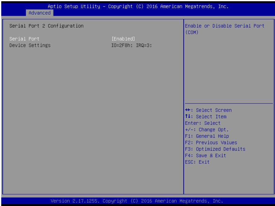
![Aptio Setup Utility - Copyright (C) 2016 American Megatrends, Inc.\nAdvanced\nSerial Port 2 Configuration\nSerial Port (Enabled)\nDevice Settings IO=2F8h; IRQ=3;\nEnable or Disable Serial Port\n(COM)\n+: Select Screen\n↑↓: Select Item\nEnter: Select\n+/-: Change Opt.\nF1: General Help\nF2: Previous Values\nF3: Optimized Defaults\nF4: Save & Exit\nESC: Exit\nVersion 2.17.1255. Copyright (C) 2016 American Megatrends, Inc.](.vpx3010-50-15107-2000-10/f2df23988a0a3a8d1088a18d8862d80b2e4f66cea95636417eb5f0c71d917f4f.jpg)

# Serial Port

Enable or Disable the Serial Port (COM).

# Device Settings

Display the serial port current resource settings.

# 8.3.3 Serial Port Console Redirection

You can use this screen to select options for the Serial Port Console Redirection settings (COM1 is unavailable for console redirection because it for IPMC use). Use the up and down &lt;Arrow&gt; keys to select an item. Use the &lt;+&gt; and &lt;-&gt; keys to change the value of the selected option. A description of the selected item appears on the right side of the screen. The settings are described on the following pages. An example of the Serial Port Console Redirection screen is shown below.
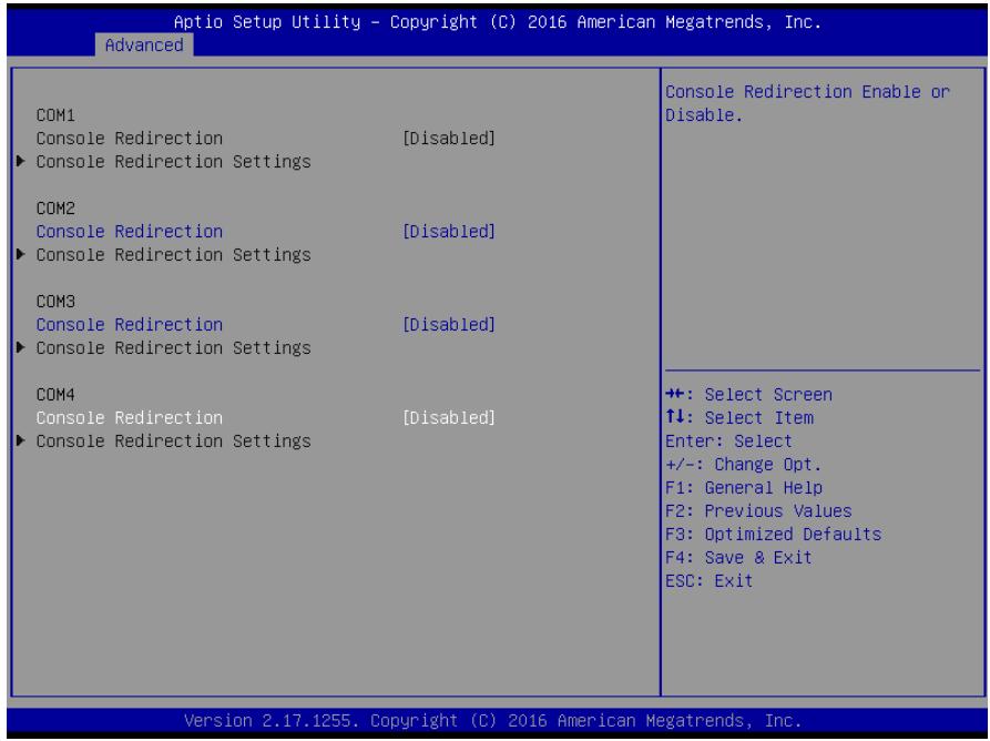
![Aptio Setup Utility - Copyright (C) 2016 American Megatrends, Inc.\nAdvanced\nCOM1\nConsole Redirection (Disabled)\n► Console Redirection Settings\nCOM2\nConsole Redirection (Disabled)\n► Console Redirection Settings\nCOM3\nConsole Redirection (Disabled)\n► Console Redirection Settings\nCOM4\nConsole Redirection (Disabled)\n► Console Redirection Settings\nConsole Redirection Enable or\nDisable.\n++: Select Screen\n↑↓: Select Item\nEnter: Select\n+/-: Change Opt.\nF1: General Help\nF2: Previous Values\nF3: Optimized Defaults\nF4: Save & Exit\nESC: Exit\nVersion 2.17.1255. Copyright (C) 2016 American Megatrends, Inc.](.vpx3010-50-15107-2000-10/2e8fcbdae3eb15409702c7151e9bb3af446fc801d9930b77e0b5a39e159fdb8b.jpg)

# Console Redirection

Enable/Disable the Console Redirection feature.

# Console Redirection Settings

These settings specify how the host computer and the remote computer exchange data. Both computers should have the same or compatible settings. The screen is shown below.

Aptio Setup Utility - Copyright (C) 2015 American Megatrends, Inc.

Advanced

COM1

Console Redirection Settings

Terminal Type

Bits per second

Data Bits

Parity

Stop Bits

Flow Control

VT-UTF8 Combo Key Support

Recorder Mode

Resolution 100x31

Legacy OS Redirection Resolution

Putty KeyPad

Redirection After BIOS POST

[ANSI]

[115200]

[8]

[None]

[1]

[None]

[Enabled]

[Disabled]

[Disabled]

[80×24]

[VT100]

[Always Enable]

Emulation: ANSI: Extended

ASCII char set. VT100: ASCII

char set. VT100+: Extends

VT100 to support color,

function keys, etc. VT-UTF8:

Uses UTF8 encoding to map

Unicode chars onto 1 or more bytes.

←: Select Screen

↑↓: Select Item

Enter: Select

+/-: Change Opt.

F1: General Help

F2: Previous Values

F3: Optimized Defaults

F4: Save & Exit

ESC: Exit

Version 2.17.1245. Copyright (C) 2015 American Megatrends, Inc.

# Terminal Type

VT100+ is the preferred terminal type for out-of-band management. Configuration options: VT100, VT100+, VT-UTF8, ANSI.

# Bits per second

Select the bits per second you want the serial port to use for console redirection. The options are 115200, 57600, 38400, 19200, 9600.

# Data Bits

Select the data bits you want the serial port to use for console redirection. Set this value to 7, 8.

# Parity

Set this option to select Parity for console redirection. The settings for this value are None, Even, Odd, Mark, Space.

# Stop Bits

Stop bits indicate the end of a serial data packet. (A start bit indicates the beginning). The standard setting is 1 stop bit. Communication with slow devices may require more than 1 stop bit. Set this value to 1 and 2.

# Flow Control

Set this option to select Flow Control for console redirection. The settings for this value are None, Hardware RTS/CTS.

# VT-UTF8 Combo Key Support

Enables VT-UTF8 combination key support for ANSI/VT100 terminals. Set this value to Enabled/Disabled.

# Recorder Mode

When this mode is enabled, only text will be sent. This is to capture terminal data. Set this value to Enabled/Disabled.

# Resolution 100x31

Set this option to extended terminal resolution. Set this value to Enabled/Disabled.

# Legacy OS Redirection

On legacy OS, the number of rows and columns supported for redirection. Set this value to 80x24, 80x25.

# Putty Key Pad

Select FunctionKey and KeyPad on Putty. Set this value to VT100, LINUX, XTERMR6, SCO, ESCN, VT400.

# Redirection After BIOS POST

The settings specify if BootLoader is selected than legacy console redirection is disabled before booting to legacy O.S. Default value is Always Enable which means legacy console redirection is enabled for legacy O.S. Set this value to Always Enable, BootLoader.

# 8.3.4 PCI Subsystem Settings

You can use this screen to select options for the PCI Subsystem Settings. Use the up and down &lt;Arrow&gt; keys to select an item. The screen is shown below.

<table><tr><td colspan="3">Aptio Setup Utility - Copyright (C) 2016 American Megatrends, Inc. Advanced</td></tr><tr><td>PCI Bus Driver Version</td><td>A5.01.08</td><td rowspan="2">Enables or Disables 64bit capable Devices to be Decoded in Above 4G Address Space(Only if System Supports 64 bit PCI Decoding).</td></tr><tr><td>PCI Devices Common Settings:Above 4G DecodingSR-IOV Support</td><td>[Disabled][Disabled]</td></tr><tr><td></td><td></td><td>++: Select Screen↑↓: Select ItemEnter: Select+/-: Change Opt.F1: General HelpF2: Previous ValuesF3: Optimized DefaultsF4: Save &amp; ExitESC: Exit</td></tr><tr><td colspan="3">Version 2.17.1255. Copyright (C) 2016 American Megatrends, Inc.</td></tr></table>

# Above 4G Decoding

Allow 64-bit capable device to be decoded above the 4G address space. Set this value to Enabled, Disabled.

# SR-IOV Support

If the system has SR-IOV capable PCIe devices, this option enables or disables Single Root IO Virtualization Support. Set this value to Enabled, Disabled.

# 8.3.5 Network Stack Configuration

You can use this screen to select options for the Network Stack Configuration.

![Aptio Setup Utility - Copyright (C) 2015 American Megatrends, Inc.\nAdvanced\nNetwork Stack	(Enabled)\nIpv4 PXE Support	(Enabled)\nIpv6 PXE Support	(Enabled)\nPXE boot wait time	0\nMedia detect count	1\nEnable/Disable UEFI Network\nStack\n+: Select Screen\n↑↓: Select Item\nEnter: Select\n+/-: Change Opt.\nF1: General Help\nF2: Previous Values\nF3: Optimized Defaults\nF4: Save & Exit\nESC: Exit\nVersion 2.17.1245. Copyright (C) 2015 American Megatrends, Inc.](.vpx3010-50-15107-2000-10/4bfc0013a444ee5fa2f56fe886f7cff4cf4ca437a02228a2e6467c1a2fd61c6c.jpg)

# Network Stack

Enable/Disable UEFI Network Stack. Set this value to Enabled, Disabled.

# IPv4 PXE Support

Enable/Disable IPv4 PXE boot support. If disabled IPv4 PXE boot option will not be created.

# IPv6 PXE Support

Enable/Disable IPv6 PXE boot support. If disabled IPv6 PXE boot option will not be created.

# PXE Boot Wait Time

Wait time to press ESC key to abort the PXE boot. Set this value to integer.

# Media Detect Count

Number of times presence of media will be checked. Set this value to integer.

# 8.3.6 CSM Configuration

You can use this screen to select options for the CSM Configuration. Use the up and down &lt;Arrow&gt; keys to select an item. Use the &lt;+&gt; and &lt;-&gt; keys to change the value of the selected option.

<table><tr><td colspan="2">Aptio Setup Utility - Copyright (C) 2016 American Megatrends, Inc. Advanced</td></tr><tr><td>Compatibility Support Module Configuration</td><td>Enable/Disable CSM Support.</td></tr><tr><td>CSM Support [Enabled]</td><td></td></tr><tr><td>CSM16 Module Version 07.79</td><td></td></tr><tr><td>Boot option filter [UEFI and Legacy]</td><td></td></tr><tr><td>Option ROM execution</td><td></td></tr><tr><td>Network [Do not launch]</td><td></td></tr><tr><td>Storage [Legacy]</td><td></td></tr><tr><td>Video [Legacy]</td><td></td></tr><tr><td></td><td>++: Select Screen↑↓: Select ItemEnter: Select+/-: Change Opt.F1: General HelpF2: Previous ValuesF3: Optimized DefaultsF4: Save &amp; ExitESC: Exit</td></tr></table>

# CSM Support

Enable/Disable CSM Support.

# Boot Option Filter

This option controls whether to hide Legacy/UEFI boot options. Set this value to UEFI and Legacy, Legacy only, UEFI only.

# Network

Controls the execution of UEFI and Legacy PXE OpROM. Set this value to Do not launch, UEFI, Legacy.

# Storage

Controls the execution of UEFI and Legacy PXE OpROM. Set this value to Do not launch, UEFI, Legacy

# Video

Controls the execution of UEFI and Legacy Video OpROM. Set this value to Do not launch, UEFI, Legacy

# 8.3.7 Hardware Monitor

You can use this screen to select options for the Hardware Monitor. Use the up and down &lt;Arrow&gt; keys to select an item. Use the &lt;+&gt; and &lt;-&gt; keys to change the value of the selected option. A description of the selected item appears on the right side of the screen. The settings are described on this page. The screen is shown below.

<table><tr><td colspan="2">Aptio Setup Utility - Copyright (C) 2016 American Megatrends, Inc. Advanced</td></tr><tr><td>PC Health Status</td><td></td></tr><tr><td>CPU temperature : +62 %</td><td></td></tr><tr><td>System temperature : +36 %</td><td></td></tr><tr><td>3.3V : +3.280 V</td><td></td></tr><tr><td>5V : +5.000 V</td><td></td></tr><tr><td>12V : +12.060 V</td><td></td></tr><tr><td></td><td>++: Select Screen
↑↓: Select Item
Enter: Select
+/-: Change Opt.
F1: General Help
F2: Previous Values
F3: Optimized Defaults
F4: Save &amp; Exit
ESC: Exit</td></tr><tr><td colspan="2">Version 2.17.1255. Copyright (C) 2016 American Megatrends, Inc.</td></tr></table>

# CPU Temperature

Display current CPU temperature.

# System Temperature

Display current system temperature.

# 3.3V

Display current system 3.3V voltage.

# 5V

Display current system 5V voltage.

# 12V

Display current system 12V voltage.

# 8.3.8 USB Configuration

You can use this screen to select options for the USB Configuration. Use the up and down &lt;Arrow&gt; keys to select an item. Use the &lt;+&gt; and &lt;-&gt; keys to change the value of the selected option. A description of the selected item appears on the right side of the screen. The screen is shown below.

<table><tr><td colspan="2">Aptio Setup Utility - Copyright (C) 2016 American Megatrends, Inc. Advanced</td></tr><tr><td>USB ConfigurationUSB Module Version 13USB Controllers:1 EHCI, 1 XHCIUSB Devices:1 Drive, 1 Keyboard, 2 HubsLegacy USB Support [Enabled]XHCI Hand-off [Enabled]EHCI Hand-off [Disabled]USB Mass Storage Driver Support [Enabled]Port 60/64 Emulation [Enabled]Mass Storage Devices:JetFlashTranscend 32GB 1100 [Auto]</td><td>Enables Legacy USB support.AUTO option disables legacysupport if no USB devices areconnected.DISABLE option willkeep USB devices availableonly for EFI applications.++: Select Screen↑↓: Select ItemEnter: Select+/-: Change Opt.F1: General HelpF2: Previous ValuesF3: Optimized DefaultsF4: Save &amp; ExitESC: Exit</td></tr><tr><td colspan="2">Version 2.17.1255. Copyright (C) 2016 American Megatrends, Inc.</td></tr></table>

# Legacy USB Support

Enables Legacy USB Support. Auto option disables legacy support if no USB devices are connected. Disable option will keep USB devices available only for EFI applications.

# XHCI Hand-off

This is a workaround for OSes without XHCI hand-off support. The XHCI ownership change should be claimed by XHCI driver.

# EHCI Hand-off

This is a workaround for OSes without EHCl hand-off support. The EHCl ownership change should be claimed by EHCl driver.

# USB Mass Storage Driver Support

Enable/Disable USB mass storage driver support.

# Port 60/64 Emulation

Enable I/O port 60h/64h emulation support. This should be enabled for complete USB keyboard legacy support for non-USB aware OSes.

# 8.4 IntelRCSetup

Select the IntelRCSetup tab from the setup screen to enter the IntelRCSetup screen. You can select any of IntelRCSetup options by highlighting it using the &lt;Arrow&gt; keys. The IntelRCSetup screen is shown below.

<table><tr><td colspan="2">Aptio Setup Utility - Copyright (C) 2016 American Megatrends, Inc.Main Advanced IntelRCSetup Security Boot Event Logs Save &amp; Exit</td></tr><tr><td rowspan="27">CPU ConfigurationAdvanced Power Management ConfigurationMemory ConfigurationIIO ConfigurationPCH Configuration----Setup Warning:Setting items on this Screen to incorrect values may cause system to malfunction!</td><td rowspan="26">Displays and provides option to change the CPU Settings++: Select Screen↑↓: Select ItemEnter: Select+/-: Change Opt.F1: General HelpF2: Previous ValuesF3: Optimized DefaultsF4: Save &amp; ExitESC: Exit</td></tr><tr></tr><tr></tr><tr></tr><tr></tr><tr></tr><tr></tr><tr></tr><tr></tr><tr></tr><tr></tr><tr></tr><tr></tr><tr></tr><tr></tr><tr></tr><tr></tr><tr></tr><tr></tr><tr></tr><tr></tr><tr></tr><tr></tr><tr></tr><tr></tr><tr></tr><tr><td></td></tr></table>

# 8.4.1 CPU Configuration

You can use this screen to select options for the CPU Configuration. Use the up and down &lt;Arrow&gt; keys to select an item. Use the &lt;+&gt; and &lt;-&gt; keys to change the value of the selected option. A description of the selected item appears on the right side of the screen. The screen is shown below.

<table><tr><td colspan="2">CPU Configuration</td><td rowspan="13">Number of Cores to Enable. 0 means all cores. 2 Cores available.</td></tr><tr><td>Processor ID</td><td>00050663</td></tr><tr><td>Processor Cores</td><td>2</td></tr><tr><td>Processor Stepping</td><td>V2/V3</td></tr><tr><td>Processor Frequency</td><td>1.200GHz</td></tr><tr><td>Processor Max Ratio</td><td>0CH</td></tr><tr><td>Processor Min Ratio</td><td>08H</td></tr><tr><td>Microcode Revision</td><td>07000005</td></tr><tr><td>L1 Cache RAM</td><td>128KB</td></tr><tr><td>L2 Cache RAM</td><td>512KB</td></tr><tr><td>L3 Cache RAM</td><td>3072KB</td></tr><tr><td>Processor 0 Version</td><td>Intel(R) Pentium(R) CPU D1507 @ 1.20GHz</td></tr><tr><td></td><td></td></tr><tr><td>Cores Enabled</td><td>0</td><td rowspan="9">+: Select Screen
↑↓: Select Item
Enter: Select
+/-: Change Opt.
F1: General Help
F2: Previous Values
F3: Optimized Defaults
F4: Save &amp; Exit
ESC: Exit</td></tr><tr><td>Hyper-Threading [ALL]</td><td>[Enable]</td></tr><tr><td>Execute Disable Bit</td><td>[Enable]</td></tr><tr><td>Enable Intel TXT Support</td><td>[Disable]</td></tr><tr><td>VMX</td><td>[Enable]</td></tr><tr><td>Enable SMX</td><td>[Disable]</td></tr><tr><td>Lock Chipset</td><td>[Enable]</td></tr><tr><td>MSR Lock Control</td><td>[Enable]</td></tr><tr><td>Hardware Prefetcher</td><td>[Enable]</td></tr></table>

# Cores Enabled

Number of CPU cores to be enabled. 0 means all cores.

# Hyper-Threading [ALL]

Enables Hyper Threading (Software Method to Enable/Disable Logical Processor threads). Set this value to Enabled, Disabled.

# Enable Intel TXT Support

Enables Intel Trusted Execution Technology Configuration. Set this value to Enabled, Disabled.

# VMX

Enables the Vanderpool Technology, takes effect after reboot. Set this value to Enabled, Disabled.

# Enable SMX

Enables safer mode extensions. Set this value to Enabled, Disabled.

# Lock Chipset

Lock or unlock chipset. Set this value to Enabled, Disabled.

# MSR Lock Control

MSR 2Ah, MSR 0E2h and CSR 80h will be lock when enabled. Set this value to Enabled, Disabled.

# Hardware Prefetcher

MLC streamer pre-fetcher. Set this value to Enabled, Disabled.

# Adjacent Cache Prefetcher

MLC spatial pre-fetcher. Set this value to Enabled, Disabled.

# X2APIC

Enable or disable extended APIC support. Set this value to Enabled, Disabled.

# 8.4.2 Advanced Power Management Configuration

You can use this screen to select options for the Advanced Power Management Configuration. Use the up and down &lt;Arrow&gt; keys to select an item. Use the &lt;+&gt; and &lt;-&gt; keys to change the value of the selected option. A description of the selected item appears on the right side of the screen. The screen is shown below.

<table><tr><td rowspan="2">Advanced Power Management Configuration
EIST (P-states) [Enable]
Config TDP [Disable]
►CPU P State Control
►CPU C State Control
►CPU T State Control</td><td>When enabled, OS sets CPU frequency according load. When disabled, CPU frequency is set at max non-turbo.</td></tr><tr><td>+: Select Screen
↑↓: Select Item
Enter: Select
+/-: Change Opt.
F1: General Help
F2: Previous Values
F3: Optimized Defaults
F4: Save &amp; Exit
ESC: Exit</td></tr><tr><td colspan="2">Version 2.17.1255. Copyright (C) 2016 American Megatrends, Inc.</td></tr></table>

# EIST (P-states)

When enabled, OS sets CPU frequency according load. When disabled, CPU frequency is set at max non-turbo. Set this value to Enable/Disable.

# Config TDP

Option to disable/enable Config TDP. Set this value to Enable/Disable.

# CPU P State Control

The screen is shown below

<table><tr><td colspan="2">CPU P State Control</td><td rowspan="6">Per Logical: indicates the P-state domain for each logical proc in the system. Per Package: all procs indicate the same domain in the same package.</td></tr><tr><td>P State Domain</td><td>[ALL]</td></tr><tr><td>P-state coordination</td><td>[HW_ALL]</td></tr><tr><td>Energy efficient P-state</td><td>[Enable]</td></tr><tr><td>Boot performance mode</td><td>[Max Performance]</td></tr><tr><td>Turbo Mode</td><td>[Enable]</td></tr><tr><td></td><td></td><td>+: Select Screen↑↓: Select ItemEnter: Select+/-: Change Opt.F1: General HelpF2: Previous ValuesF3: Optimized DefaultsF4: Save &amp; ExitESC: Exit</td></tr><tr><td colspan="3">Version 2.17.1255. Copyright (C) 2016 American Megatrends, Inc.</td></tr></table>

# P State Domain

Select the P-state domain for each logical processor in system by logical. When by package all processor indicate the same domain in the same package. Set this value to ALL, ONE.

# P-State Coordination

Select P-state coordination. HW\_ALL coordination is recommended over SW\_ALL and SW\_ANY. Set this value to HW\_ALL, SW\_ALL, SW\_ANY.

# Energy Efficient P-state

Select the Energy Efficient P-state feature. Set this value to Enable/Disable.

# Boot Performance Mode

Select the performance state that BIOS will set before handoff to OS. Set this value to Max Performance, Max Efficient.

# Turbo Mode

Select CPU Turbo mode. Set this value to Enable/Disable.

# CPU C State Control

The screen is shown below

<table><tr><td>CPU C State Control
C2C3TT
CPU C State
Package C State limit
CPU C3 report
CPU C6 report
Enhanced Halt State (C1E)
OS ACPI Cx</td><td>0
[Enable]
[C6(Retention) state]
[Disable]
[Enable]
[Enable]
[ACPI C2]</td><td>Default = 0, means [AUTO].
C2 to C3 Transition Timer,
PPDN_INIT = 1:10:1:74
Bit[11:0].</td></tr><tr><td></td><td></td><td>+: Select Screen
↑↓: Select Item
Enter: Select
+/-: Change Opt.
F1: General Help
F2: Previous Values
F3: Optimized Defaults
F4: Save &amp; Exit
ESC: Exit</td></tr><tr><td colspan="3">Version 2.17.1255, Copyright (C) 2016 American Megatrends, Inc.</td></tr></table>

# C2C3TT

Select C2 to C3 transition timer. Default 0 means Auto.

# CPU C State

Select CPU Enhanced Cx state. Set this value to Enable/Disable.

# Package C State Limit

Select CP package C state limit. Set this value to C0, C1state, C2state, C6(non Retention) state, C6(Retention) state, No Limit.

# CPU C3 Report

Select CPU C3(APCI C2) report to OS recommended to be disabled. Set this value to Enable/Disable.

# CPU C6 Report

Select CPU C6(APCI C2) report to OS recommended to be enabled. Set this value to Enable/Disable.

# Enhance Halt State (C1E)

Select the CPU enhanced C1E state. It takes effect after reboot. Set this value to Enable/Disable.

# OS APCI Cx

Select the CC3/CC6 report to OS ACPI C2 or ACPI C3. Set this value to ACPI C2, APCI C3.

# CPU T State Control

The screen is shown below

<table><tr><td rowspan="2">CPU T State Control
ACPI T-States [Disable]</td><td>Enable/Disable CPU throttling by OS. Throttling reduces power consumption.</td></tr><tr><td>+: Select Screen
↑↓: Select Item
Enter: Select
+/-: Change Opt.
F1: General Help
F2: Previous Values
F3: Optimized Defaults
F4: Save &amp; Exit
ESC: Exit</td></tr><tr><td colspan="2">Version 2.17.1255, Copyright (C) 2016 American Megatrends, Inc.</td></tr></table>

# ACPI T-States

Enable/Disable CPU throttling by OS. Throttling reduces power consumption. Set this value to Enable/Disable.

# 8.4.3 Memory Configuration

This screen displays the Memory Configuration of the system.

<table><tr><td colspan="2">-Aptio Setup Utility - Copyright (C) 2016 American Megatrends, Inc.
IntelRCSetup</td></tr><tr><td rowspan="2">-------- Integrated Memory Controller (iMC)
-------- Socket0.Ch0.Dimm0: 1600MT/s Micron SRx8 8GB SODIMM
Socket0.Ch1.Dimm0: 1600MT/s Micron SRx8 8GB SODIMM</td><td></td></tr><tr><td>+: Select Screen
↑↓: Select Item
Enter: Select
+/-: Change Opt.
F1: General Help
F2: Previous Values
F3: Optimized Defaults
F4: Save &amp; Exit
ESC: Exit</td></tr><tr><td colspan="2">Version 2.17.1255. Copyright (C) 2016 American Megatrends, Inc.</td></tr></table>

# 8.4.4 IIO Configuration

You can use this screen to select options for the IIO Configuration. Use the up and down &lt;Arrow&gt; keys to select an item. Use the &lt;+&gt; and &lt;-&gt; keys to change the value of the selected option. A description of the selected item appears on the right side of the screen. The screen is shown below.

<table><tr><td colspan="2">Aptio Setup Utility - Copyright (C) 2016 American Megatrends, Inc.
IntelRCSetup</td></tr><tr><td rowspan="2">IIO Configuration
► IIOO Configuration
► IIO General Configuration
► Intel VT for Directed I/O (VT-d)</td><td></td></tr><tr><td>+: Select Screen
↑↓: Select Item
Enter: Select
+/-: Change Opt.
F1: General Help
F2: Previous Values
F3: Optimized Defaults
F4: Save &amp; Exit
ESC: Exit</td></tr><tr><td colspan="2">Version 2.17.1255. Copyright (C) 2016 American Megatrends, Inc.</td></tr></table>

# IIO0 Configuration

The screen is shown below

<table><tr><td colspan="2">Aptio Setup Utility - Copyright (C) 2016 American Megatrends, Inc.</td></tr><tr><td colspan="2">IntelRCSetup</td></tr><tr><td rowspan="2">IOU2 (IIO PCIe Port 1) [Auto]IOU0 (IIO PCIe Port 2) [Auto]IOU1 (IIO PCIe Port 3) [x16]Socket 0 PcieD01F0 - Port 1ASocket 0 PcieD02F0 - Port 2ASocket 0 PcieD02F2 - Port 2CSocket 0 PcieD03F0 - Port 3A</td><td>Selects PCIe port Bifurcation for selected slot(s)</td></tr><tr><td>++: Select Screen↑↓: Select ItemEnter: Select+/-: Change Opt.F1: General HelpF2: Previous ValuesF3: Optimized DefaultsF4: Save &amp; ExitESC: Exit</td></tr><tr><td colspan="2">Version 2.17.1255. Copyright (C) 2016 American Megatrends, Inc.</td></tr></table>

# IOU2 (IIO PCIe Port 1)

Selects PCIe port Bifurcation for selected slot(s). Set this value to Auto, x8, x4x4.

# IOU0 (IIO PCIe Port 2)

Selects PCIe port Bifurcation for selected slot(s). Set this value to Auto, x16, x8x8, x8x4x4, x4x4x8, x4x4x4x4.

# IOU1 (IIO PCIe Port 3)

Selects PCIe port Bifurcation for selected slot(s). Set this value to Auto, x16, x8x8, x8x4x4, x4x4x8, x4x4x4x4. (PS: If XMC SKU default is x8x8, PCIE SKU default is x16)

# IIO General Configuration

The screen is shown below

<table><tr><td colspan="2">Aptio Setup Utility - Copyright (C) 2016 American Megatrends, Inc. IntelRCSetup</td></tr><tr><td rowspan="2">TXT DPR memory setting [3M DPR] IIO 0 IIO IOAPIC [Enable]</td><td>Allows selection of the TXT DPR size in system</td></tr><tr><td>++: Select Screen ↑↓: Select Item Enter: Select +/-: Change Opt. F1: General Help F2: Previous Values F3: Optimized Defaults F4: Save &amp; Exit ESC: Exit</td></tr></table>

# TXT DPR Memory Setting

Select TXT DPR size in system. Set this value to 1M DPR, 3M DPR, 64M DPR, 128M DPR, 255M DPR.

# IIO IOAPIC

Enable or disable IIO IOAPIC. Set this value to Enabled/Disabled.

# Intel VT for Directed I/O (VT-d)

The screen is shown below

<table><tr><td colspan="2">Aptio Setup Utility - Copyright (C) 2016 American Megatrends, Inc.</td></tr><tr><td rowspan="2">Intel VT for Directed I/O (VT-d) ----Intel VT for Directed I/O (VT-d) [Enable]</td><td>Enable/Disable Intel Virtualization Technology for Directed I/O (VT-d) by reporting the I/O device assignment to VMM through DMAR ACPI Tables.</td></tr><tr><td>++: Select Screen↑↓: Select ItemEnter: Select+/-: Change Opt.F1: General HelpF2: Previous ValuesF3: Optimized DefaultsF4: Save &amp; ExitESC: Exit</td></tr></table>

Enable or disable Intel Virtualization Technology for directed I/O(VT-d) by reporting the I/O device assignment to VMM through DMAR ACPI tables. Set this value to Enabled/Disabled.

# 8.4.5 PCH Configuration

You can use this screen to select options for the PCH Configuration. Use the up and down &lt;Arrow&gt; keys to select an item. Use the &lt;+&gt; and &lt;-&gt; keys to change the value of the selected option. A description of the selected item appears on the right side of the screen. The screen is shown below.

<table><tr><td colspan="2">Aptio Setup Utility - Copyright (C) 2016 American Megatrends, Inc.
IntelRCSetup</td></tr><tr><td rowspan="2">PCH Configuration
PCH state after G3 [S0]
► PCH SATA Configuration
► USB Configuration</td><td>Select S0/S5 for ACPI state after a G3</td></tr><tr><td>+: Select Screen
↑↓: Select Item
Enter: Select
+/-: Change Opt.
F1: General Help
F2: Previous Values
F3: Optimized Defaults
F4: Save &amp; Exit
ESC: Exit</td></tr><tr><td colspan="2">Version 2.17.1255. Copyright (C) 2016 American Megatrends, Inc.</td></tr></table>

# PCH State After G3

Select S0/S5 for ACPI state after system return from G3. Set this value to S0, S5.

# PCH SATA Configuration

The screen is shown below

Aptio Setup Utility - Copyright (C) 2016 American Megatrends, Inc.
IntelRCSetup

<table><tr><td colspan="2">PCH SATA Configuration----</td><td rowspan="13">Enable or Disable SATAController</td></tr><tr><td>SATA Controller</td><td>[Enabled]</td></tr><tr><td>Configure SATA as</td><td>[AHCI]</td></tr><tr><td>SATA Controller Speed</td><td>[Default]</td></tr><tr><td>SATA Port 0</td><td>[Not Installed]</td></tr><tr><td>Port 0</td><td>[Enabled]</td></tr><tr><td>SATA Device Type</td><td>[Hard Disk Drive]</td></tr><tr><td>SATA Port 1</td><td>ASD26-HA2032-E - 31.6...</td></tr><tr><td>Port 1</td><td>[Enabled]</td></tr><tr><td>SATA Device Type</td><td>[Hard Disk Drive]</td></tr><tr><td>SATA Port 2</td><td>[Not Installed]</td></tr><tr><td>Port 2</td><td>[Enabled]</td></tr><tr><td>SATA Device Type</td><td>[Hard Disk Drive]</td></tr><tr><td></td><td></td><td>+: Select Screen↑↓: Select ItemEnter: Select+/-: Change Opt.F1: General HelpF2: Previous ValuesF3: Optimized DefaultsF4: Save &amp; ExitESC: Exit</td></tr></table>

Version 2.17.1255. Copyright (C) 2016 American Megatrends, Inc.

# SATA Controller

Enable or disable SATA controller. Set this value to Enabled/Disabled.

# Configure SATA as

This will configure SATA as IDE, RAID or AHCI. Set this value to IDE, AHCI, RAID.

# SATA Controller Speed

Select SATA controller speed. Set this value to Default, Gen1, Gen2, Gen3.

# SATA Port 0-2

Allow enable or disable SATA ports. Set this value to Enabled/Disabled.

# SATA Device Type

Select SATA devices' type. Set this value to Hard Disk Drive, Solid State Drive.

![The image displays a white document icon with a black outline and a folded top-right corner. Horizontal black lines are visible near the bottom of the document. A large, bold red checkmark is superimposed over the center of the document.](.vpx3010-50-15107-2000-10/5b7d038960ed544b93ed251390f273aa742e91a1ff7a26bbe1b893c2f1030586.jpg)
NOTE:

"SATA Port 2" only on PCIe SKU.

# USB Configuration

The screen is shown below

<table><tr><td colspan="2">Aptio Setup Utility - Copyright (C) 2016 American Megatrends, Inc.
IntelRCSetup</td></tr><tr><td>xHCI Mode [Auto]
USB Ports Per-Port Disable Control [Disabled]</td><td>Mode of operation of xHCI controller.</td></tr></table>

# xHCI Mode

Select xHCI controller operation modes. Set this value to Smart Auto, Auto, Enabled, Disabled.

# USB Per-Port Disable Control

Allow control disable and enable of the USB ports. Set this value to Enabled/Disabled.

# 8.5 Security Setup

<table><tr><td colspan="2">Aptio Setup Utility - Copyright (C) 2016 American Megatrends, Inc.Main Advanced IntelRCSetup Security Boot Event Logs Save &amp; Exit</td></tr><tr><td>Password DescriptionIf ONLY the Administrator&#x27;s password is set,then this only limits access to Setup and isonly asked for when entering Setup.If ONLY the User&#x27;s password is set, then thisis a power on password and must be entered toboot or enter Setup. In Setup the User willhave Administrator rights.The password length must bein the following range:Minimum length 3Maximum length 20Administrator PasswordUser Password▶ Secure Boot menu</td><td>Set Administrator Password++: Select Screen↑↓: Select ItemEnter: Select+/-: Change Opt.F1: General HelpF2: Previous ValuesF3: Optimized DefaultsF4: Save &amp; ExitESC: Exit</td></tr></table>

# Administrator, User Password

If only the administrator's password is set, then this only limits access to setup and is only asked for when entering setup.

If only the user's password is set, then this is a power on password and must be entered to boot or enter setup. In setup the user will have administrator rights.

# Secure Boot Menu

Customization of Secure Boot settings.

# 8.6 Boot Settings

Select the Boot tab from the setup screen to enter the Boot BIOS Setup screen. You can select any of the items in the left frame of the screen, such as Boot Device Priority, to go to the sub menu for that item. You can display a Boot BIOS Setup option by highlighting it using the &lt;Arrow&gt; keys. The Boot Settings screen is shown below:

<table><tr><td colspan="2">Aptio Setup Utility - Copyright (C) 2016 American Megatrends, Inc.
Main Advanced IntelRCSetup Security Boot Event Logs Save &amp; Exit</td></tr><tr><td rowspan="2">Boot Configuration
Setup Prompt Timeout
Bootup NumLock State
Quiet Boot
Boot Option Priorities
Boot Option #1
Boot Option #2
Boot Option #3
New Boot Option Policy
Hard Drive BBS Priorities</td><td>Number of seconds to wait for setup activation key.
65535(0xFFFF) means indefinite waiting.</td></tr><tr><td>+: Select Screen
↑↓: Select Item
Enter: Select
+/-: Change Opt.
F1: General Help
F2: Previous Values
F3: Optimized Defaults
F4: Save &amp; Exit
ESC: Exit</td></tr><tr><td colspan="2">Version 2.17.1255. Copyright (C) 2016 American Megatrends, Inc.</td></tr></table>

# Setup Prompt Timeout

Set number of seconds that system waiting for setup activation key. The number of 65535 (0xFFFF) means indefinite waiting.

# Bootup NumLock State

Select the keyboard NumLock state. Set this value to On, Off.

# Quiet Boot

▶ Disabled - Set this value to allow the computer system to display the POST messages.
▶ Enabled - Set this value to allow the computer system to display the OEM logo.

# Set Boot Priority

Set Boot Option #1 \~2 boot priority.

# New Boot Option Policy

Select the placement of newly detected UEFI boot options. Set this value to Default, Place First, Place Last.

# Hard Drive BBS Priorities

Specifies the boot device priority sequence from available hard drives.

# 8.7 Save & Exit Menu

Select the Save & Exit tab from the setup screen to enter the Save & Exit BIOS Setup screen. You can display an Exit BIOS Setup option by highlighting it using the &lt;Arrow&gt; keys. The Save & Exit BIOS Setup screen is shown below.

<table><tr><td colspan="2">Aptio Setup Utility - Copyright (C) 2016 American Megatrends, Inc.Main Advanced IntelRCSetup Security Boot Event Logs Save &amp; Exit</td></tr><tr><td>Save OptionsSave Changes and ExitDiscard Changes and ExitSave Changes and ResetDiscard Changes and ResetSave ChangesDiscard ChangesDefault OptionsRestore DefaultsSave as User DefaultsRestore User DefaultsBoot OverrideP1: ASD26-HA2032-ETUEFI: SanDisk, Partition 1UEFI: Built-in EFI Shell</td><td>Exit system setup after saving the changes.++: Select Screen↑↓: Select ItemEnter: Select+/-: Change Opt.F1: General HelpF2: Previous ValuesF3: Optimized DefaultsF4: Save &amp; ExitESC: Exit</td></tr><tr><td colspan="2">Version 2.17.1255. Copyright (C) 2016 American Megatrends, Inc.</td></tr></table>

# Save Changes and Exit

Exit the system after saving the changes.

![Save & Exit Setup\nSave configuration and exit?\nYes	No](.vpx3010-50-15107-2000-10/aa03fb9e255134e0419f52c2db0371b90cb4a3911cba1c5333bb3305cd32a617.jpg)

# Discard Changes and Exit

Exit system setup without saving any changes.

![Exit Without Saving\nQuit without saving?\nYes No](.vpx3010-50-15107-2000-10/1e41f446bfec6fc5da7a3af06837c2cb7a1932c66b2fdd53d63c93af7d83aedc.jpg)

# Save Changes and Reset

Reset the system after saving the changes.

![---- Save & reset ----\n| Save configuration and reset?\n----\nYes No](.vpx3010-50-15107-2000-10/1604248a92fcd00323bdcc0fd3d75fc01b56190bd40c4cba9a05182e8078b28f.jpg)

# Discard Changes and Reset

Reset system setup without saving any changes.

![- Reset Without Saving\nReset without saving?\n----\nYes No](.vpx3010-50-15107-2000-10/7f5e98b66a4e266a835355da1555ff1c5c5a85059c8753728e2cdf3a91a68af4.jpg)

# Save Changes

Save changes done so far to any of the setup options.

![- Save Setup Values -\nSave configuration?\n----\nYes No](.vpx3010-50-15107-2000-10/27df9849b37820217feedc7b499a8098c29c537917bcd069779c9af02f56f2ae.jpg)

# Discard Changes

Discard changes done so far to any of the setup options.

![- Load Previous Values\nLoad Previous Values?\n-\nYes No](.vpx3010-50-15107-2000-10/d5cf3e6c5444d2184e4c3e65468a84913d1468b1bc8b2ebe3caff2573a32c92a.jpg)

# Restore Changes

Restore/Load Defaults values for all the setup options.

![Load Optimized Defaults -\nLoad Optimized Defaults?\nYes No](.vpx3010-50-15107-2000-10/9a2ada8bfb3fbd925a38a3277aa16ee99937a8cd0779bf8119fe86887e68a59a.jpg)

# Save as User Defaults

Save the changes done so far as user defaults..

![Save Values as User Defaults\nSave configuration?\nYes	No](.vpx3010-50-15107-2000-10/614570a11fed8ef4cbf69b35b5135b3f1715b4014132daa3017f57f326e8b2a3.jpg)

# Restore User Defaults

Save changes done so far to any of the setup options.

![Restore User Defaults -\nRestore User Defaults?\n----\nYes No](.vpx3010-50-15107-2000-10/3a2c346bea07533ec5231180ab5a050911bda6ef799a2bbb6041037b16d12ce1.jpg)

This page intentionally left blank.

# Important Safety Instructions

For user safety, please read and follow all instructions, WARNINGS, CAUTIONS, and NOTES marked in this manual and on the associated equipment before handling/operating the equipment.

▶ Read these safety instructions carefully.
- Keep this user’s manual for future reference.
▶ Read the specifications section of this manual for detailed information on the operating environment of this equipment.
▶ When installing/mounting or uninstalling/removing equipment:

▷ Turn off power and unplug any power cords/cables.

▶ To avoid electrical shock and/or damage to equipment:

▷ Keep equipment away from water or liquid sources;
▷ Keep equipment away from high heat or high humidity;
▷ Keep equipment properly ventilated (do not block or cover ventilation openings);

▶ Make sure to use recommended voltage and power source settings;

▶ Always install and operate equipment near an easily accessible electrical socket-outlet;

▷ Secure the power cord (do not place any object on/over the power cord);

▶ Only install/attach and operate equipment on stable surfaces and/or recommended mountings; and,

▷ If the equipment will not be used for long periods of time, turn off and unplug the equipment from its power source.

▶ Never attempt to fix the equipment. Equipment should only be serviced by qualified personnel.

A Lithium-type battery may be provided for uninterrupted, backup or emergency power.

![The image displays a red triangular warning sign containing a white exclamation point in the center. Directly below the triangle is the word 'WARNING:' written in black capital letters.](.vpx3010-50-15107-2000-10/48b14e765b1eb5cb1501dbb4fc87ee0d09d5e92f3dbc08b5b38f2ad527c0d772.jpg)

Risk of explosion if battery is replaced with one of an incorrect type. Dispose of used batteries appropriately.

▶ Equipment must be serviced by authorized technicians when:

▷ The power cord or plug is damaged;
▷ Liquid has penetrated the equipment;
▷ It has been exposed to high humidity/moisture;
$\triangleright$ It is not functioning or does not function according to the user's manual;
▷ It has been dropped and/or damaged; and/or,
▷ It has an obvious sign of breakage.

# Getting Service

Ask an Expert: http://askanexpert.adlinktech.com

# ADLINK Technology, Inc.

9F, No.166 Jian Yi Road, Zhonghe District

New Taipei City 235, Taiwan

Tel: +886-2-8226-5877

Fax: +886-2-8226-5717

Email: service@adlinktech.com

# Ampro ADLINK Technology, Inc.

5215 Hellyer Avenue, #110

San Jose, CA 95138, USA

Tel: +1-408-360-0200

Toll Free: +1-800-966-5200 (USA only)

Fax: +1-408-360-0222

Email: info@adlinktech.com

# ADLINK Technology (China) Co., Ltd.

300 Fang Chun Rd., Zhangjiang Hi-Tech Park

Pudong New Area, Shanghai, 201203 China

Tel: +86-21-5132-8988

Fax: +86-21-5132-3588

Email: market@adlinktech.com

# ADLINK Technology GmbH

Hans-Thoma-Strasse 11

D-68163 Mannheim, Germany

Tel: +49-621-43214-0

Fax: +49-621 43214-30

Email: emea@adlinktech.com

Please visit the Contact page at www.adlinktech.com for information on how to contact the ADLINK regional office nearest you.
[🔗 Link to the original document](.vpx3010-50-15107-2000-10/vpx3010-50-15107-2000-10.pdf)
